Introduction to VMM Feng Li State Key Laboratory

Introduction to VMM Feng Li State Key Laboratory of Particle Detection and Electronics Depart of Modern Physics, University of Science & Technology of China Acknowledgment Gianluigi De Geronimo DG Circuits Consulting, Stony Brook University, University of Michigan Shanghai, CHEP 2018

VMM ASIC family VMM: ASIC family for ATLAS Muon Spectrometer upgrade (Micromegas and Thin Gap Chamber) • VMM 1 • VMM 2 • VMM 3 VMM 1 AR 2

VMM 1 An ASIC for Micropattern Detectors

Architecture of VMM 1 neighbor logic CA shaper peak time addr 64 channels or direct timing (To. T or Tt. P) real time address (ART) mux amplitude mux timing mux address logic • dual polarity, adj. gain (0. 5, 1, 3, 9 m. V/f. C) (0. 11 to 2 p. C), adj. peaktime (25 -200 ns) • discriminator with sub-hysteresis and neighboring (channel and chip) • address of first event in real time at dedicated output (ART) • direct timing outputs: time-over-threshold or time-to-peak • peak detector, time detector <1 ns • multiplexing with sparse readout and smart token passing (channel and chip) • threshold and pulse generators, analog monitors, channel mask, temperature sensor, 600 m. V BGR, 600 m. V LVDS • power 4. 5 m. W/ch, size 6 x 8. 4 mm², process IBM CMOS 130 nm 1. 2 V CA 4

Architecture of VMM 2

Packaging of VMM 2 custom BGA package 21 x 21 mm², 400 -pin, 1 mm pitch

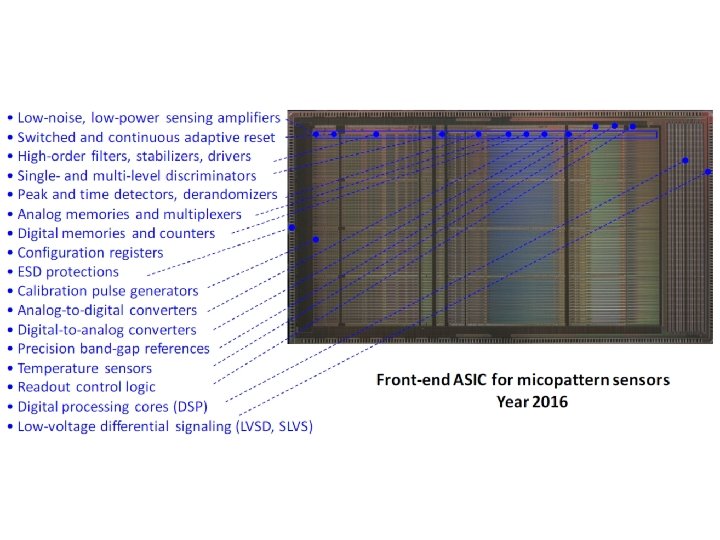
Architecture of VMM 3

Packaging of VMM 3
 VMM 3 VDDP bias RP 2 PAD VDDP CP bias RP")
Attenuation Networks (π-Networks) VMM 3 VDDP bias RP 2 PAD VDDP CP bias RP 1 VMM 3 attenuation CP/(CP+CPAD) VDDP RS 2 VDDP CS RS 1 VMM 3 STRIP VMM 3 (ac-coupled) (& termination) G. De Geronimo RS 1 300 kΩ, RS 2 300 kΩ CS > 100 p. F 10 V Small attenuation, or none Beware of inter-strip coupling No attenuation → only RS 1=100 k Cw WIRES grounding RP 1 300 kΩ, RP 2 300 kΩ CP CPAD/2 or 100 p. F 10 V Attenuation 1/3, can be adjusted No attenuation → only RP 1=100 k CWG RW 2 RW 1 1 MΩ, RW 2 300 kΩ CWG 1 n. F 10 V, CW 200 p. F 10 V Attenuation 1/6, can be adjusted CWG keeps wire impedance low Controlled termination possible No attenuation → only RW 1=300 k 10

Problem on VMM 3 • Higher gain, higher baseline • Oscillation observed, probably caused by the π -Networks of FEB channels and the POWER Vddad of VMM 3.

Thanks!

Path Towards VMM 1 VMM 2 2011 -12 50 mm² 500 k FETs (8 k/ch. ) 2013 -14 115 mm² 5 M FETs (80 k/ch. ) • mixed-signal • 2 -phase readout • peak and timing • neighboring • sub-hysteresis • few timing outputs • mixed signal • continuous fully-digital readout • current-output peak detector • increased range of gains • three ADCs per channel • FIFOs, serialized data with DDR • serialized ART with DDR • additional timing modes • 64 timing outputs • ITAR • additional functions and fixes VMM 3 2015 -16 130 mm² 10 M FETs (160 k/ch. ) • mixed signal + digital • continuous simultaneous readout • SEU-tolerant logic • deeply revised front-end for TGC (2 n. F, 50 p. C, fast recovery, . . . ) • L 0 handling digital core • SLVS and new config. interface • new reset control and fast reset • timing at threshold • timing ramp optimization • pulser range extension • ART synchronization • 32 -channel skip • additional functions and fixes 13
- Slides: 13