Introduction to VGA TA Author Trumen DE 2115UsermanualDE




![Pin Assignments Signal Name FPGA Pin No. Description VGA_R[0]~[7] PIN_E 12~H 10 VGA Red[0]~[7] Pin Assignments Signal Name FPGA Pin No. Description VGA_R[0]~[7] PIN_E 12~H 10 VGA Red[0]~[7]](https://slidetodoc.com/presentation_image/1d0176ee4e1da90ca82ffc5e8c74d1b4/image-12.jpg)


- Slides: 14

Introduction to VGA 數位電路實驗 TA: � 柏辰 Author: Trumen

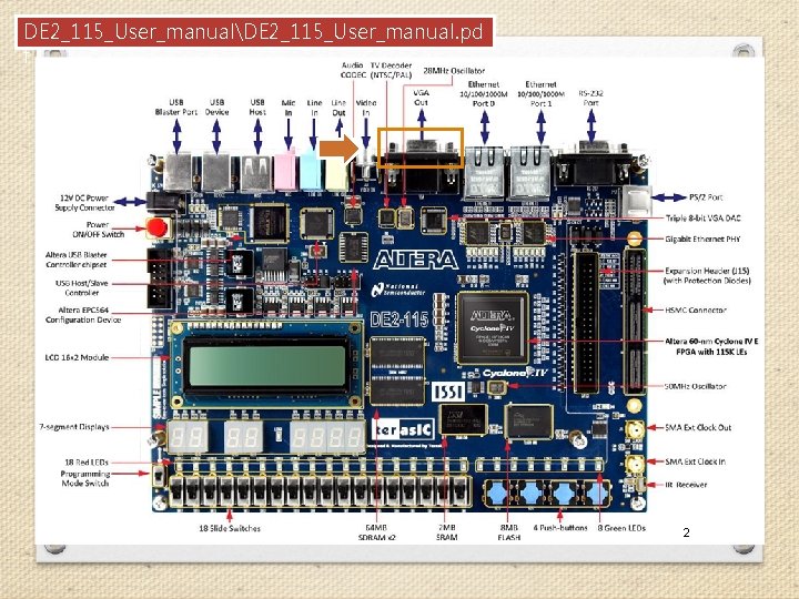
DE 2_115_User_manualDE 2_115_User_manual. pd f 2

Introduction • The DE 2 -115 board includes a 15 -pin D-SUB connector for VGA (Video Graphics Array) output. • The VGA synchronization signals are provided directly from the Cyclone IV E FPGA • The Analog Devices ADV 7123 triple 10 -bit high-speed video DAC (only the higher 8 -bit are used) is used to produce the analog data signals (red, green, and blue). 3

Introduction 4

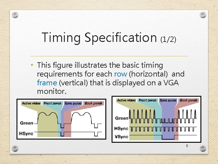
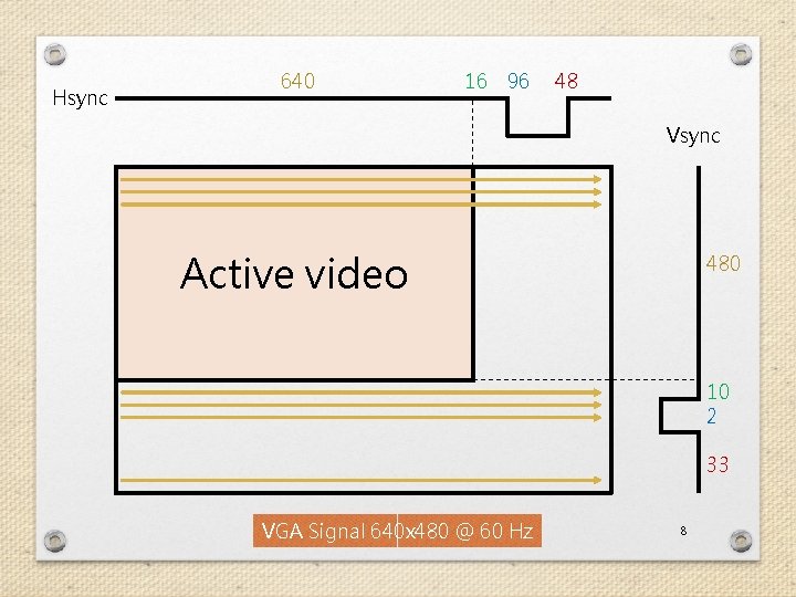
Timing Specification (1/2) • This figure illustrates the basic timing requirements for each row (horizontal) and frame (vertical) that is displayed on a VGA monitor. 5

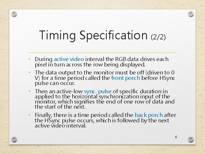
Timing Specification (2/2) • During active video interval the RGB data drives each pixel in turn across the row being displayed. • The data output to the monitor must be off (driven to 0 V) for a time period called the front porch before HSync pulse can occur. • Then an active-low sync. pulse of specific duration in applied to the horizontal synchronization input of the monitor, which signifies the end of one row of data and the start of the next. • Finally, there is a time period called the back porch after the HSync pulse occurs, which is followed by the next active video interval. 6

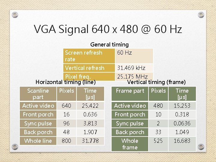
VGA Signal 640 x 480 @ 60 Hz General timing Screen refresh rate 60 Hz Vertical refresh 31. 469 k. Hz Pixel freq. Horizontal timing (line) 25. 175 MHz Vertical timing (frame) Scanline part Pixels Time [μs] Frame part Pixels Time [μs] Active video 640 25. 422 Active video 480 15. 253 Front porch 16 0. 636 Front porch 10 0. 318 Sync pulse 96 3. 813 Sync pulse 2 0. 0636 Back porch 48 1. 907 Back porch 33 Whole line 800 31. 778 Whole frame 525 1. 049 7 16. 683 7

Hsync 640 16 96 48 Vsync Active video 480 10 2 33 VGA Signal 640 x 480 @ 60 Hz 8

VGA Signal 800 x 600 @ 60 Hz General timing Screen refresh rate 60 Hz Vertical refresh 37. 879 k. Hz Pixel freq. Horizontal timing (line) 40. 0 MHz Vertical timing (frame) Scanline part Pixels Time [μs] Frame part Pixels Time [μs] Active video 800 20 Active video 600 15. 84 Front porch 40 1 Front porch 1 0. 026 Sync pulse 128 3. 2 Sync pulse 4 0. 106 Back porch 88 2. 2 Back porch 23 Whole line 1056 26. 4 Whole frame 628 0. 607 9 16. 58 9

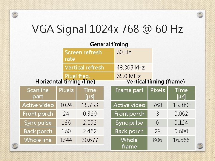
VGA Signal 1024 x 768 @ 60 Hz General timing Screen refresh rate 60 Hz Vertical refresh 48. 363 k. Hz Pixel freq. Horizontal timing (line) 65. 0 MHz Vertical timing (frame) Scanline part Pixels Time [μs] Frame part Pixels Time [μs] Active video 1024 15. 753 Active video 768 15. 880 Front porch 24 0. 369 Front porch 3 0. 062 Sync pulse 136 2. 092 Sync pulse 6 0. 124 Back porch 160 2. 462 Back porch 29 Whole line 1344 20. 677 Whole frame 806 0. 600 10 16. 666 10

VGA Signal 1280 x 1024 @ 60 Hz General timing Screen refresh rate 60 Hz Vertical refresh 63. 981 k. Hz Pixel freq. Horizontal timing (line) 108. 0 MHz Vertical timing (frame) Scanline part Pixels Time [μs] Frame part Pixels Time [μs] Active video 1280 11. 852 Active video 1024 16. 005 Front porch 48 0. 444 Front porch 1 0. 016 Sync pulse 112 1. 037 Sync pulse 3 0. 047 Back porch 248 2. 296 Back porch 38 Whole line 1688 15. 630 Whole frame 1066 0. 594 11 16. 661 11
![Pin Assignments Signal Name FPGA Pin No Description VGAR07 PINE 12H 10 VGA Red07 Pin Assignments Signal Name FPGA Pin No. Description VGA_R[0]~[7] PIN_E 12~H 10 VGA Red[0]~[7]](https://slidetodoc.com/presentation_image/1d0176ee4e1da90ca82ffc5e8c74d1b4/image-12.jpg)
Pin Assignments Signal Name FPGA Pin No. Description VGA_R[0]~[7] PIN_E 12~H 10 VGA Red[0]~[7] VGA_G[0]~[7] PIN_G 8~C 9 VGA Green[0]~[7] VGA_B[0]~[7] PIN_B 10~D 1 2 VGA Blue[0]~[7] VGA_CLK PIN_A 12 VGA CLOCK VGA_BLANK_N PIN_F 11 VGA BLANK VGA_HS PIN_G 13 VGA HSync VGA_VS PIN_C 13 VGA VSync VGA_SYNC_N PIN_C 10 Unused. Just assign 1. 0: Blank 1: Active data 12

The End. Any question?

Reference 1. http: //www- mtl. mit. edu/Courses/6. 111/labkit/vg a. shtml 2. http: //tinyvga. com/vga-timing 3. "DE 2 -115 User Manual" by Terasic. 14