Introduction to Verilog COE 203 Digital Logic Laboratory

Introduction to Verilog COE 203 Digital Logic Laboratory Dr. Aiman El-Maleh College of Computer Sciences and Engineering King Fahd University of Petroleum and Minerals
Outline … v Introduction v Why use HDL? v Definition of Module v Gate Level Modeling v Verilog Primitives v A Full Adder v 4 -bit Adder v Continuous Assignments v Behavioral Description of an Adder v Verilog Operators Introduction to Verilog COE 203 – Digital Design Lab – KFUPM slide 2
… Outline v Verilog Logic Values v Verilog Data Types v Always Block v Wire vs. Reg v If Statements v Case Statements v Sequential Circuits v Generalized Verilog Mealy Model v Generalized Verilog Moore Model v Finite State Machine Example Introduction to Verilog COE 203 – Digital Design Lab – KFUPM slide 3
Introduction v Verilog is one of the hardware description languages (HDL) available in the industry for hardware designing. v It allows designers to design at Behavior Level, Register Transfer Level (RTL), Gate level and at switch level. v Parallel not serial (Not like C language). v Verilog can describe everything from single gate to full computer system. Introduction to Verilog COE 203 – Digital Design Lab – KFUPM slide 4
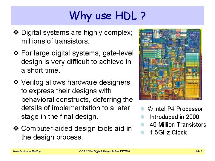
Why use HDL ? v Digital systems are highly complex; millions of transistors. v For large digital systems, gate-level design is very difficult to achieve in a short time. v Verilog allows hardware designers to express their designs with behavioral constructs, deferring the details of implementation to a later l © Intel P 4 Processor l Introduced in 2000 stage in the final design. v Computer-aided design tools aid in the design process. Introduction to Verilog COE 203 – Digital Design Lab – KFUPM l 40 Million Transistors l 1. 5 GHz Clock slide 5
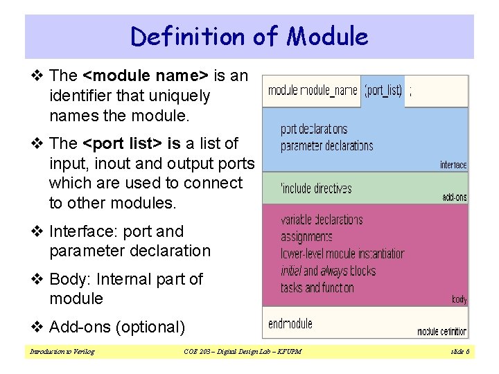
Definition of Module v The <module name> is an identifier that uniquely names the module. v The <port list> is a list of input, inout and output ports which are used to connect to other modules. v Interface: port and parameter declaration v Body: Internal part of module v Add-ons (optional) Introduction to Verilog COE 203 – Digital Design Lab – KFUPM slide 6
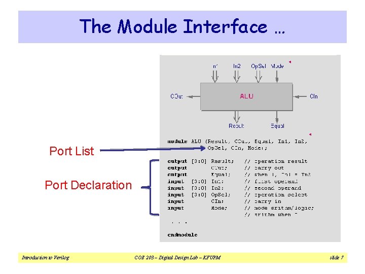
The Module Interface … Port List Port Declaration Introduction to Verilog COE 203 – Digital Design Lab – KFUPM slide 7
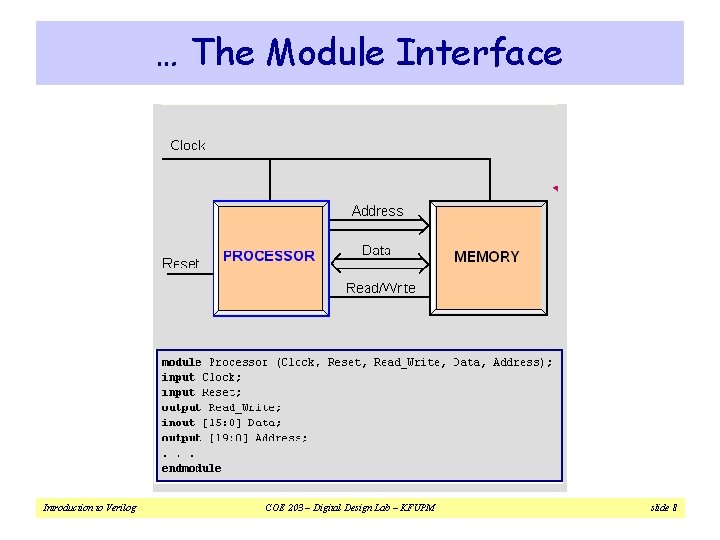
… The Module Interface Introduction to Verilog COE 203 – Digital Design Lab – KFUPM slide 8
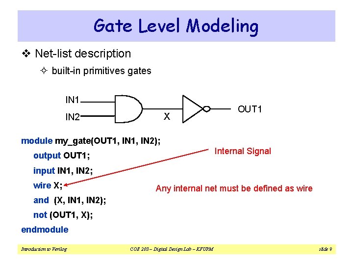
Gate Level Modeling v Net-list description ² built-in primitives gates IN 1 X IN 2 OUT 1 module my_gate(OUT 1, IN 2); Internal Signal output OUT 1; input IN 1, IN 2; wire X; Any internal net must be defined as wire and (X, IN 1, IN 2); not (OUT 1, X); endmodule Introduction to Verilog COE 203 – Digital Design Lab – KFUPM slide 9
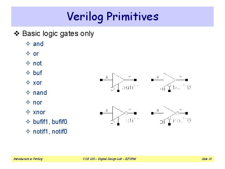
Verilog Primitives v Basic logic gates only ² and ² or ² not ² buf ² xor ² nand ² nor ² xnor ² bufif 1, bufif 0 ² notif 1, notif 0 Introduction to Verilog COE 203 – Digital Design Lab – KFUPM slide 10
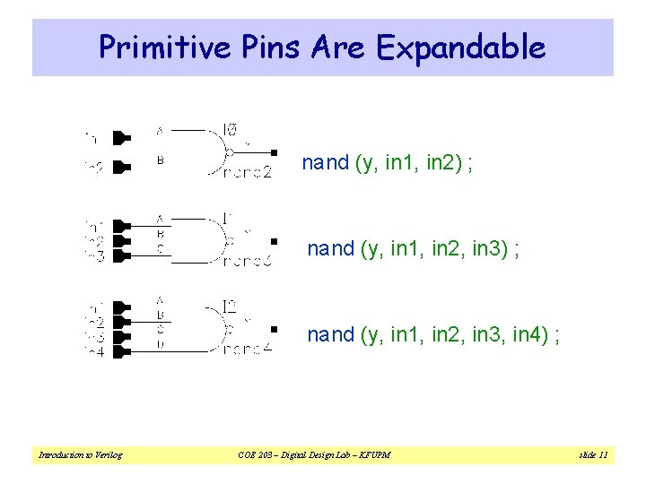
Primitive Pins Are Expandable nand (y, in 1, in 2) ; nand (y, in 1, in 2, in 3, in 4) ; Introduction to Verilog COE 203 – Digital Design Lab – KFUPM slide 11
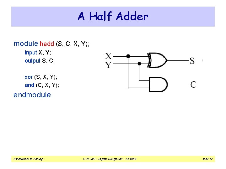
A Half Adder module hadd (S, C, X, Y); input X, Y; output S, C; xor (S, X, Y); and (C, X, Y); endmodule Introduction to Verilog COE 203 – Digital Design Lab – KFUPM slide 12
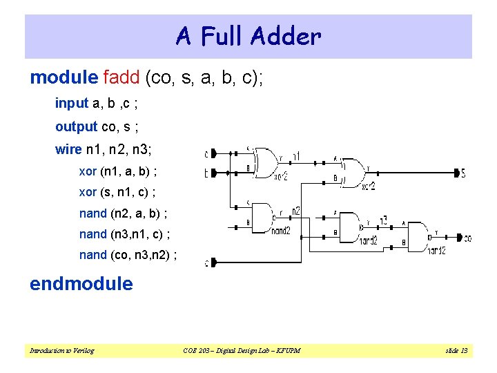
A Full Adder module fadd (co, s, a, b, c); input a, b , c ; output co, s ; wire n 1, n 2, n 3; xor (n 1, a, b) ; xor (s, n 1, c) ; nand (n 2, a, b) ; nand (n 3, n 1, c) ; nand (co, n 3, n 2) ; endmodule Introduction to Verilog COE 203 – Digital Design Lab – KFUPM slide 13
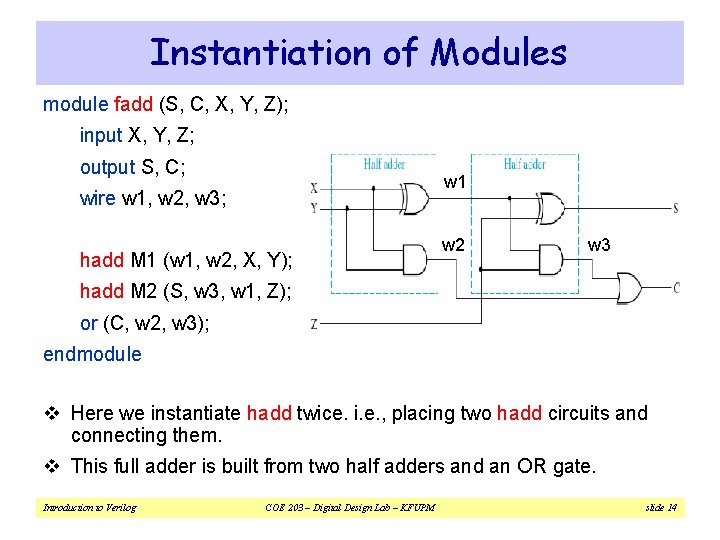
Instantiation of Modules module fadd (S, C, X, Y, Z); input X, Y, Z; output S, C; w 1 wire w 1, w 2, w 3; hadd M 1 (w 1, w 2, X, Y); w 2 w 3 hadd M 2 (S, w 3, w 1, Z); or (C, w 2, w 3); endmodule v Here we instantiate hadd twice. i. e. , placing two hadd circuits and connecting them. v This full adder is built from two half adders and an OR gate. Introduction to Verilog COE 203 – Digital Design Lab – KFUPM slide 14
![4 -bit Adder module add 4 (s, cout, ci, a, b); input [3: 0] 4 -bit Adder module add 4 (s, cout, ci, a, b); input [3: 0]](http://slidetodoc.com/presentation_image_h2/cee9f4606e4f55ad0bc59a4a4545a4b7/image-15.jpg)
4 -bit Adder module add 4 (s, cout, ci, a, b); input [3: 0] a, b ; // port declarations input ci ; output [3: 0] s ; output cout ; a[3] b[3] // vector cout wire [2: 0] co ; a[2] b[2] a[1] b[1] a[0] b[0] a 3 a 2 co[2] fadd a 0 (co[0], s[0], a[0], b[0], ci) ; s[3] a 1 co[1] s[2] a 0 co[0] s[1] s[0] fadd a 1 (co[1], s[1], a[1], b[1], co[0]) ; fadd a 2 (co[2], s[2], a[2], b[2], co[1]) ; fadd a 3 (cout, s[3], a[3], b[3], co[2]) ; endmodule Introduction to Verilog COE 203 – Digital Design Lab – KFUPM slide 15 ci
Continuous Assignments v Describe combinational logic v Operands + operators v Drive values to a net ² assign out = a&b ; // and gate ² assign eq = (a==b) ; // comparator ² wire #10 inv = ~in ; // inverter with delay ² wire [7: 0] c = a+b ; // 8 -bit adder v Avoid logic loops ² assign a = b + a ; ² asynchronous design Introduction to Verilog COE 203 – Digital Design Lab – KFUPM slide 16
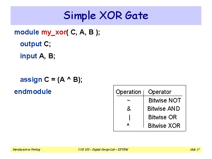
Simple XOR Gate module my_xor( C, A, B ); output C; input A, B; assign C = (A ^ B); endmodule Introduction to Verilog Operation Operator ~ Bitwise NOT & Bitwise AND | Bitwise OR ^ Bitwise XOR COE 203 – Digital Design Lab – KFUPM slide 17
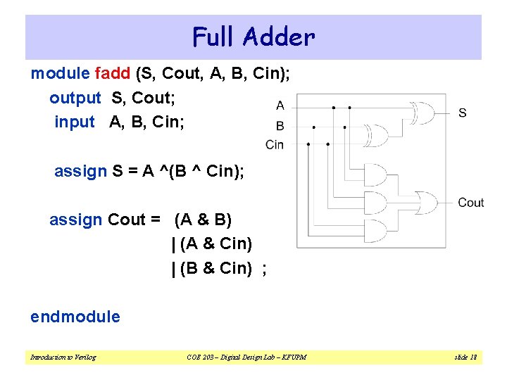
Full Adder module fadd (S, Cout, A, B, Cin); output S, Cout; input A, B, Cin; assign S = A ^(B ^ Cin); assign Cout = (A & B) | (A & Cin) | (B & Cin) ; endmodule Introduction to Verilog COE 203 – Digital Design Lab – KFUPM slide 18
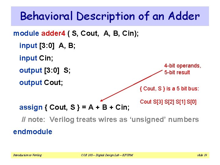
Behavioral Description of an Adder module adder 4 ( S, Cout, A, B, Cin); input [3: 0] A, B; input Cin; 4 -bit operands, 5 -bit result output [3: 0] S; output Cout; { Cout, S } is a 5 bit bus: assign { Cout, S } = A + B + Cin; Cout S[3] S[2] S[1] S[0] // note: Verilog treats wires as ‘unsigned’ numbers endmodule Introduction to Verilog COE 203 – Digital Design Lab – KFUPM slide 19
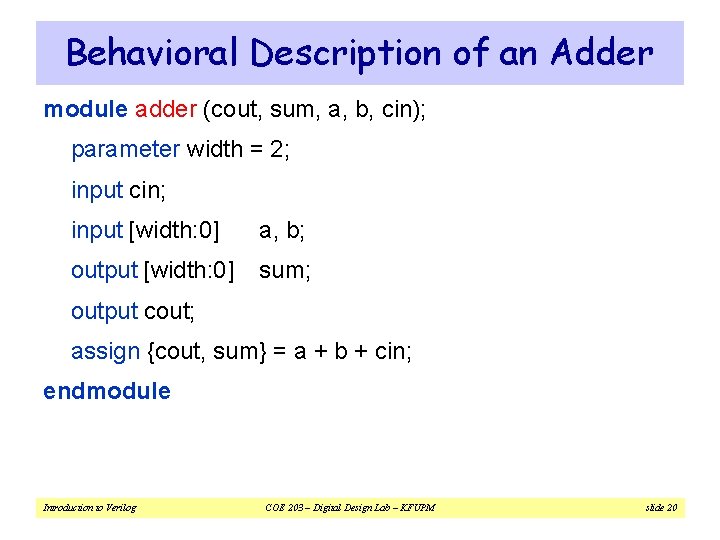
Behavioral Description of an Adder module adder (cout, sum, a, b, cin); parameter width = 2; input cin; input [width: 0] a, b; output [width: 0] sum; output cout; assign {cout, sum} = a + b + cin; endmodule Introduction to Verilog COE 203 – Digital Design Lab – KFUPM slide 20
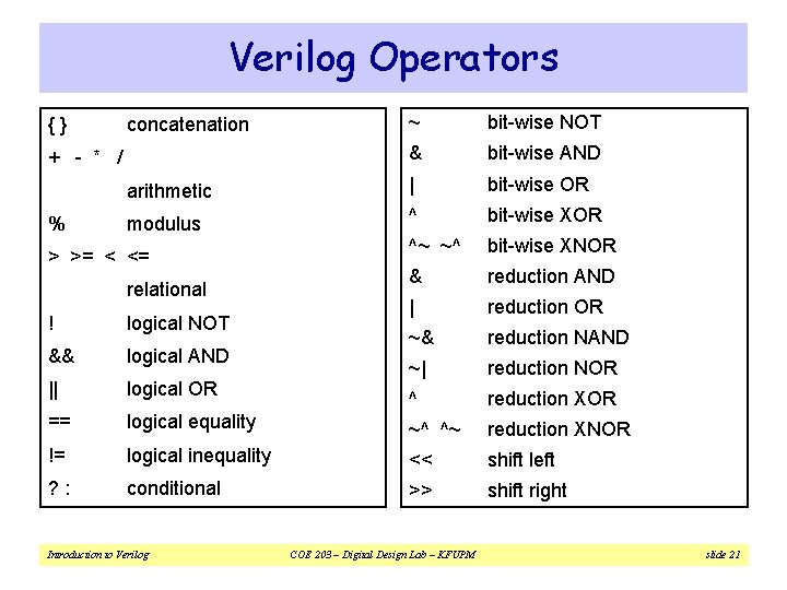
Verilog Operators {} ~ bit-wise NOT & bit-wise AND arithmetic | bit-wise OR modulus ^ bit-wise XOR ^~ ~^ bit-wise XNOR & reduction AND | reduction OR ~& reduction NAND ~| reduction NOR ^ reduction XOR concatenation + - * / % > >= < <= relational ! logical NOT && logical AND || logical OR == logical equality ~^ ^~ reduction XNOR != logical inequality << shift left ? : conditional >> shift right Introduction to Verilog COE 203 – Digital Design Lab – KFUPM slide 21
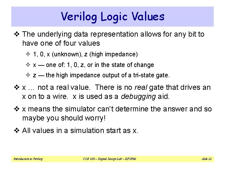
Verilog Logic Values v The underlying data representation allows for any bit to have one of four values ² 1, 0, x (unknown), z (high impedance) ² x — one of: 1, 0, z, or in the state of change ² z — the high impedance output of a tri-state gate. v x … not a real value. There is no real gate that drives an x on to a wire. x is used as a debugging aid. v x means the simulator can’t determine the answer and so maybe you should worry! v All values in a simulation start as x. Introduction to Verilog COE 203 – Digital Design Lab – KFUPM slide 22
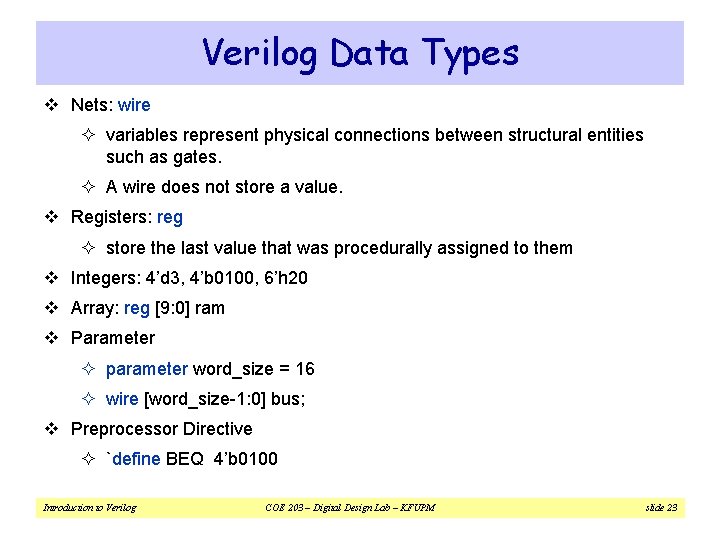
Verilog Data Types v Nets: wire ² variables represent physical connections between structural entities such as gates. ² A wire does not store a value. v Registers: reg ² store the last value that was procedurally assigned to them v Integers: 4’d 3, 4’b 0100, 6’h 20 v Array: reg [9: 0] ram v Parameter ² parameter word_size = 16 ² wire [word_size-1: 0] bus; v Preprocessor Directive ² `define BEQ 4’b 0100 Introduction to Verilog COE 203 – Digital Design Lab – KFUPM slide 23
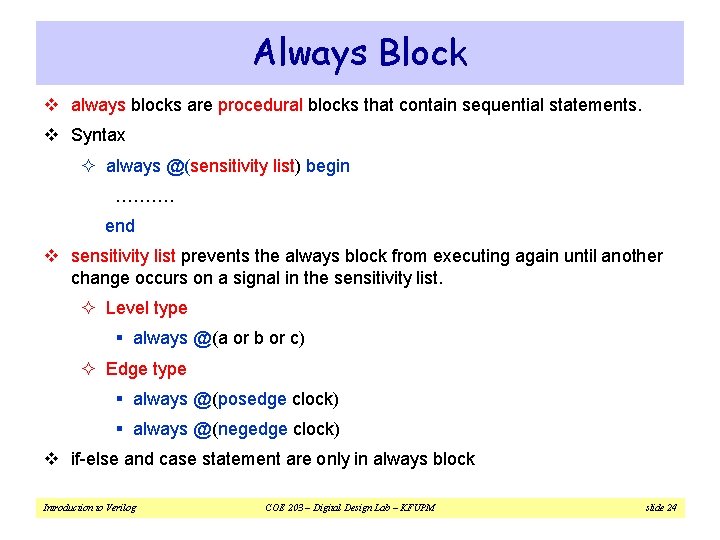
Always Block v always blocks are procedural blocks that contain sequential statements. v Syntax ² always @(sensitivity list) begin ………. end v sensitivity list prevents the always block from executing again until another change occurs on a signal in the sensitivity list. ² Level type § always @(a or b or c) ² Edge type § always @(posedge clock) § always @(negedge clock) v if-else and case statement are only in always block Introduction to Verilog COE 203 – Digital Design Lab – KFUPM slide 24
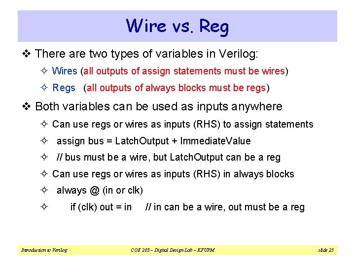
Wire vs. Reg v There are two types of variables in Verilog: ² Wires (all outputs of assign statements must be wires) ² Regs (all outputs of always blocks must be regs) v Both variables can be used as inputs anywhere ² Can use regs or wires as inputs (RHS) to assign statements ² assign bus = Latch. Output + Immediate. Value ² // bus must be a wire, but Latch. Output can be a reg ² Can use regs or wires as inputs (RHS) in always blocks ² always @ (in or clk) ² Introduction to Verilog if (clk) out = in // in can be a wire, out must be a reg COE 203 – Digital Design Lab – KFUPM slide 25
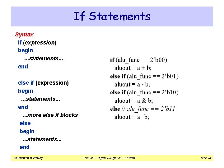
If Statements Syntax if (expression) begin. . . statements. . . end else if (expression) begin. . . statements. . . end. . . more else if blocks else begin. . . statements. . . end Introduction to Verilog COE 203 – Digital Design Lab – KFUPM slide 26
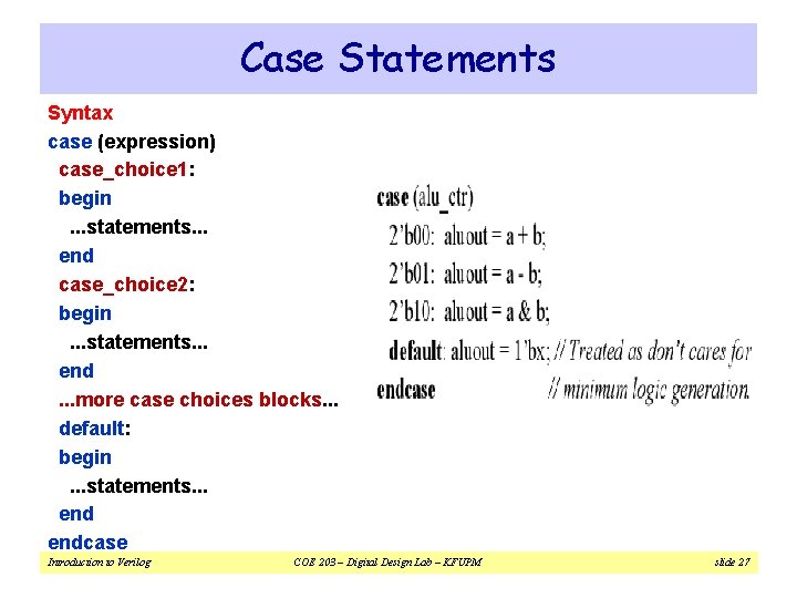
Case Statements Syntax case (expression) case_choice 1: begin. . . statements. . . end case_choice 2: begin. . . statements. . . end. . . more case choices blocks. . . default: begin. . . statements. . . endcase Introduction to Verilog COE 203 – Digital Design Lab – KFUPM slide 27
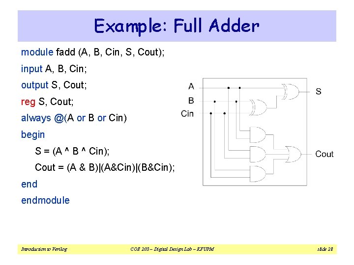
Example: Full Adder module fadd (A, B, Cin, S, Cout); input A, B, Cin; output S, Cout; reg S, Cout; always @(A or B or Cin) begin S = (A ^ B ^ Cin); Cout = (A & B)|(A&Cin)|(B&Cin); endmodule Introduction to Verilog COE 203 – Digital Design Lab – KFUPM slide 28
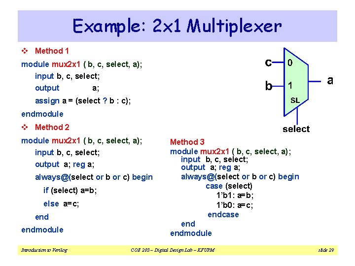
Example: 2 x 1 Multiplexer v Method 1 module mux 2 x 1 ( b, c, select, a); input b, c, select; output a; assign a = (select ? b : c); endmodule v Method 2 module mux 2 x 1 ( b, c, select, a); input b, c, select; output a; reg a; always@(select or b or c) begin if (select) a=b; else a=c; endmodule Introduction to Verilog Method 3 module mux 2 x 1 ( b, c, select, a); input b, c, select; output a; reg a; always@(select or b or c) begin case (select) 1’b 1: a=b; 1’b 0: a=c; endcase endmodule COE 203 – Digital Design Lab – KFUPM slide 29
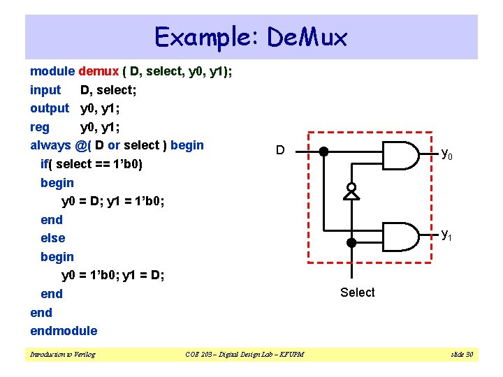
Example: De. Mux module demux ( D, select, y 0, y 1); input D, select; output y 0, y 1; reg y 0, y 1; always @( D or select ) begin if( select == 1’b 0) begin y 0 = D; y 1 = 1’b 0; end else begin y 0 = 1’b 0; y 1 = D; end endmodule Introduction to Verilog D COE 203 – Digital Design Lab – KFUPM y 0 y 1 Select slide 30
![Example: Arithmetic Unit module arithmetic (A, B, Y, Sel); parameter width=3; input [width-1: 0] Example: Arithmetic Unit module arithmetic (A, B, Y, Sel); parameter width=3; input [width-1: 0]](http://slidetodoc.com/presentation_image_h2/cee9f4606e4f55ad0bc59a4a4545a4b7/image-31.jpg)
Example: Arithmetic Unit module arithmetic (A, B, Y, Sel); parameter width=3; input [width-1: 0] A, B; input [1: 0] Sel; output [width-1: 0] Y; reg [width-1: 0] Y; always @(A or B or Sel) begin case (Sel[1: 0]) 2'b 00 : Y = A+B; 2'b 01 : Y = A-B; 2'b 10 : Y = A+1; 2'b 11 : Y = A-1; default: Y=0; endcase endmodule Introduction to Verilog COE 203 – Digital Design Lab – KFUPM slide 31
![Example: Logic Unit module logic (A, B, Y, Sel); parameter width=2; input [width-1: 0] Example: Logic Unit module logic (A, B, Y, Sel); parameter width=2; input [width-1: 0]](http://slidetodoc.com/presentation_image_h2/cee9f4606e4f55ad0bc59a4a4545a4b7/image-32.jpg)
Example: Logic Unit module logic (A, B, Y, Sel); parameter width=2; input [width-1: 0] A, B; input [2: 0] Sel; output [width-1: 0] Y; reg [width-1: 0] Y; always @(A or B or Sel) begin case (Sel[2: 0]) 3'b 000 : Y = A & B; // A and B 3'b 001 : Y = A | B; // A or B 3'b 010 : Y = A ^ B; // A xor B 3'b 011 : Y = ~A; // 1’s complement of A 3'b 100 : Y = ~(A & B); // A nand B 3'b 101 : Y = ~(A | B); // A nor B default : Y = 0; endcase endmodule Introduction to Verilog COE 203 – Digital Design Lab – KFUPM slide 32
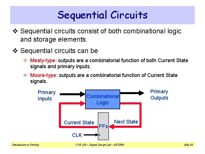
Sequential Circuits v Sequential circuits consist of both combinational logic and storage elements. v Sequential circuits can be ² Mealy-type: outputs are a combinatorial function of both Current State signals and primary inputs. ² Moore-type: outputs are a combinatorial function of Current State signals. Primary Inputs Combinational Logic Current State Introduction to Verilog Next State ^ CLK FFs Primary Outputs COE 203 – Digital Design Lab – KFUPM slide 33
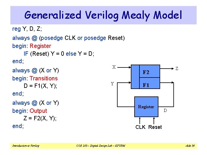
Generalized Verilog Mealy Model reg Y, D, Z; always @ (posedge CLK or posedge Reset) begin: Register IF (Reset) Y = 0 else Y = D; end; always @ (X or Y) begin: Transitions D = F 1(X, Y); end; X Y always @ (X or Y) begin: Output Z = F 2(X, Y); end; Introduction to Verilog Z F 2 F 1 Register D CLK Reset COE 203 – Digital Design Lab – KFUPM slide 34
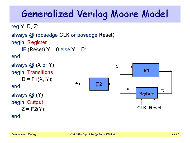
Generalized Verilog Moore Model reg Y, D, Z; always @ (posedge CLK or posedge Reset) begin: Register IF (Reset) Y = 0 else Y = D; end; always @ (X or Y) begin: Transitions D = F 1(X, Y); end; X Z F 2 Y always @ (Y) begin: Output Z = F 2(Y); end; Introduction to Verilog F 1 Register D CLK Reset COE 203 – Digital Design Lab – KFUPM slide 35
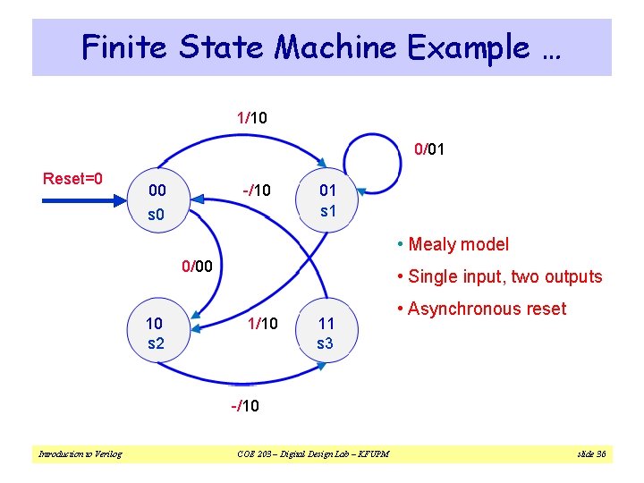
Finite State Machine Example … 1/10 0/01 Reset=0 00 s 0 -/10 01 s 1 • Mealy model 0/00 10 s 2 • Single input, two outputs 1/10 11 s 3 • Asynchronous reset -/10 Introduction to Verilog COE 203 – Digital Design Lab – KFUPM slide 36
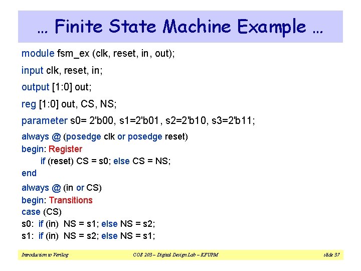
… Finite State Machine Example … module fsm_ex (clk, reset, in, out); input clk, reset, in; output [1: 0] out; reg [1: 0] out, CS, NS; parameter s 0= 2'b 00, s 1=2'b 01, s 2=2'b 10, s 3=2'b 11; always @ (posedge clk or posedge reset) begin: Register if (reset) CS = s 0; else CS = NS; end always @ (in or CS) begin: Transitions case (CS) s 0: if (in) NS = s 1; else NS = s 2; s 1: if (in) NS = s 2; else NS = s 1; Introduction to Verilog COE 203 – Digital Design Lab – KFUPM slide 37
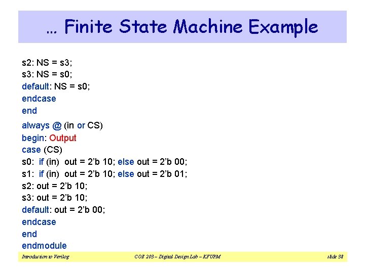
… Finite State Machine Example s 2: NS = s 3; s 3: NS = s 0; default: NS = s 0; endcase end always @ (in or CS) begin: Output case (CS) s 0: if (in) out = 2’b 10; else out = 2’b 00; s 1: if (in) out = 2’b 10; else out = 2’b 01; s 2: out = 2’b 10; s 3: out = 2’b 10; default: out = 2’b 00; endcase endmodule Introduction to Verilog COE 203 – Digital Design Lab – KFUPM slide 38
- Slides: 38