Introduction to semiconductor technology Outline 4 Excitation of
- Slides: 26

Introduction to semiconductor technology

Outline – 4 Excitation of semiconductors • • Optical absorption and excitation Luminescence Recombination Diffusion of charge carriers

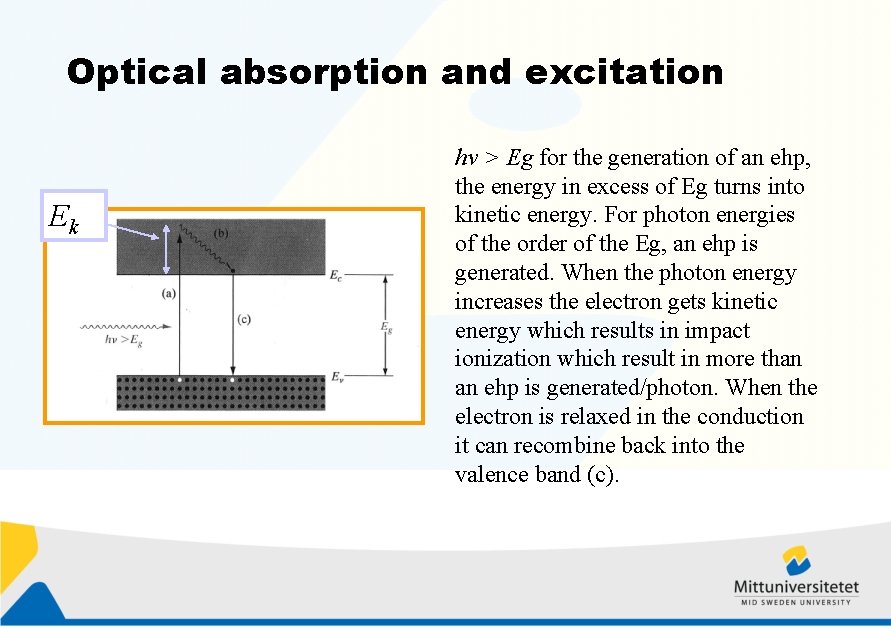
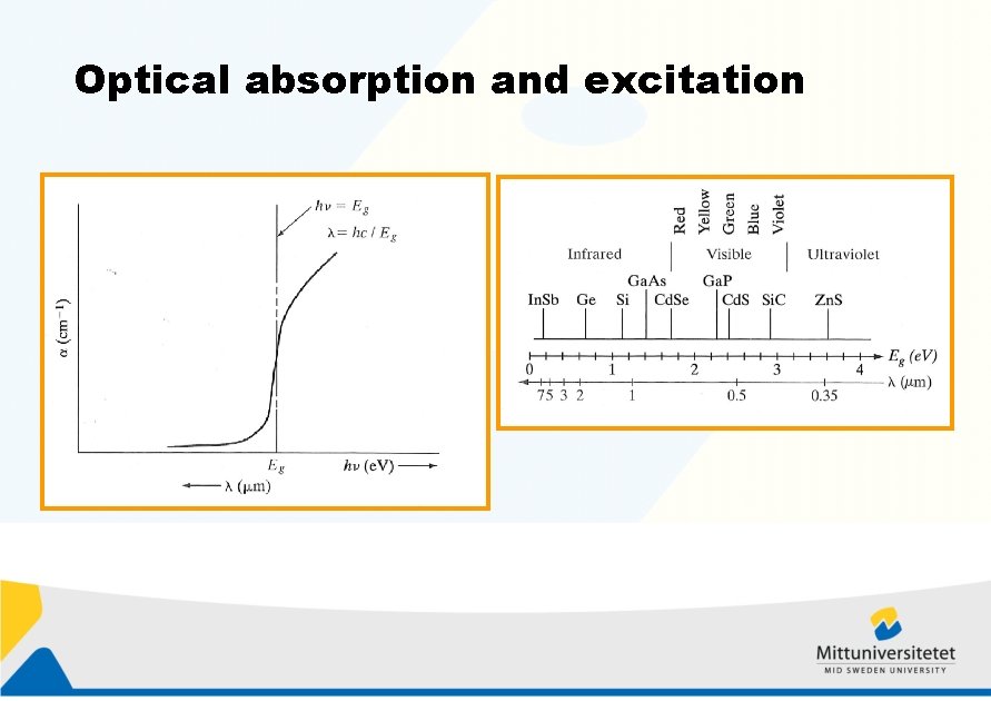
Optical absorption and excitation Ek hv > Eg for the generation of an ehp, the energy in excess of Eg turns into kinetic energy. For photon energies of the order of the Eg, an ehp is generated. When the photon energy increases the electron gets kinetic energy which results in impact ionization which result in more than an ehp is generated/photon. When the electron is relaxed in the conduction it can recombine back into the valence band (c).

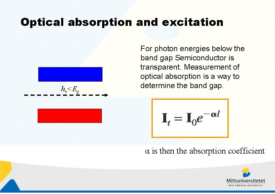
Optical absorption and excitation hv<Eg For photon energies below the band gap Semiconductor is transparent. Measurement of optical absorption is a way to determine the band gap. α is then the absorption coefficient

Optical absorption and excitation

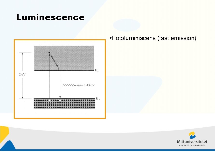
Luminescence • Fotoluminiscens (fast emission)

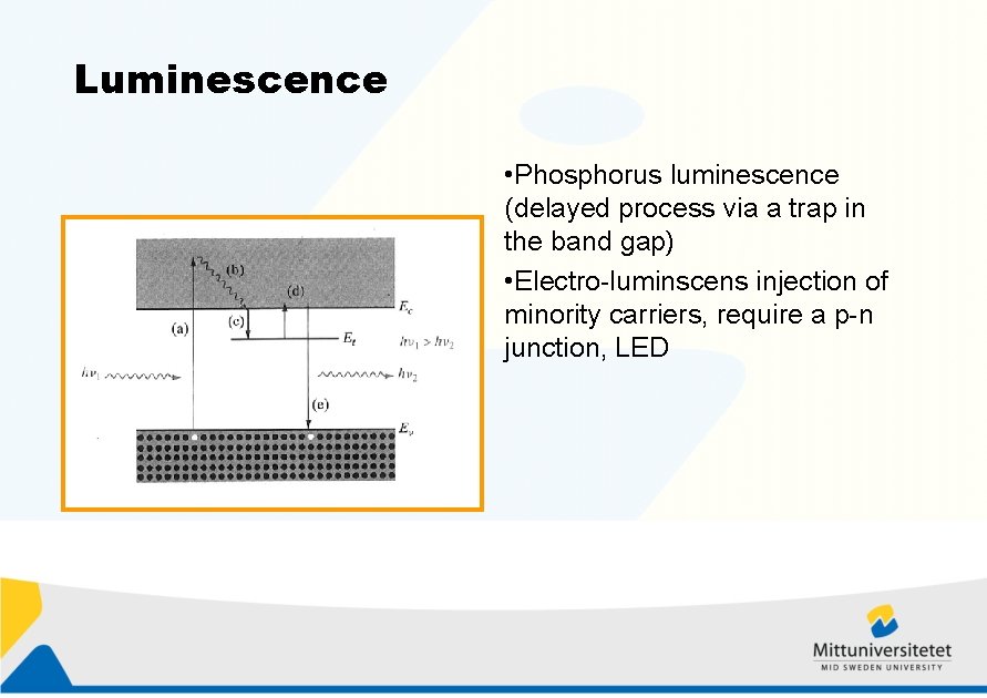
Luminescence • Phosphorus luminescence (delayed process via a trap in the band gap) • Electro-luminscens injection of minority carriers, require a p-n junction, LED

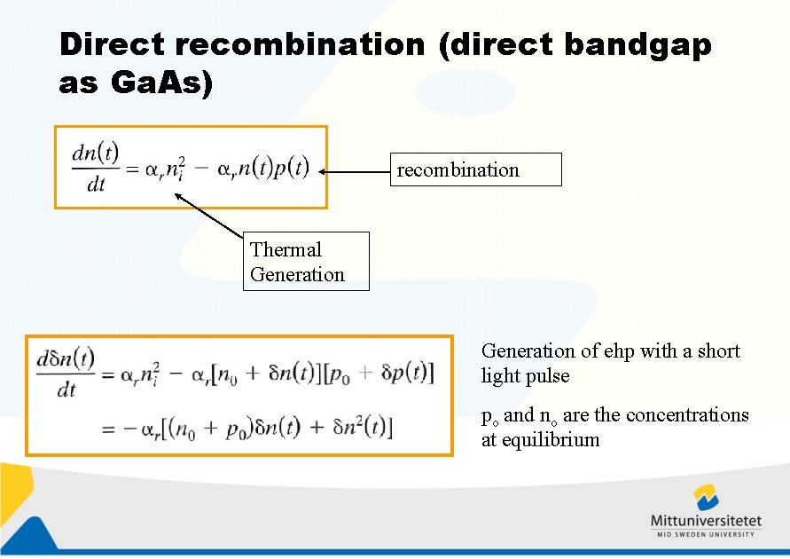
Direct recombination (direct bandgap as Ga. As) recombination Thermal Generation of ehp with a short light pulse po and no are the concentrations at equilibrium

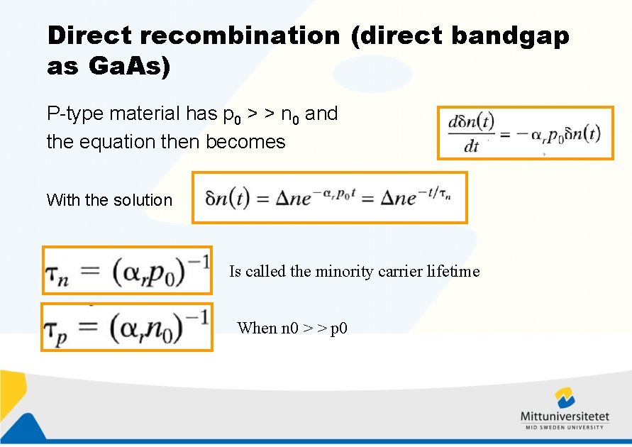
Direct recombination (direct bandgap as Ga. As) P-type material has p 0 > > n 0 and the equation then becomes With the solution Is called the minority carrier lifetime When n 0 > > p 0

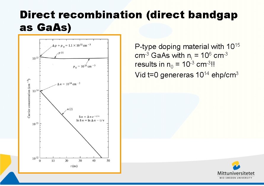
Direct recombination (direct bandgap as Ga. As) P-type doping material with 1015 cm-3 Ga. As with ni = 106 cm-3 results in n 0 = 10 -3 cm-3!! Vid t=0 genereras 1014 ehp/cm 3

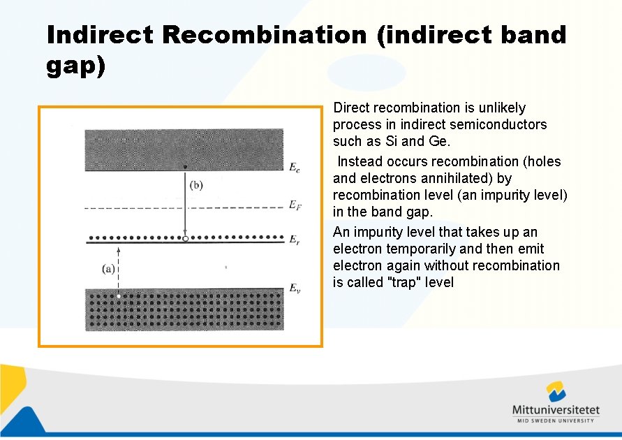
Indirect Recombination (indirect band gap) Direct recombination is unlikely process in indirect semiconductors such as Si and Ge. Instead occurs recombination (holes and electrons annihilated) by recombination level (an impurity level) in the band gap. An impurity level that takes up an electron temporarily and then emit electron again without recombination is called "trap" level

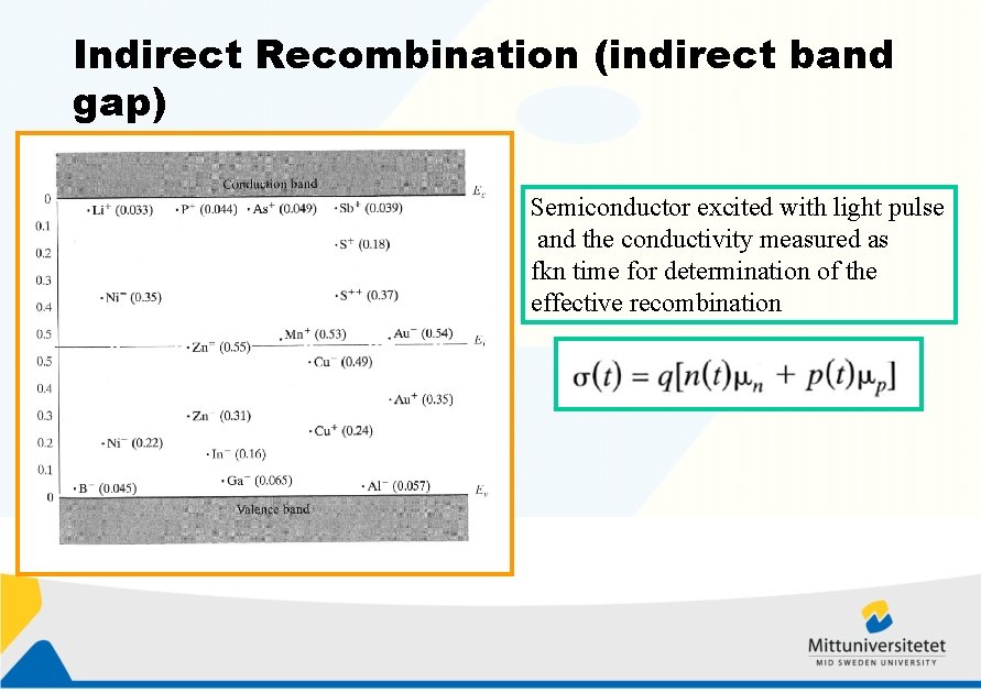
Indirect Recombination (indirect band gap) Semiconductor excited with light pulse and the conductivity measured as fkn time for determination of the effective recombination

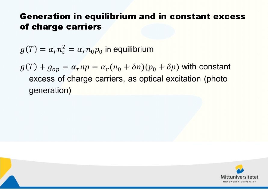
Generation in equilibrium and in constant excess of charge carriers

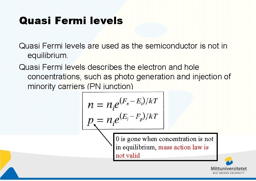
Quasi Fermi levels are used as the semiconductor is not in equilibrium. Quasi Fermi levels describes the electron and hole concentrations, such as photo generation and injection of minority carriers (PN junction) 0 is gone when concentration is not in equilibrium, mass action law is not valid

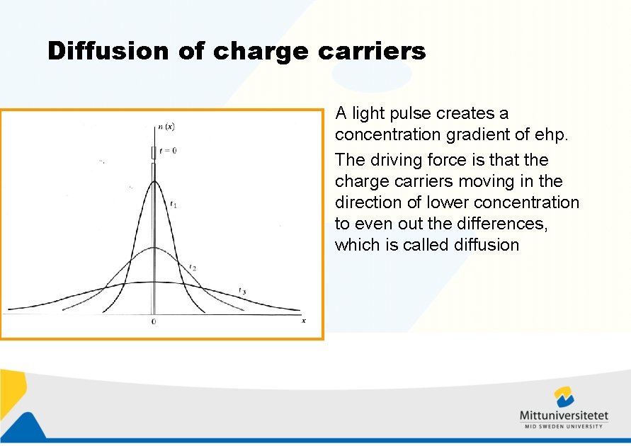
Diffusion of charge carriers A light pulse creates a concentration gradient of ehp. The driving force is that the charge carriers moving in the direction of lower concentration to even out the differences, which is called diffusion

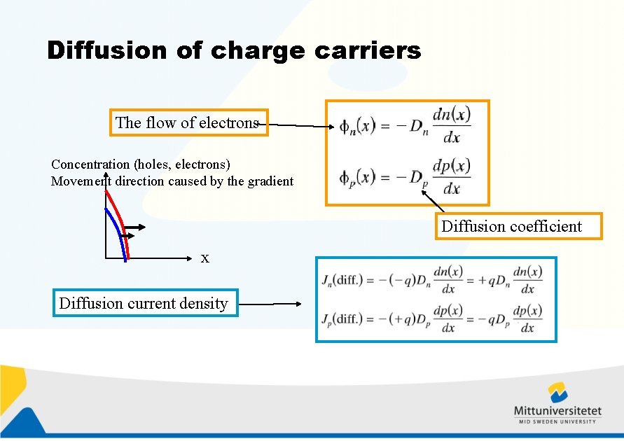
Diffusion of charge carriers The flow of electrons Concentration (holes, electrons) Movement direction caused by the gradient Diffusion coefficient x Diffusion current density

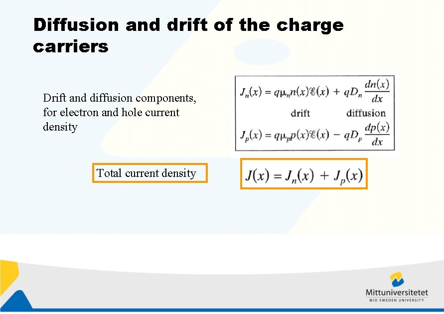
Diffusion and drift of the charge carriers Drift and diffusion components, for electron and hole current density Total current density

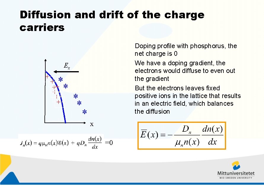
Diffusion and drift of the charge carriers Doping profile with phosphorus, the net charge is 0 We have a doping gradient, the electrons would diffuse to even out the gradient But the electrons leaves fixed positive ions in the lattice that results in an electric field, which balances the diffusion Ex + * * + ++ + * * * x =0

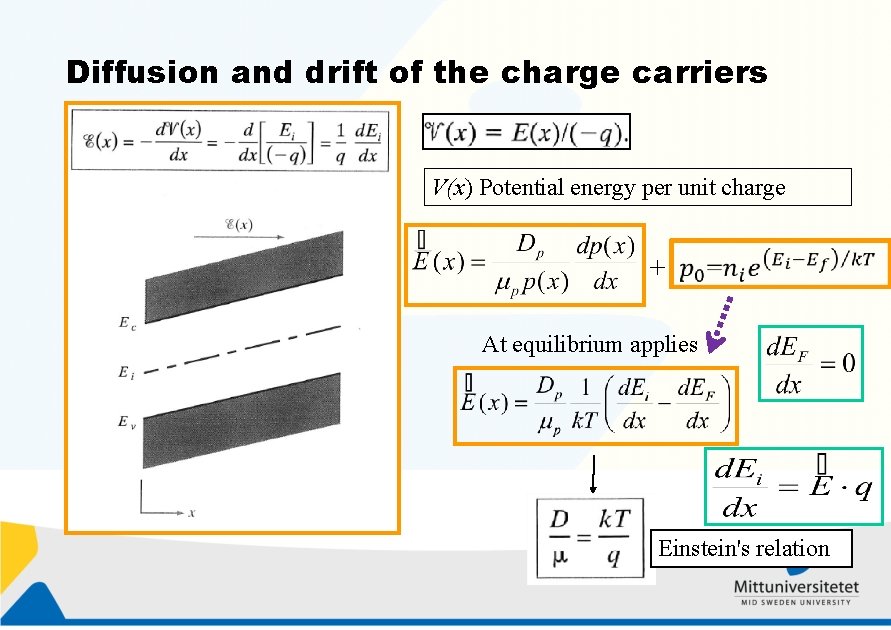
Diffusion and drift of the charge carriers V(x) Potential energy per unit charge + At equilibrium applies Einstein's relation

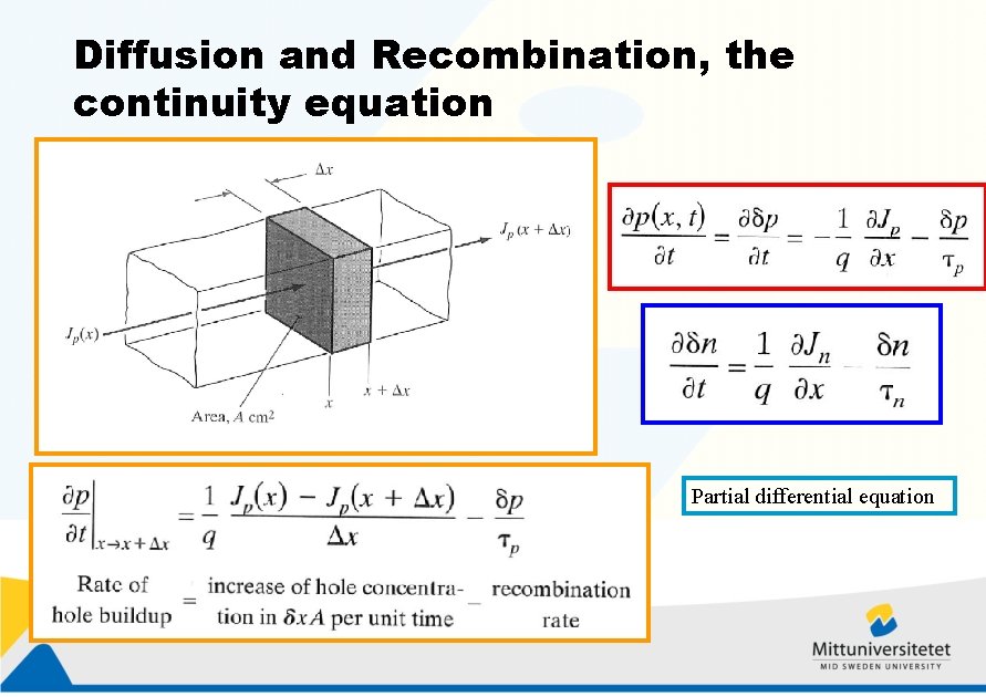
Diffusion and Recombination, the continuity equation Partial differential equation

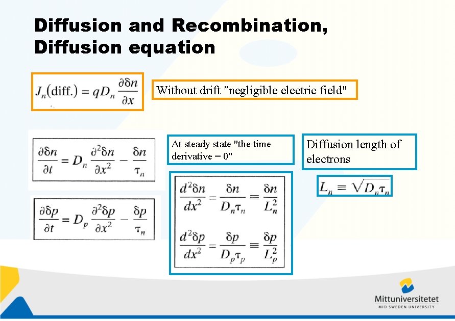
Diffusion and Recombination, Diffusion equation Without drift "negligible electric field" At steady state "the time derivative = 0" Diffusion length of electrons

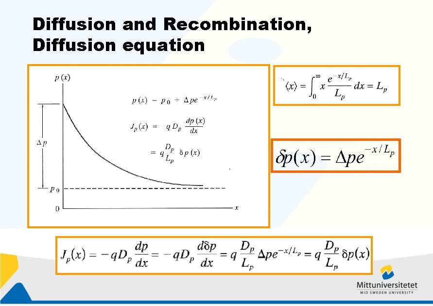
Diffusion and Recombination, Diffusion equation

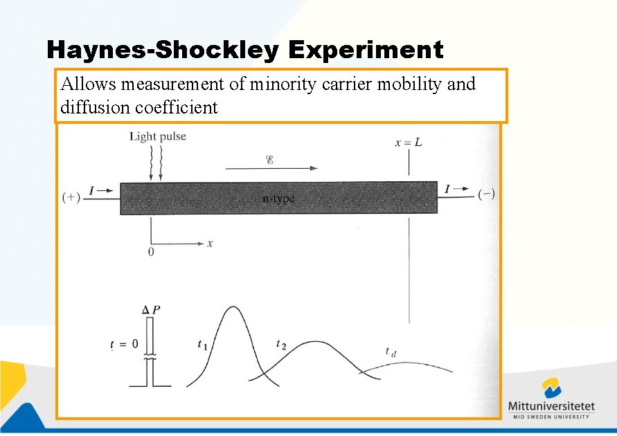
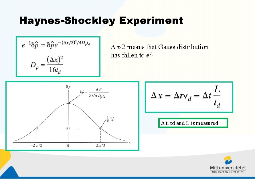
Haynes-Shockley Experiment Allows measurement of minority carrier mobility and diffusion coefficient

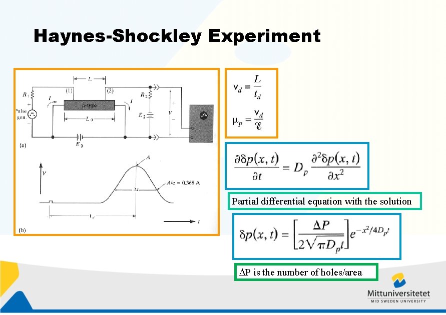
Haynes-Shockley Experiment Partial differential equation with the solution P is the number of holes/area

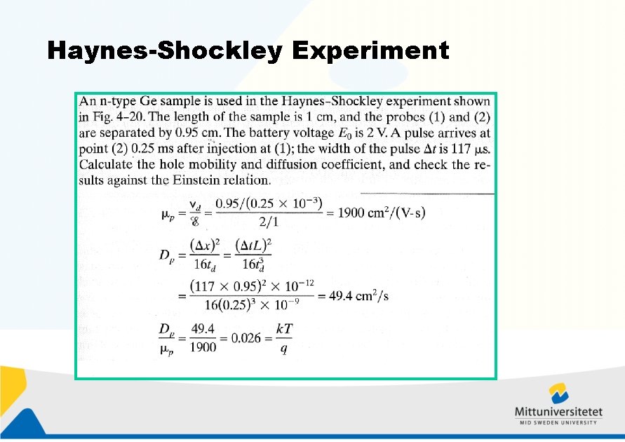
Haynes-Shockley Experiment ∆ x/2 means that Gauss distribution has fallen to e-1 t, td and L is measured

Haynes-Shockley Experiment