INTRODUCTION TO PIC MICROCONTROLLER Overview and Features The

- Slides: 16

INTRODUCTION TO PIC MICROCONTROLLER

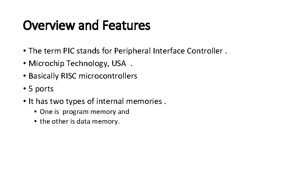
Overview and Features • The term PIC stands for Peripheral Interface Controller. • Microchip Technology, USA. • Basically RISC microcontrollers • 5 ports • It has two types of internal memories. • One is program memory and • the other is data memory.

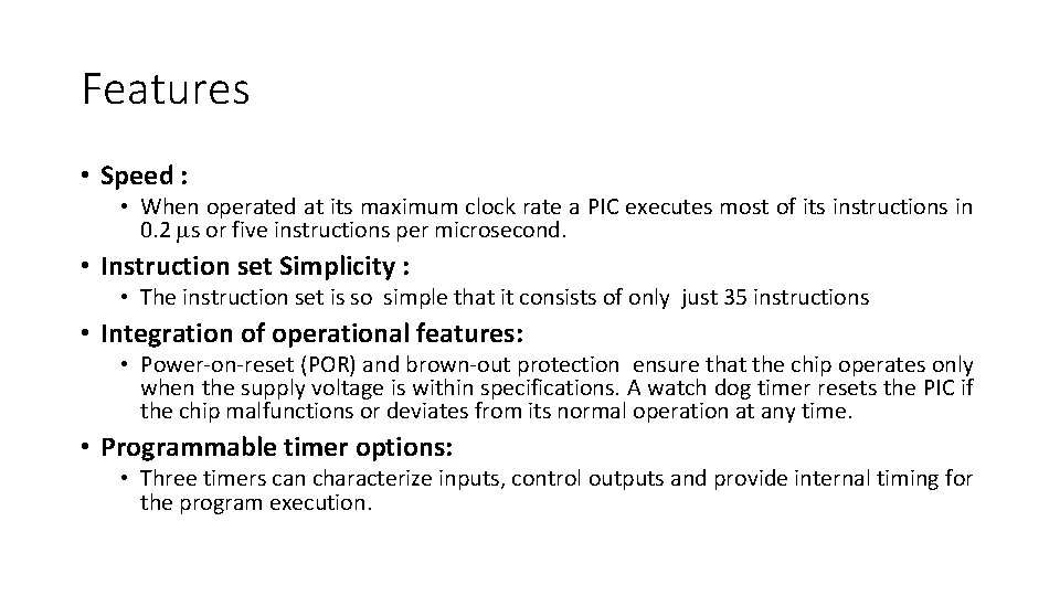
Features • Speed : • When operated at its maximum clock rate a PIC executes most of its instructions in 0. 2 s or five instructions per microsecond. • Instruction set Simplicity : • The instruction set is so simple that it consists of only just 35 instructions • Integration of operational features: • Power-on-reset (POR) and brown-out protection ensure that the chip operates only when the supply voltage is within specifications. A watch dog timer resets the PIC if the chip malfunctions or deviates from its normal operation at any time. • Programmable timer options: • Three timers can characterize inputs, control outputs and provide internal timing for the program execution.

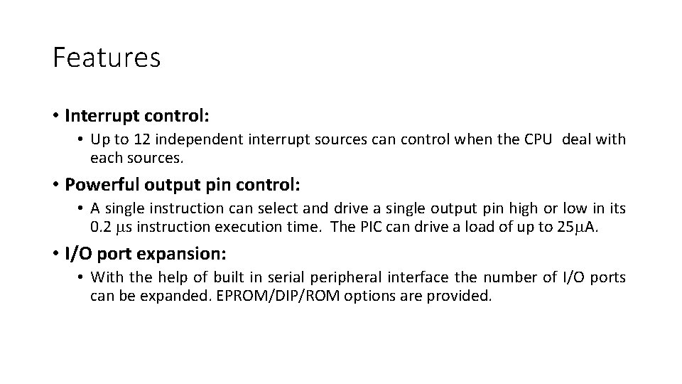
Features • Interrupt control: • Up to 12 independent interrupt sources can control when the CPU deal with each sources. • Powerful output pin control: • A single instruction can select and drive a single output pin high or low in its 0. 2 s instruction execution time. The PIC can drive a load of up to 25 A. • I/O port expansion: • With the help of built in serial peripheral interface the number of I/O ports can be expanded. EPROM/DIP/ROM options are provided.

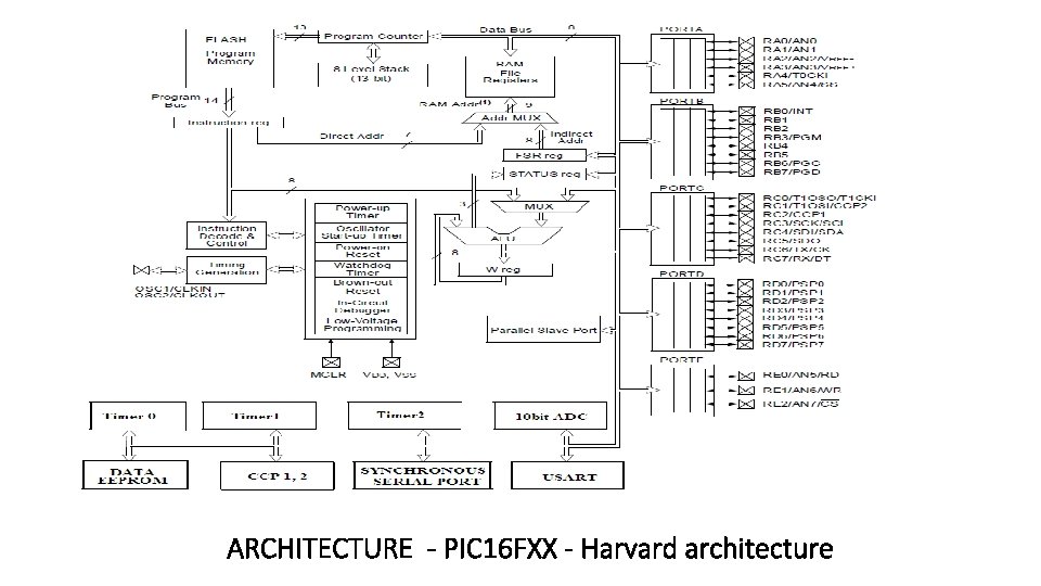
ARCHITECTURE - PIC 16 FXX - Harvard architecture

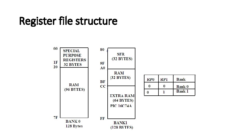
Memory organization and register file structure The memory module of the PICcontroller has three memory blocks. • Program memory • Data memory and Stack REGISTER FILE STRUCTURE In PIC Microcontrollers the Register File consists of two parts namely • General Purpose Register File • Special Purpose Register File

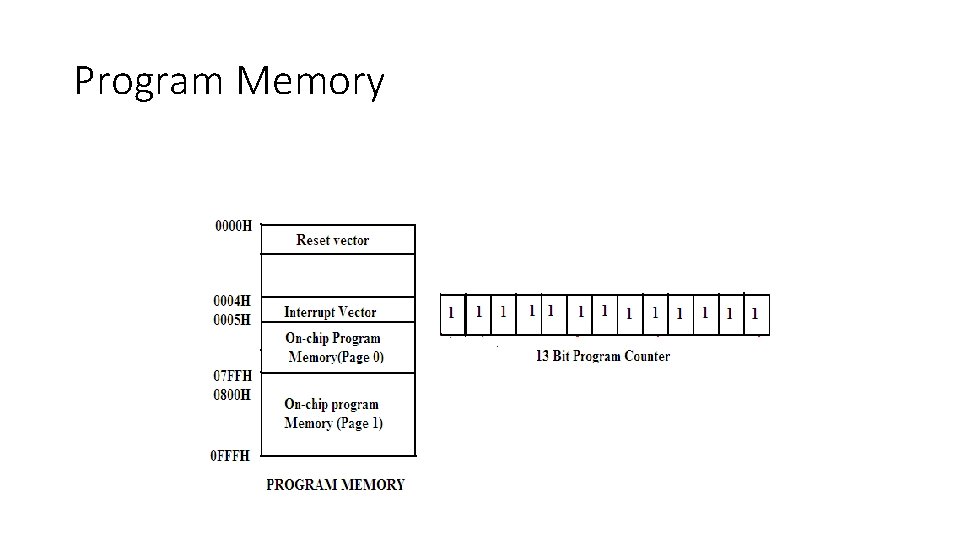
Program Memory

DATA MEMORY • The data memory of PIC 16 F 8 XX is partitioned into multiple banks which contain the general purpose registers and the Special function Registers. (SFRs). • The bits RP 1 and RP 0 bits of the status register are used to select these banks. • Each bank extends upto 7 FH(128 Bytes). • The lower bytes of the each bank are reserved for the Special Function Registers. • Above the SFRs are general purpose registers implemented as static RAM.

Register file structure General Purpose Register File: • The general purpose register file is another name for the microcontroller’s RAM. • Data can be written to each 8 -bit location updated and retrieved any number of times. Special Purpose Register File: • The special function register file consists of input, output ports and control registers used to configure each 8 -bit port either as input or output. • It contains registers that provide the data input and data output to a chip resources like Timers, Serial Ports and Analog to Digital converter • the registers that contains control bits for selecting the mode of operation and also enabling or disabling its operation.

Register file structure

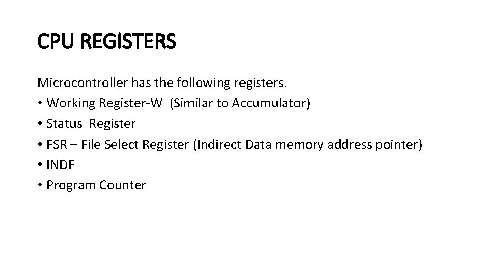
CPU REGISTERS Microcontroller has the following registers. • Working Register-W (Similar to Accumulator) • Status Register • FSR – File Select Register (Indirect Data memory address pointer) • INDF • Program Counter

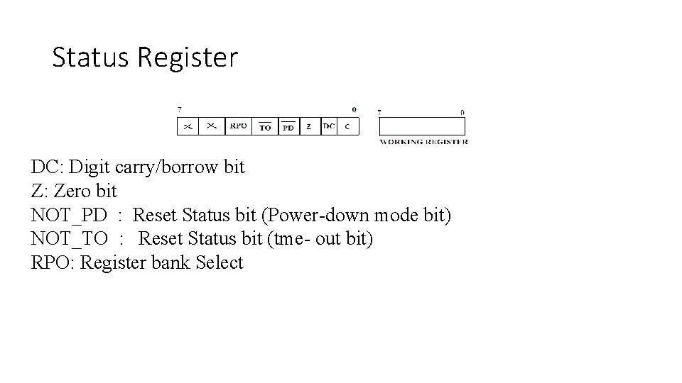
Status Register DC: Digit carry/borrow bit Z: Zero bit NOT_PD : Reset Status bit (Power-down mode bit) NOT_TO : Reset Status bit (tme- out bit) RPO: Register bank Select

FSR – (File Select Register) • It is the pointer used for indirect addressing. • In the indirect addressing mode the 8 -bit register file address is first written into FSR. • It is a special purpose register that serves as an address pointer to any address through out the entire register file.

INDF – (Indirect File): • It is not a physical register addressing but this INDF will cause indirect addressing. • Any instruction using the INDF register actually access the register pointed to by the FSR.

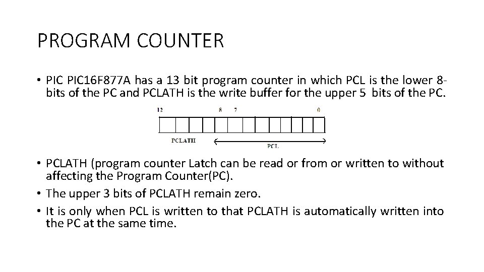
PROGRAM COUNTER • PIC 16 F 877 A has a 13 bit program counter in which PCL is the lower 8 bits of the PC and PCLATH is the write buffer for the upper 5 bits of the PC. • PCLATH (program counter Latch can be read or from or written to without affecting the Program Counter(PC). • The upper 3 bits of PCLATH remain zero. • It is only when PCL is written to that PCLATH is automatically written into the PC at the same time.

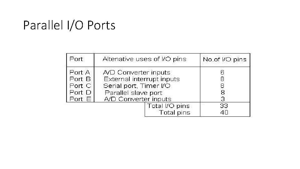
Parallel I/O Ports