Introduction to Microstrip Antennas David R Jackson Dept






- Slides: 179

Introduction to Microstrip Antennas David R. Jackson Dept. of ECE University of Houston 1

Contact Information David R. Jackson Dept. of ECE N 308 Engineering Building 1 University of Houston, TX 77204 -4005 Phone: 713 -743 -4426 Fax: 713 -743 -4444 Email: djackson@uh. edu 2

Purpose of Short Course § Provide an introduction to microstrip antennas. § Provide a physical and mathematical basis for understanding how microstrip antennas work. § Provide a physical understanding of the basic physical properties of microstrip antennas. § Provide an overview of some of the recent advances and trends in the area (but not an exhaustive survey – directed towards understanding the fundamental principles). 3

Additional Resources § Some basic references are provided at the end of these viewgraphs. § You are welcome to visit a website that goes along with a course at the University of Houston on microstrip antennas (Power. Point viewgraphs from the course may be found there, along with the viewgraphs from this short course). ECE 6345: Microstrip Antennas http: //courses. egr. uh. edu/ECE 6345/ Note: You are welcome to use anything that you find on this website, as long as you please acknowledge the source. 4

Outline v Overview of microstrip antennas v Feeding methods v Basic principles of operation v General characteristics v CAD Formulas v Input Impedance v Radiation pattern v Circular polarization v Circular patch v Improving bandwidth v Miniaturization v Reducing surface waves and lateral radiation 5

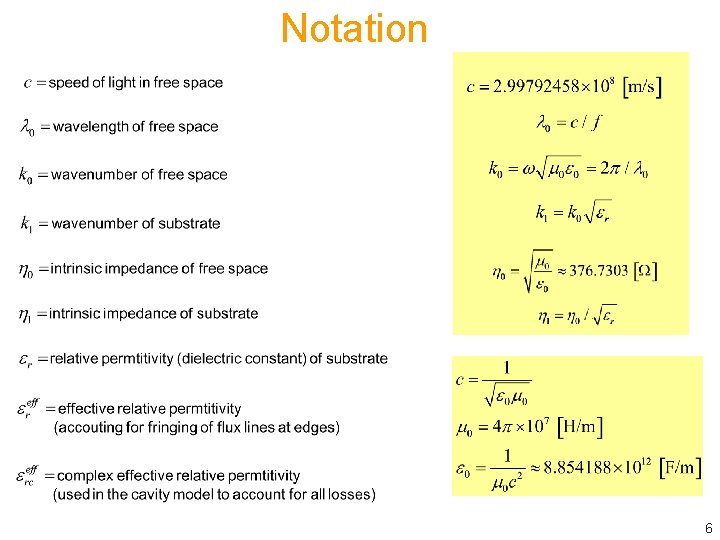
Notation 6

Outline v Overview of microstrip antennas v Feeding methods v Basic principles of operation v General characteristics v CAD Formulas v Input Impedance v Radiation pattern v Circular polarization v Circular patch v Improving bandwidth v Miniaturization v Reducing surface waves and lateral radiation 7

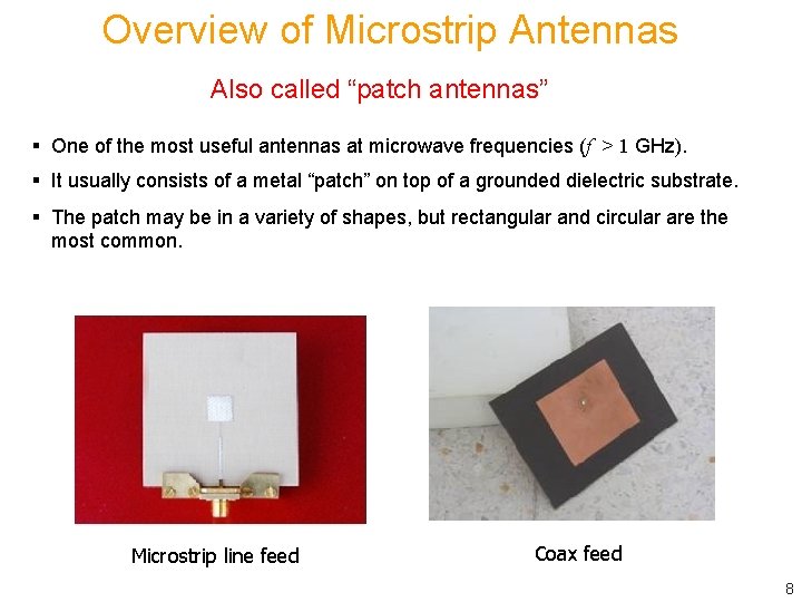
Overview of Microstrip Antennas Also called “patch antennas” § One of the most useful antennas at microwave frequencies (f > 1 GHz). § It usually consists of a metal “patch” on top of a grounded dielectric substrate. § The patch may be in a variety of shapes, but rectangular and circular are the most common. Microstrip line feed Coax feed 8

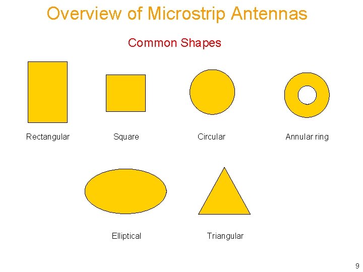
Overview of Microstrip Antennas Common Shapes Rectangular Square Elliptical Circular Annular ring Triangular 9

Overview of Microstrip Antennas History § Invented by Bob Munson in 1972 (but earlier work by Dechamps goes back to 1953). § Became popular starting in the 1970 s. G. Deschamps and W. Sichak, “Microstrip Microwave Antennas, ” Proc. of Third Symp. on USAF Antenna Research and Development Program, October 18– 22, 1953. R. E. Munson, “Microstrip Phased Array Antennas, ” Proc. of Twenty-Second Symp. on USAF Antenna Research and Development Program, October 1972. R. E. Munson, “Conformal Microstrip Antennas and Microstrip Phased Arrays, ” IEEE Trans. Antennas Propagat. , vol. AP-22, no. 1 (January 1974): 74– 78. 10

Overview of Microstrip Antennas Advantages of Microstrip Antennas Ø Low profile (can even be “conformal, ” i. e. flexible to conform to a surface). Ø Easy to fabricate (use etching and photolithography). Ø Easy to feed (coaxial cable, microstrip line, etc. ). Ø Easy to incorporate with other microstrip circuit elements and integrate into systems. Ø Patterns are somewhat hemispherical, with a moderate directivity (about 6 -8 d. B is typical). Ø Easy to use in an array to increase the directivity. 11

Overview of Microstrip Antennas Disadvantages of Microstrip Antennas Ø Low bandwidth (but can be improved by a variety of techniques). Bandwidths of a few percent are typical. Bandwidth is roughly proportional to the substrate thickness and inversely proportional to the substrate permittivity. Ø Efficiency may be lower than with other antennas. Efficiency is limited by conductor and dielectric losses*, and by surface-wave loss**. Ø Only used at microwave frequencies and above (the substrate becomes too large at lower frequencies). Ø Cannot handle extremely large amounts of power (dielectric breakdown). * Conductor and dielectric losses become more severe for thinner substrates. ** Surface-wave losses become more severe for thicker substrates (unless air or foam is used). 12

Overview of Microstrip Antennas Applications include: § Satellite communications § Microwave communications § Cell phone antennas § GPS antennas 13

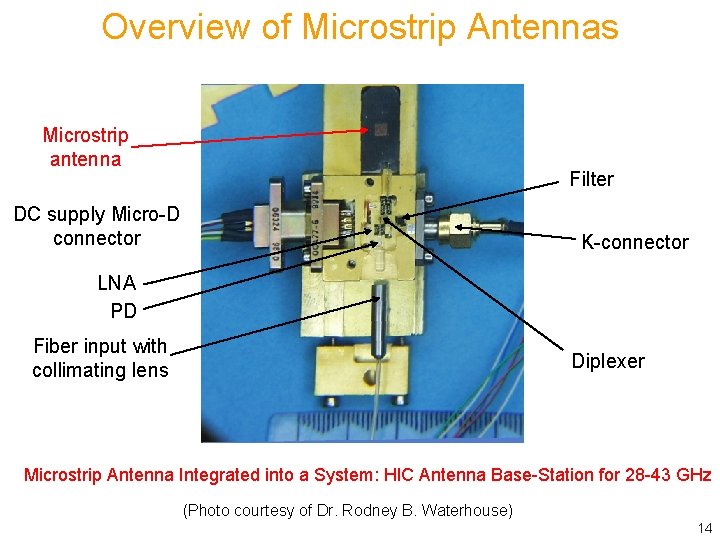
Overview of Microstrip Antennas Microstrip antenna Filter DC supply Micro-D connector K-connector LNA PD Fiber input with collimating lens Diplexer Microstrip Antenna Integrated into a System: HIC Antenna Base-Station for 28 -43 GHz (Photo courtesy of Dr. Rodney B. Waterhouse) 14

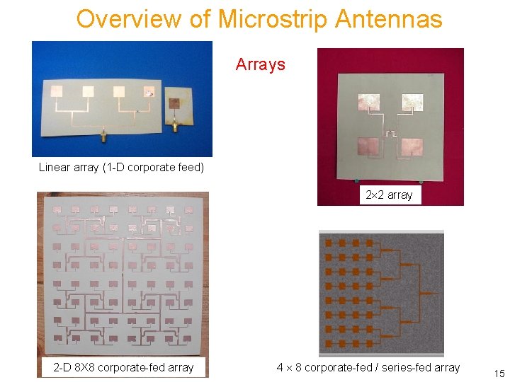
Overview of Microstrip Antennas Arrays Linear array (1 -D corporate feed) 2 2 array 2 -D 8 X 8 corporate-fed array 4 8 corporate-fed / series-fed array 15

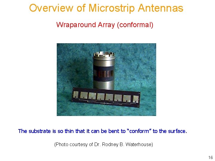
Overview of Microstrip Antennas Wraparound Array (conformal) The substrate is so thin that it can be bent to “conform” to the surface. (Photo courtesy of Dr. Rodney B. Waterhouse) 16

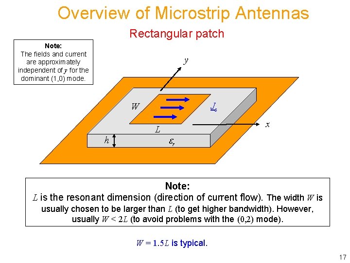
Overview of Microstrip Antennas Rectangular patch Note: The fields and current are approximately independent of y for the dominant (1, 0) mode. y Js W h L x r Note: L is the resonant dimension (direction of current flow). The width W is usually chosen to be larger than L (to get higher bandwidth). However, usually W < 2 L (to avoid problems with the (0, 2) mode). W = 1. 5 L is typical. 17

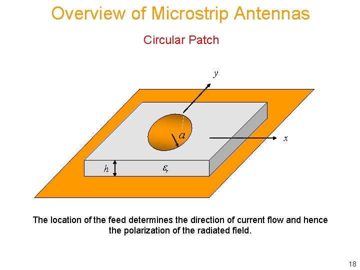
Overview of Microstrip Antennas Circular Patch y a h x r The location of the feed determines the direction of current flow and hence the polarization of the radiated field. 18

Outline v Overview of microstrip antennas v Feeding methods v Basic principles of operation v General characteristics v CAD Formulas v Input Impedance v Radiation pattern v Circular polarization v Circular patch v Improving bandwidth v Miniaturization v Reducing surface waves and lateral radiation 19

Feeding Methods Some of the more common methods for feeding microstrip antennas are shown. The feeding methods are illustrated for a rectangular patch, but the principles apply for circular and other shapes as well. 20

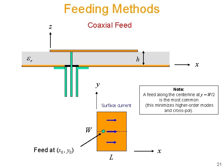
Feeding Methods z Coaxial Feed x y Surface current Note: A feed along the centerline at y = W/2 is the most common (this minimizes higher-order modes and cross-pol). W Feed at (x 0, y 0) L x 21

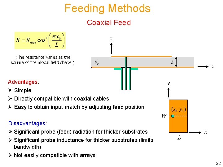
Feeding Methods Coaxial Feed z (The resistance varies as the square of the modal field shape. ) x Advantages: y Ø Simple Ø Directly compatible with coaxial cables Ø Easy to obtain input match by adjusting feed position W Disadvantages: Ø Significant probe (feed) radiation for thicker substrates Ø Significant probe inductance for thicker substrates (limits bandwidth) Ø Not easily compatible with arrays L x 22

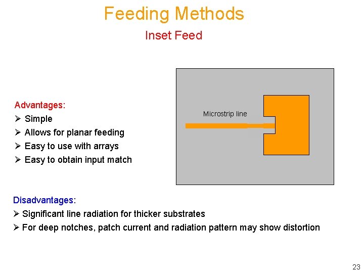
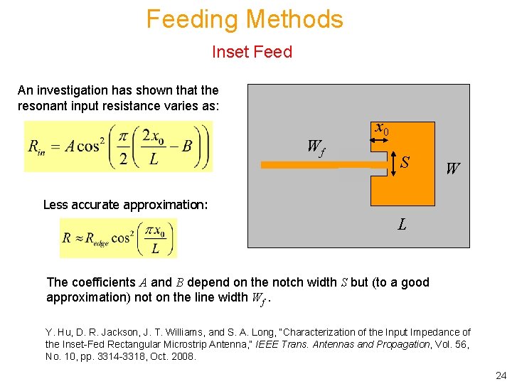
Feeding Methods Inset Feed Advantages: Ø Simple Ø Allows for planar feeding Ø Easy to use with arrays Ø Easy to obtain input match Microstrip line Disadvantages: Ø Significant line radiation for thicker substrates Ø For deep notches, patch current and radiation pattern may show distortion 23

Feeding Methods Inset Feed An investigation has shown that the resonant input resistance varies as: Wf x 0 S W Less accurate approximation: L The coefficients A and B depend on the notch width S but (to a good approximation) not on the line width Wf. Y. Hu, D. R. Jackson, J. T. Williams, and S. A. Long, “Characterization of the Input Impedance of the Inset-Fed Rectangular Microstrip Antenna, ” IEEE Trans. Antennas and Propagation, Vol. 56, No. 10, pp. 3314 -3318, Oct. 2008. 24

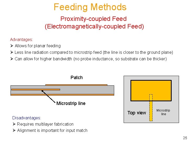
Feeding Methods Proximity-coupled Feed (Electromagnetically-coupled Feed) Advantages: Ø Allows for planar feeding Ø Less line radiation compared to microstrip feed (the line is closer to the ground plane) Ø Can allow for higher bandwidth (no probe inductance, so substrate can be thicker) Patch Microstrip line Top view Disadvantages: Ø Requires multilayer fabrication Ø Alignment is important for input match Microstrip line 25

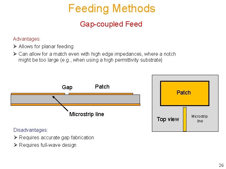
Feeding Methods Gap-coupled Feed Advantages: Ø Allows for planar feeding Ø Can allow for a match even with high edge impedances, where a notch might be too large (e. g. , when using a high permittivity substrate) Gap Patch Microstrip line Patch Top view Microstrip line Disadvantages: Ø Requires accurate gap fabrication Ø Requires full-wave design 26

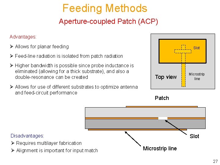
Feeding Methods Aperture-coupled Patch (ACP) Advantages: Ø Allows for planar feeding Slot Ø Feed-line radiation is isolated from patch radiation Ø Higher bandwidth is possible since probe inductance is eliminated (allowing for a thick substrate), and also a double-resonance can be created Ø Allows for use of different substrates to optimize antenna and feed-circuit performance Disadvantages: Ø Requires multilayer fabrication Ø Alignment is important for input match Top view Microstrip line Patch Slot Microstrip line 27

Outline v Overview of microstrip antennas v Feeding methods v Basic principles of operation v General characteristics v CAD Formulas v Input Impedance v Radiation pattern v Circular polarization v Circular patch v Improving bandwidth v Miniaturization v Reducing surface waves and lateral radiation 28

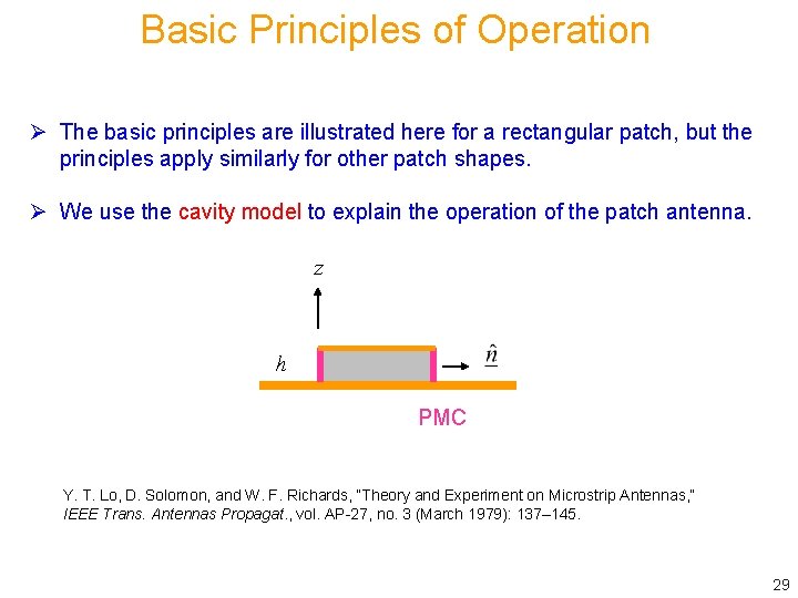
Basic Principles of Operation Ø The basic principles are illustrated here for a rectangular patch, but the principles apply similarly for other patch shapes. Ø We use the cavity model to explain the operation of the patch antenna. z h PMC Y. T. Lo, D. Solomon, and W. F. Richards, “Theory and Experiment on Microstrip Antennas, ” IEEE Trans. Antennas Propagat. , vol. AP-27, no. 3 (March 1979): 137– 145. 29

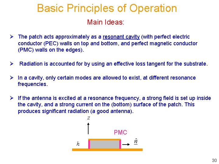
Basic Principles of Operation Main Ideas: Ø The patch acts approximately as a resonant cavity (with perfect electric conductor (PEC) walls on top and bottom, and perfect magnetic conductor (PMC) walls on the edges). Ø Radiation is accounted for by using an effective loss tangent for the substrate. Ø In a cavity, only certain modes are allowed to exist, at different resonance frequencies. Ø If the antenna is excited at a resonance frequency, a strong field is set up inside the cavity, and a strong current on the (bottom) surface of the patch. This produces significant radiation (a good antenna). z PMC h 30

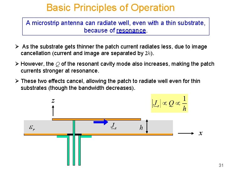
Basic Principles of Operation A microstrip antenna can radiate well, even with a thin substrate, because of resonance. Ø As the substrate gets thinner the patch current radiates less, due to image cancellation (current and image are separated by 2 h). Ø However, the Q of the resonant cavity mode also increases, making the patch currents stronger at resonance. Ø These two effects cancel, allowing the patch to radiate well even for thin substrates (though the bandwidth decreases). z x 31

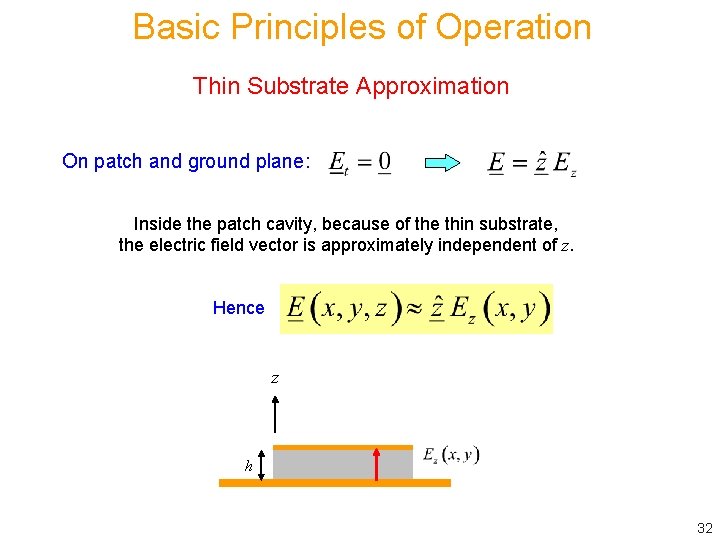
Basic Principles of Operation Thin Substrate Approximation On patch and ground plane: Inside the patch cavity, because of the thin substrate, the electric field vector is approximately independent of z. Hence z h 32

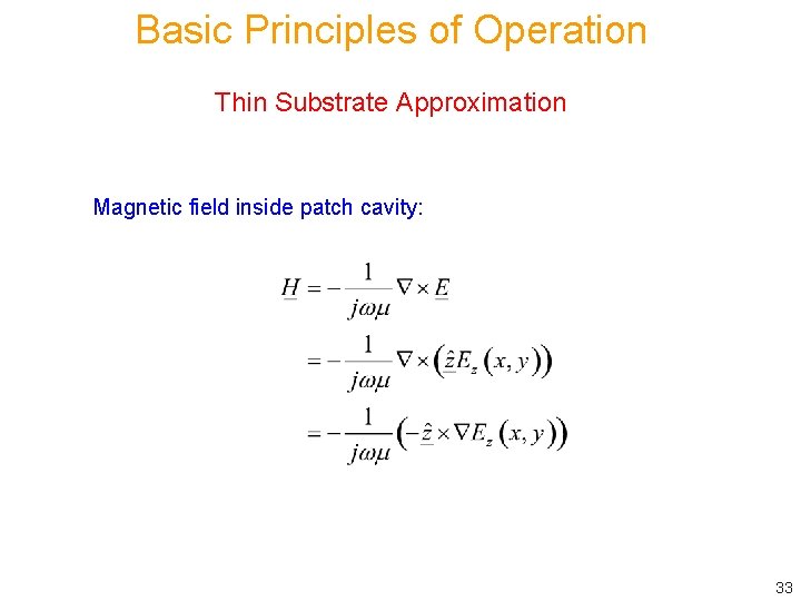
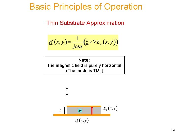
Basic Principles of Operation Thin Substrate Approximation Magnetic field inside patch cavity: 33

Basic Principles of Operation Thin Substrate Approximation Note: The magnetic field is purely horizontal. (The mode is TMz. ) z h 34

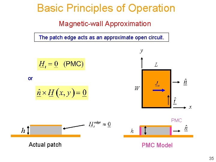
Basic Principles of Operation Magnetic-wall Approximation The patch edge acts as an approximate open circuit. y L or W x PMC h h Actual patch PMC Model 35

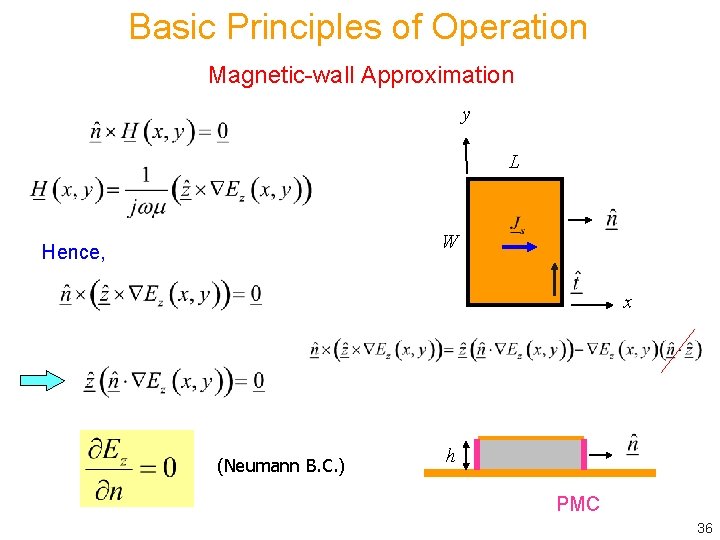
Basic Principles of Operation Magnetic-wall Approximation y L W Hence, x (Neumann B. C. ) h PMC 36

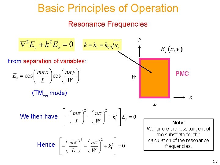
Basic Principles of Operation Resonance Frequencies y From separation of variables: PMC W (TMmn mode) L x We then have Hence Note: We ignore the loss tangent of the substrate for the calculation of the resonance frequencies. 37

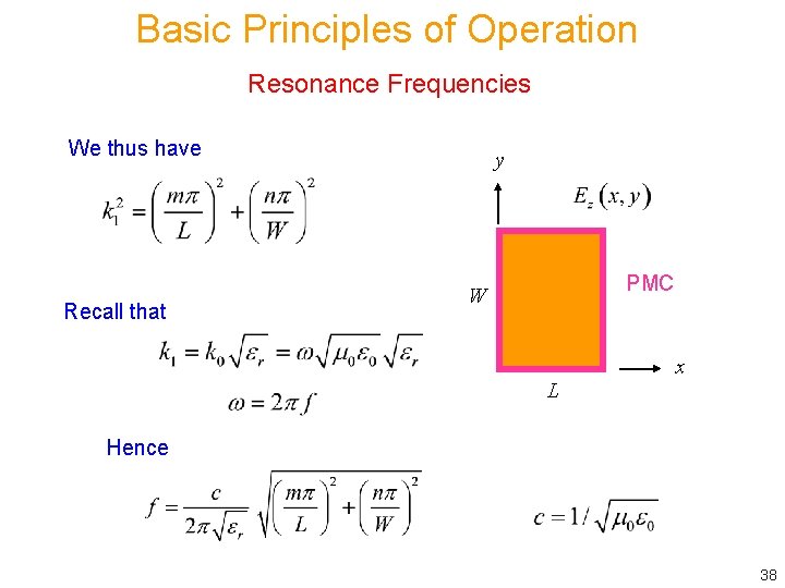
Basic Principles of Operation Resonance Frequencies We thus have Recall that y PMC W L x Hence 38

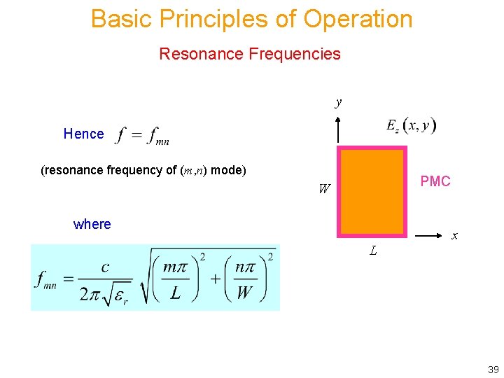
Basic Principles of Operation Resonance Frequencies y Hence (resonance frequency of (m, n) mode) PMC W where L x 39

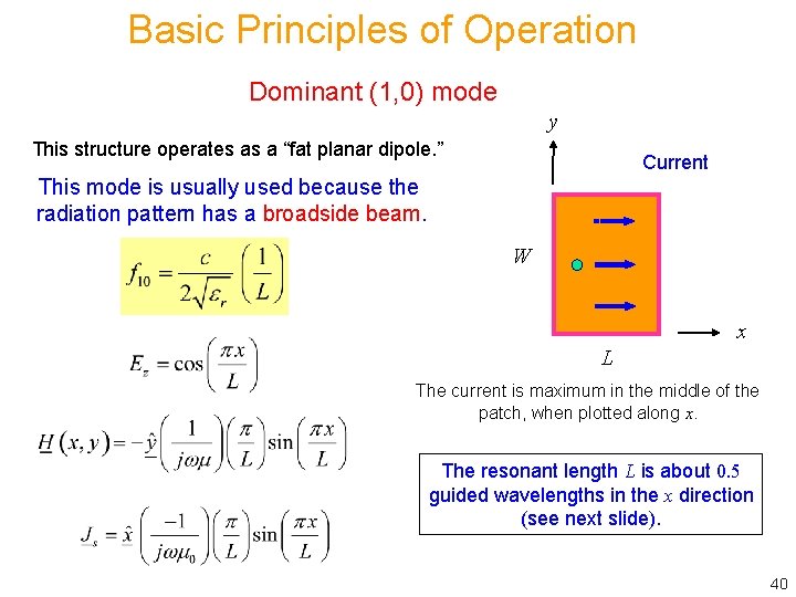
Basic Principles of Operation Dominant (1, 0) mode y This structure operates as a “fat planar dipole. ” Current This mode is usually used because the radiation pattern has a broadside beam. W x L The current is maximum in the middle of the patch, when plotted along x. The resonant length L is about 0. 5 guided wavelengths in the x direction (see next slide). 40

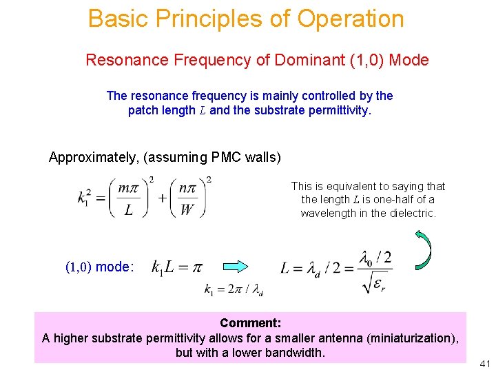
Basic Principles of Operation Resonance Frequency of Dominant (1, 0) Mode The resonance frequency is mainly controlled by the patch length L and the substrate permittivity. Approximately, (assuming PMC walls) This is equivalent to saying that the length L is one-half of a wavelength in the dielectric. (1, 0) mode: Comment: A higher substrate permittivity allows for a smaller antenna (miniaturization), but with a lower bandwidth. 41

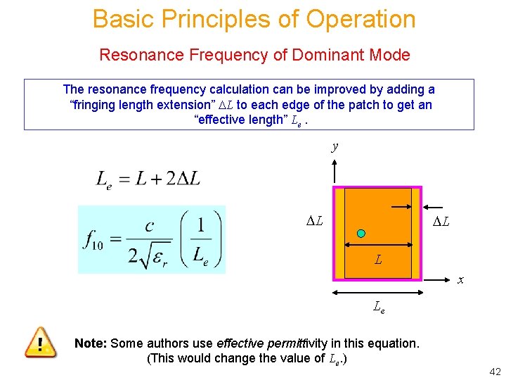
Basic Principles of Operation Resonance Frequency of Dominant Mode The resonance frequency calculation can be improved by adding a “fringing length extension” L to each edge of the patch to get an “effective length” Le. y L L L x Le Note: Some authors use effective permittivity in this equation. (This would change the value of Le. ) 42

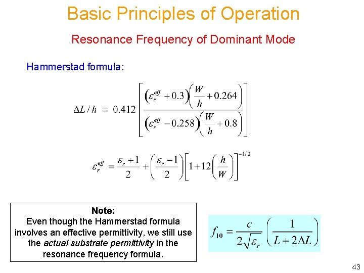
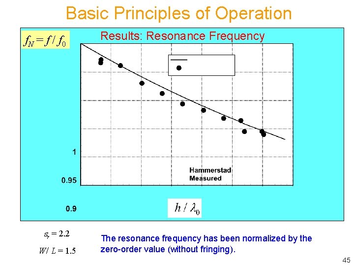
Basic Principles of Operation Resonance Frequency of Dominant Mode Hammerstad formula: Note: Even though the Hammerstad formula involves an effective permittivity, we still use the actual substrate permittivity in the resonance frequency formula. 43

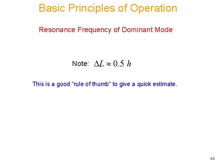
Basic Principles of Operation Resonance Frequency of Dominant Mode Note: This is a good “rule of thumb” to give a quick estimate. 44

Basic Principles of Operation f. N = f / f 0 r = 2. 2 W/ L = 1. 5 Results: Resonance Frequency The resonance frequency has been normalized by the zero-order value (without fringing). 45

Outline v Overview of microstrip antennas v Feeding methods v Basic principles of operation v General characteristics v CAD Formulas v Input Impedance v Radiation pattern v Circular polarization v Circular patch v Improving bandwidth v Miniaturization v Reducing surface waves and lateral radiation 46

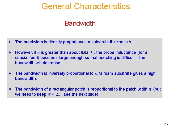
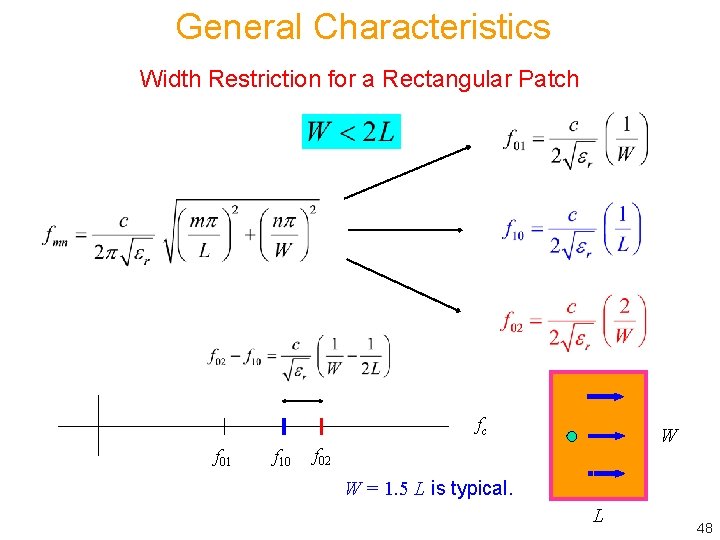
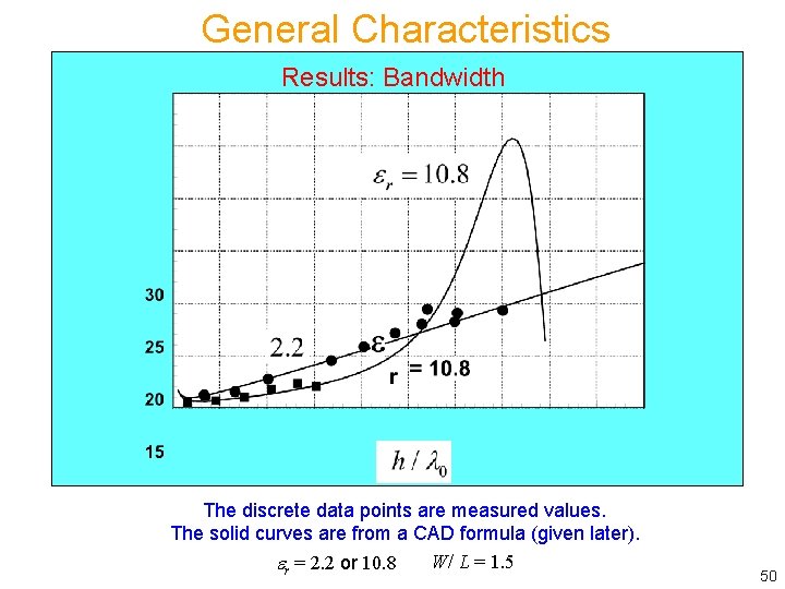
General Characteristics Bandwidth Ø The bandwidth is directly proportional to substrate thickness h. Ø However, if h is greater than about 0. 05 0 , the probe inductance (for a coaxial feed) becomes large enough so that matching is difficult – the bandwidth will decrease. Ø The bandwidth is inversely proportional to r (a foam substrate gives a high bandwidth). Ø The bandwidth of a rectangular patch is proportional to the patch width W (but we need to keep W < 2 L ; see the next slide). 47

General Characteristics Width Restriction for a Rectangular Patch fc f 01 f 10 W f 02 W = 1. 5 L is typical. L 48

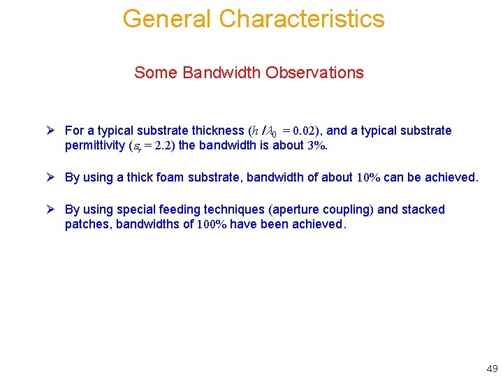
General Characteristics Some Bandwidth Observations Ø For a typical substrate thickness (h / 0 = 0. 02), and a typical substrate permittivity ( r = 2. 2) the bandwidth is about 3%. Ø By using a thick foam substrate, bandwidth of about 10% can be achieved. Ø By using special feeding techniques (aperture coupling) and stacked patches, bandwidths of 100% have been achieved. 49

General Characteristics Results: Bandwidth The discrete data points are measured values. The solid curves are from a CAD formula (given later). W/ L = 1. 5 r = 2. 2 or 10. 8 50

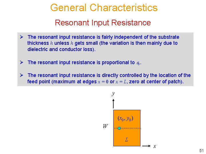
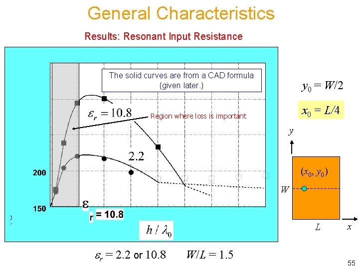
General Characteristics Resonant Input Resistance Ø The resonant input resistance is fairly independent of the substrate thickness h unless h gets small (the variation is then mainly due to dielectric and conductor loss). Ø The resonant input resistance is proportional to r. Ø The resonant input resistance is directly controlled by the location of the feed point (maximum at edges x = 0 or x = L, zero at center of patch). y (x 0, y 0) W L L x 51

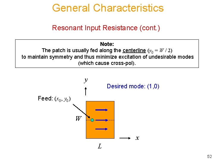
General Characteristics Resonant Input Resistance (cont. ) Note: The patch is usually fed along the centerline (y 0 = W / 2) to maintain symmetry and thus minimize excitation of undesirable modes (which cause cross-pol). y Desired mode: (1, 0) Feed: (x 0, y 0) W x L 52

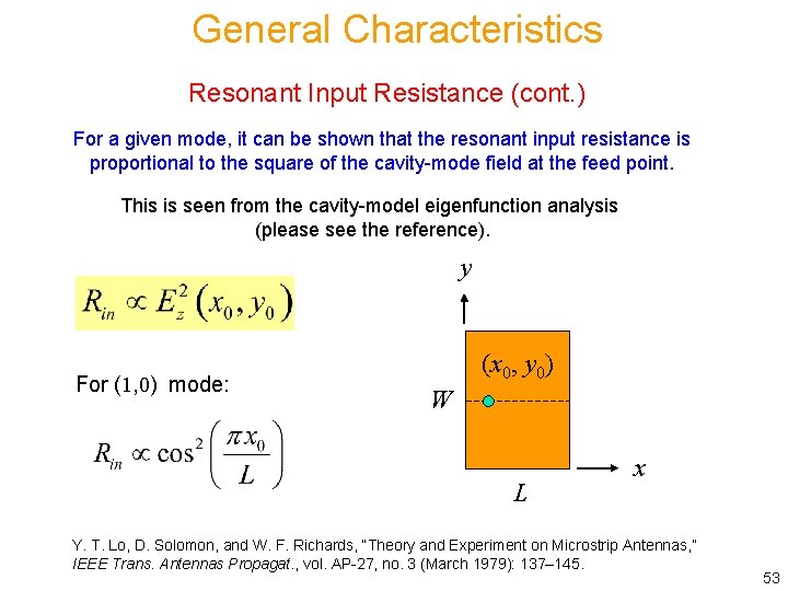
General Characteristics Resonant Input Resistance (cont. ) For a given mode, it can be shown that the resonant input resistance is proportional to the square of the cavity-mode field at the feed point. This is seen from the cavity-model eigenfunction analysis (please see the reference). y For (1, 0) mode: (x 0, y 0) W L x Y. T. Lo, D. Solomon, and W. F. Richards, “Theory and Experiment on Microstrip Antennas, ” IEEE Trans. Antennas Propagat. , vol. AP-27, no. 3 (March 1979): 137– 145. 53

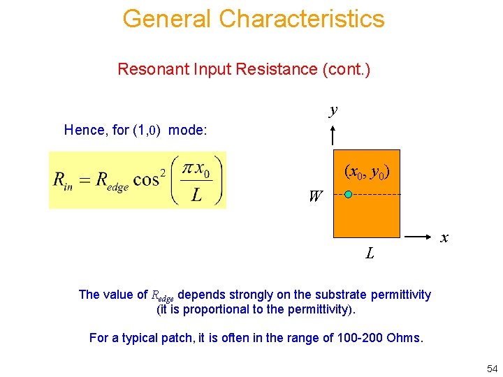
General Characteristics Resonant Input Resistance (cont. ) y Hence, for (1, 0) mode: (x 0, y 0) W L x The value of Redge depends strongly on the substrate permittivity (it is proportional to the permittivity). For a typical patch, it is often in the range of 100 -200 Ohms. 54

General Characteristics Results: Resonant Input Resistance The solid curves are from a CAD formula (given later. ) y 0 = W/2 x 0 = L/4 Region where loss is important y (x 0, y 0) W L r = 2. 2 or 10. 8 W/L = 1. 5 x 55

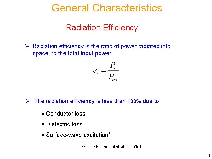
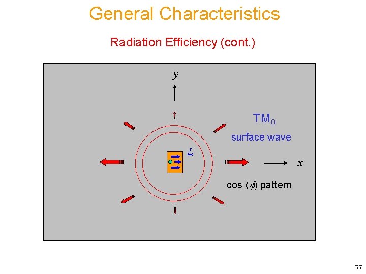
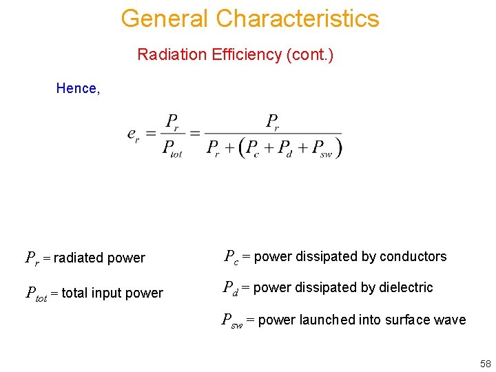
General Characteristics Radiation Efficiency Ø Radiation efficiency is the ratio of power radiated into space, to the total input power. Ø The radiation efficiency is less than 100% due to § Conductor loss § Dielectric loss § Surface-wave excitation* *assuming the substrate is infinite 56

General Characteristics Radiation Efficiency (cont. ) y TM 0 surface wave Js x cos ( ) pattern 57

General Characteristics Radiation Efficiency (cont. ) Hence, Pr = radiated power Pc = power dissipated by conductors Ptot = total input power Pd = power dissipated by dielectric Psw = power launched into surface wave 58

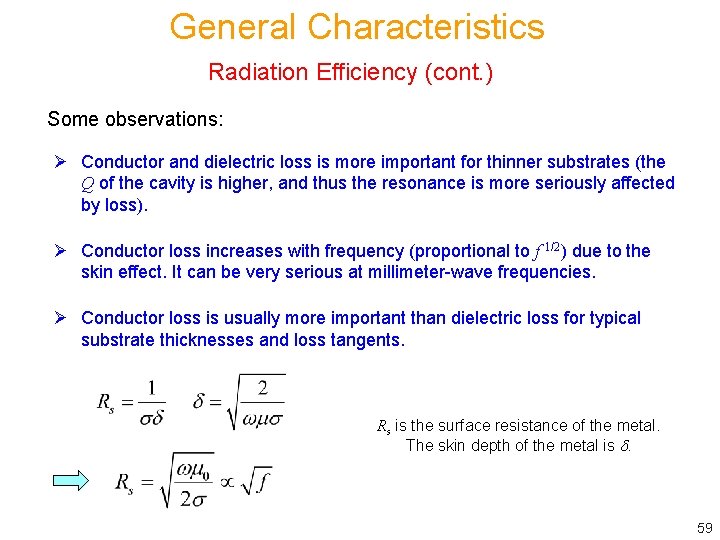
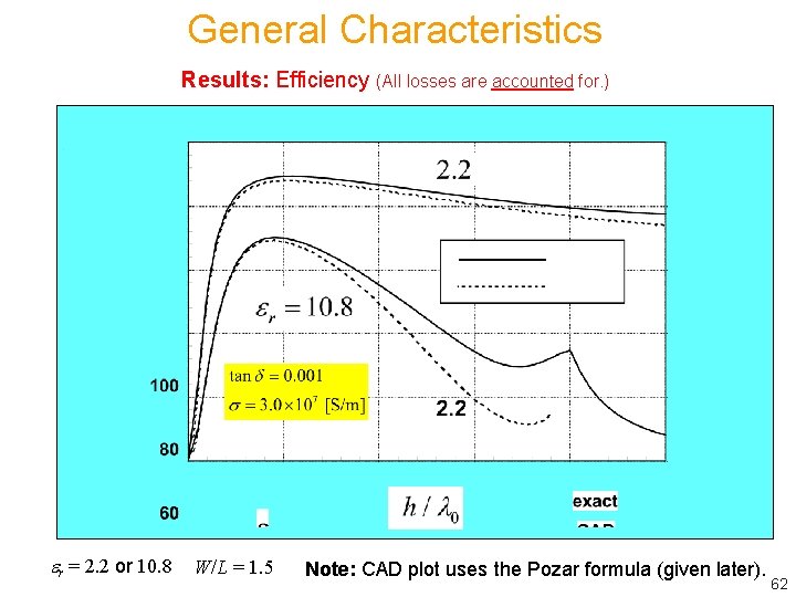
General Characteristics Radiation Efficiency (cont. ) Some observations: Ø Conductor and dielectric loss is more important for thinner substrates (the Q of the cavity is higher, and thus the resonance is more seriously affected by loss). Ø Conductor loss increases with frequency (proportional to f 1/2) due to the skin effect. It can be very serious at millimeter-wave frequencies. Ø Conductor loss is usually more important than dielectric loss for typical substrate thicknesses and loss tangents. Rs is the surface resistance of the metal. The skin depth of the metal is . 59

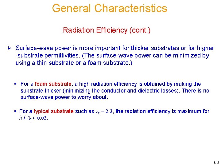
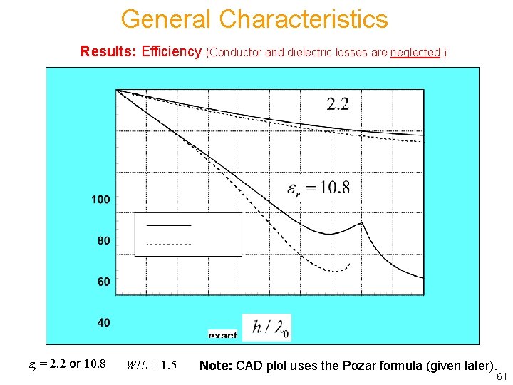
General Characteristics Radiation Efficiency (cont. ) Ø Surface-wave power is more important for thicker substrates or for higher -substrate permittivities. (The surface-wave power can be minimized by using a thin substrate or a foam substrate. ) § For a foam substrate, a high radiation efficiency is obtained by making the substrate thicker (minimizing the conductor and dielectric losses). There is no surface-wave power to worry about. § For a typical substrate such as r = 2. 2, the radiation efficiency is maximum for h / 0 0. 02. 60

General Characteristics Results: Efficiency (Conductor and dielectric losses are neglected. ) 2. 2 10. 8 r = 2. 2 or 10. 8 W/L = 1. 5 Note: CAD plot uses the Pozar formula (given later). 61

General Characteristics Results: Efficiency (All losses are accounted for. ) r = 2. 2 or 10. 8 W/L = 1. 5 Note: CAD plot uses the Pozar formula (given later). 62

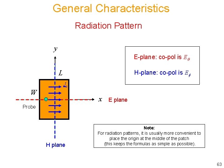
General Characteristics Radiation Pattern y E-plane: co-pol is E L H-plane: co-pol is E Js W x E plane Probe H plane Note: For radiation patterns, it is usually more convenient to place the origin at the middle of the patch (this keeps the formulas as simple as possible). 63

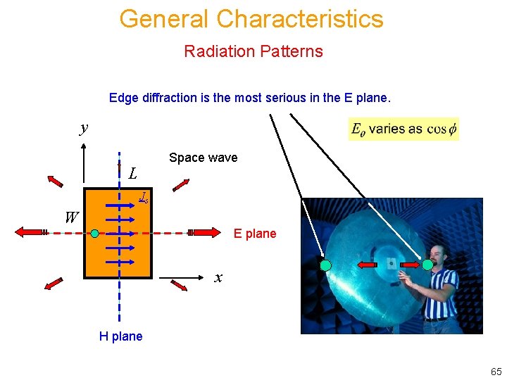
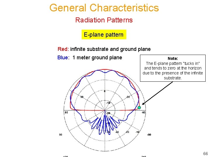
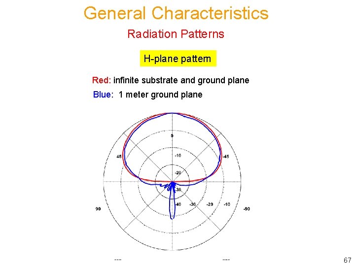
General Characteristics Radiation Patterns (cont. ) Comments on radiation patterns: Ø The E-plane pattern is typically broader than the H-plane pattern. Ø The truncation of the ground plane will cause edge diffraction, which tends to degrade the pattern by introducing: § Rippling in the forward direction § Back-radiation Ø Pattern distortion is more severe in the E-plane, due to the angle dependence of the vertical polarization E on the ground plane. (It varies as cos ( )). 64

General Characteristics Radiation Patterns Edge diffraction is the most serious in the E plane. y Space wave L Js W E plane x H plane 65

General Characteristics Radiation Patterns E-plane pattern Red: infinite substrate and ground plane Blue: 1 meter ground plane Note: The E-plane pattern “tucks in” and tends to zero at the horizon due to the presence of the infinite substrate. 66

General Characteristics Radiation Patterns H-plane pattern Red: infinite substrate and ground plane Blue: 1 meter ground plane 67

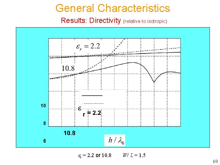
General Characteristics Directivity Ø The directivity is fairly insensitive to the substrate thickness. Ø The directivity is higher for lower permittivity, because the patch is larger. 68

General Characteristics Results: Directivity (relative to isotropic) r = 2. 2 or 10. 8 W/ L = 1. 5 69

Outline v Overview of microstrip antennas v Feeding methods v Basic principles of operation v General characteristics v CAD Formulas v Input Impedance v Radiation pattern v Circular polarization v Circular patch v Improving bandwidth v Miniaturization v Reducing surface waves and lateral radiation 70

CAD Formulas CAD formulas for the important properties of the rectangular microstrip antenna will be shown. Ø Radiation efficiency Ø Bandwidth (Q) Ø Resonant input resistance Ø Directivity § D. R. Jackson, “Microstrip Antennas, ” Chapter 7 of Antenna Engineering Handbook, 5 th Ed. , J. L. Volakis, Editor, Mc. Graw Hill, 2019. § D. R. Jackson, S. A. Long, J. T. Williams, and V. B. Davis, “Computer-Aided Design of Rectangular Microstrip Antennas, ” Ch. 5 of Advances in Microstrip and Printed Antennas, K. F. Lee and W. Chen, Eds. , John Wiley, 1997. § D. R. Jackson and N. G. Alexopoulos, “Simple Approximate Formulas for Input Resistance, Bandwidth, and Efficiency of a Resonant Rectangular Patch, ” IEEE Trans. Antennas and Propagation, Vol. 39, pp. 407 -410, March 1991. 71

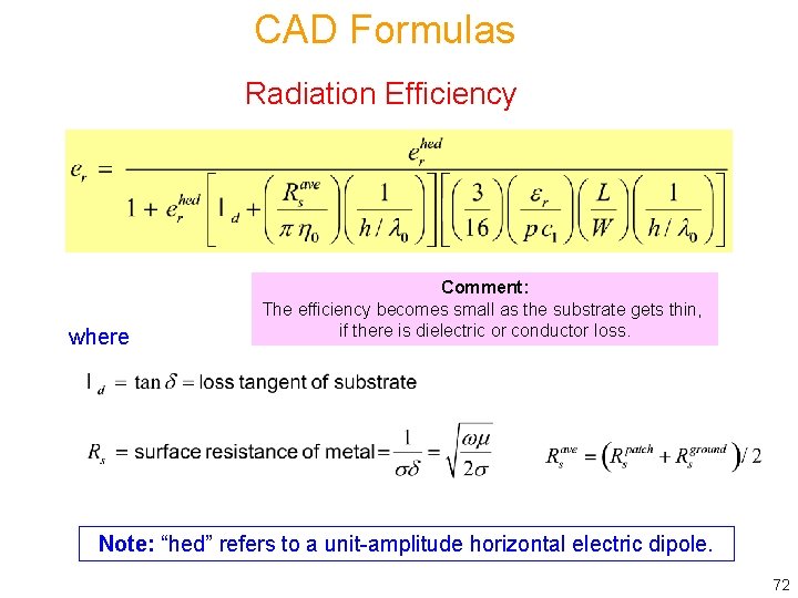
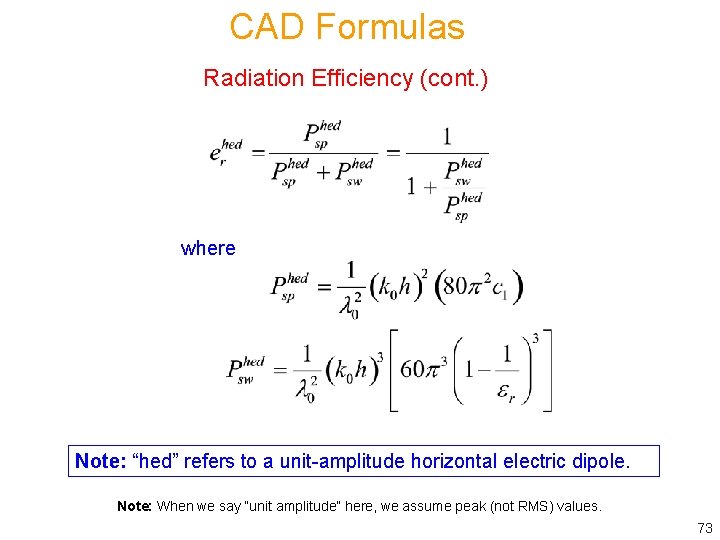
CAD Formulas Radiation Efficiency where Comment: The efficiency becomes small as the substrate gets thin, if there is dielectric or conductor loss. Note: “hed” refers to a unit-amplitude horizontal electric dipole. 72

CAD Formulas Radiation Efficiency (cont. ) where Note: “hed” refers to a unit-amplitude horizontal electric dipole. Note: When we say “unit amplitude” here, we assume peak (not RMS) values. 73

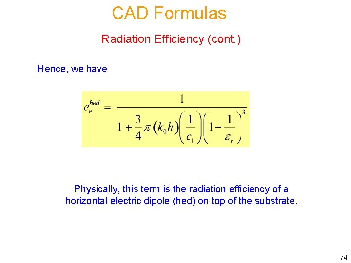
CAD Formulas Radiation Efficiency (cont. ) Hence, we have Physically, this term is the radiation efficiency of a horizontal electric dipole (hed) on top of the substrate. 74

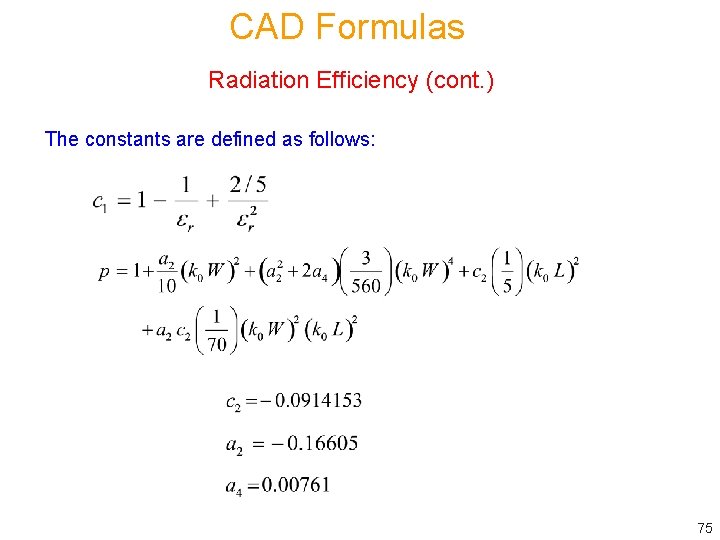
CAD Formulas Radiation Efficiency (cont. ) The constants are defined as follows: 75

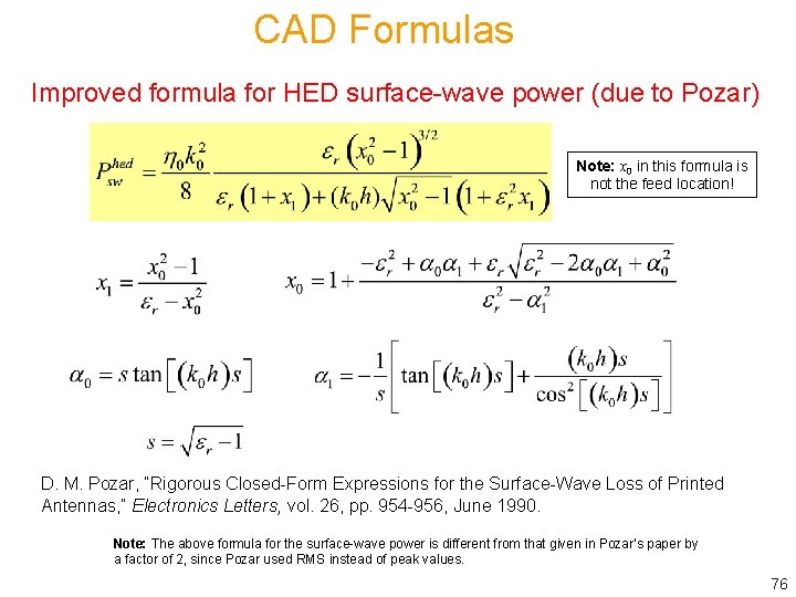
CAD Formulas Improved formula for HED surface-wave power (due to Pozar) Note: x 0 in this formula is not the feed location! D. M. Pozar, “Rigorous Closed-Form Expressions for the Surface-Wave Loss of Printed Antennas, ” Electronics Letters, vol. 26, pp. 954 -956, June 1990. Note: The above formula for the surface-wave power is different from that given in Pozar’s paper by a factor of 2, since Pozar used RMS instead of peak values. 76

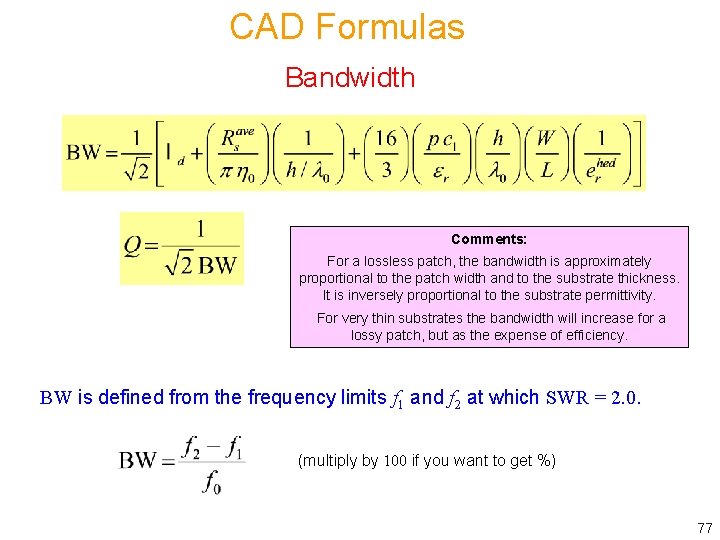
CAD Formulas Bandwidth Comments: For a lossless patch, the bandwidth is approximately proportional to the patch width and to the substrate thickness. It is inversely proportional to the substrate permittivity. For very thin substrates the bandwidth will increase for a lossy patch, but as the expense of efficiency. BW is defined from the frequency limits f 1 and f 2 at which SWR = 2. 0. (multiply by 100 if you want to get %) 77

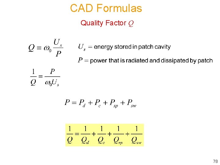
CAD Formulas Quality Factor Q 78

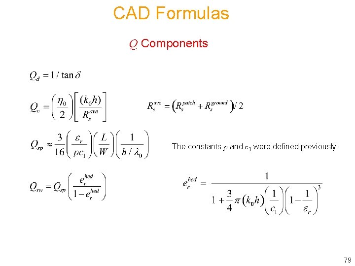
CAD Formulas Q Components The constants p and c 1 were defined previously. 79

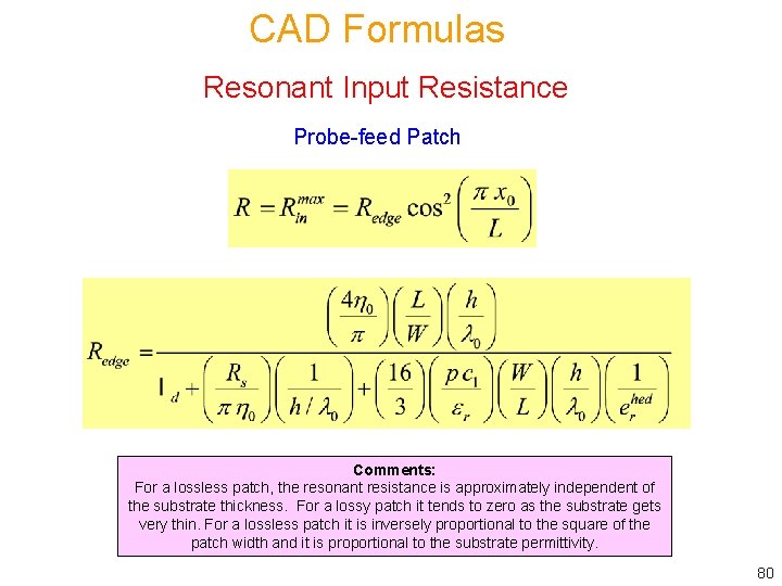
CAD Formulas Resonant Input Resistance Probe-feed Patch Comments: For a lossless patch, the resonant resistance is approximately independent of the substrate thickness. For a lossy patch it tends to zero as the substrate gets very thin. For a lossless patch it is inversely proportional to the square of the patch width and it is proportional to the substrate permittivity. 80

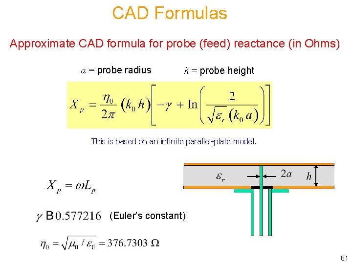
CAD Formulas Approximate CAD formula for probe (feed) reactance (in Ohms) a = probe radius h = probe height This is based on an infinite parallel-plate model. (Euler’s constant) 81

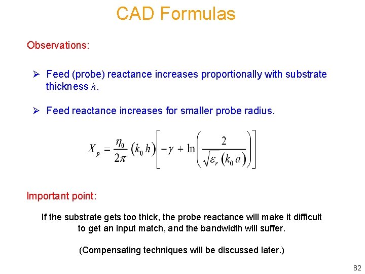
CAD Formulas Observations: Ø Feed (probe) reactance increases proportionally with substrate thickness h. Ø Feed reactance increases for smaller probe radius. Important point: If the substrate gets too thick, the probe reactance will make it difficult to get an input match, and the bandwidth will suffer. (Compensating techniques will be discussed later. ) 82

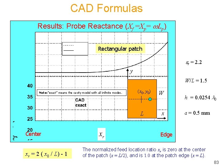
CAD Formulas Results: Probe Reactance (Xf =Xp= Lp) Rectangular patch r = 2. 2 y W/L = 1. 5 (x 0, y 0) Note: “exact” means the cavity model with all infinite modes. L Center xr = 2 ( x 0 / L) - 1 L W x h = 0. 0254 0 a = 0. 5 mm Edge The normalized feed location ratio xr is zero at the center of the patch (x = L/2), and is 1. 0 at the patch edge (x = L). 83

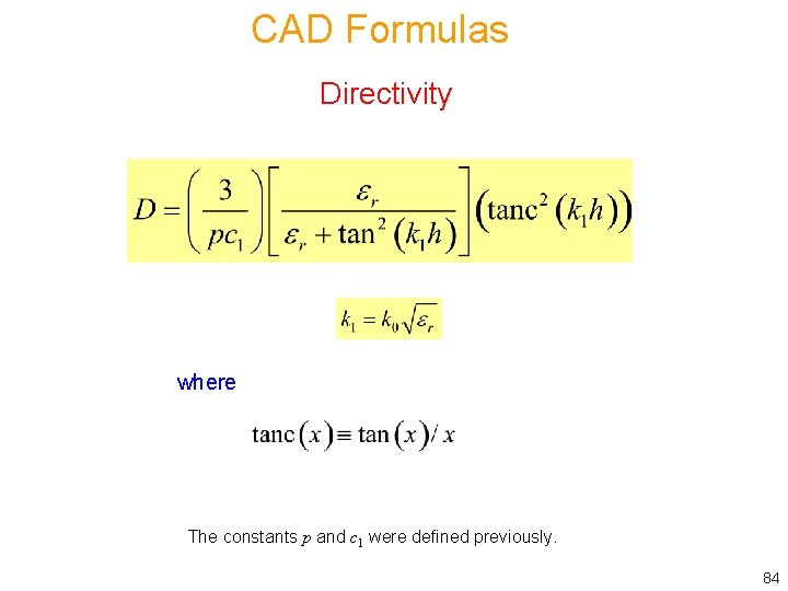
CAD Formulas Directivity where The constants p and c 1 were defined previously. 84

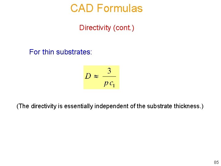
CAD Formulas Directivity (cont. ) For thin substrates: (The directivity is essentially independent of the substrate thickness. ) 85

Outline v Overview of microstrip antennas v Feeding methods v Basic principles of operation v General characteristics v CAD Formulas v Input Impedance v Radiation pattern v Circular polarization v Circular patch v Improving bandwidth v Miniaturization v Reducing surface waves and lateral radiation 86

Input Impedance Various models have been proposed over the years for calculating the input impedance of a microstrip patch antenna. § Transmission line model Ø The first model introduced Ø Very simple § Cavity model (eigenfunction expansion) Ø Simple yet accurate for thin substrates Ø Gives physical insight into operation § CAD circuit model Ø Extremely simple and almost as accurate as the cavity model § Spectral-domain method Ø More challenging to implement Ø Accounts rigorously for both radiation and surface-wave excitation § Commercial software Ø Very accurate Ø Can be time consuming 87

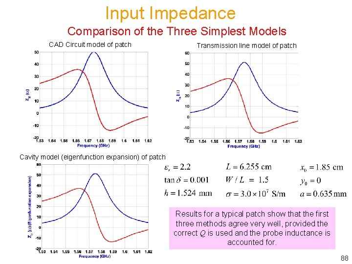
Input Impedance Comparison of the Three Simplest Models CAD Circuit model of patch Transmission line model of patch Cavity model (eigenfunction expansion) of patch Results for a typical patch show that the first three methods agree very well, provided the correct Q is used and the probe inductance is accounted for. 88

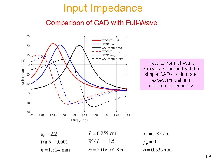
Input Impedance Comparison of CAD with Full-Wave Results from full-wave analysis agree well with the simple CAD circuit model, except for a shift in resonance frequency. 89

Input Impedance CAD Circuit Model for Input Impedance The circuit model discussed assumes a probe feed. Other circuit models exist for other types of feeds. Note: The mathematical justification of the CAD circuit model comes from a cavity-model eigenfunction analysis. Y. T. Lo, D. Solomon, and W. F. Richards, “Theory and Experiment on Microstrip Antennas, ” IEEE Trans. Antennas Propagat. , vol. AP-27, no. 3 (March 1979): 137– 145. 90

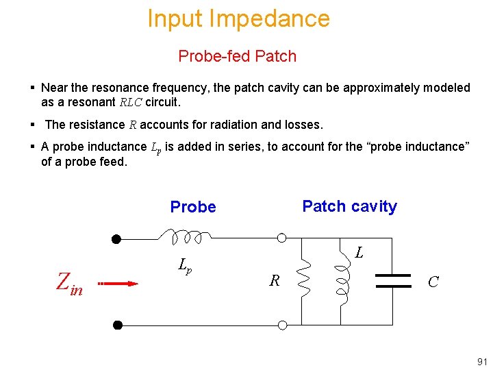
Input Impedance Probe-fed Patch § Near the resonance frequency, the patch cavity can be approximately modeled as a resonant RLC circuit. § The resistance R accounts for radiation and losses. § A probe inductance Lp is added in series, to account for the “probe inductance” of a probe feed. Patch cavity Probe Zin Lp L R C 91

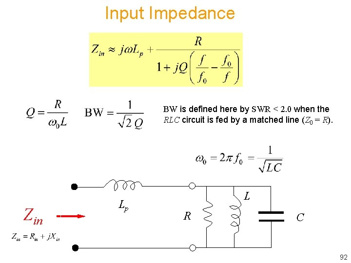
Input Impedance BW is defined here by SWR < 2. 0 when the RLC circuit is fed by a matched line (Z 0 = R). Zin Lp L R C 92

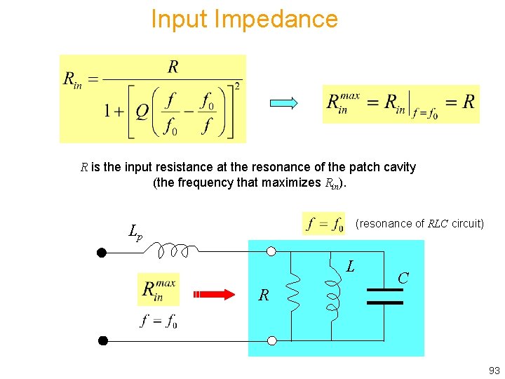
Input Impedance R is the input resistance at the resonance of the patch cavity (the frequency that maximizes Rin). (resonance of RLC circuit) Lp L R C 93

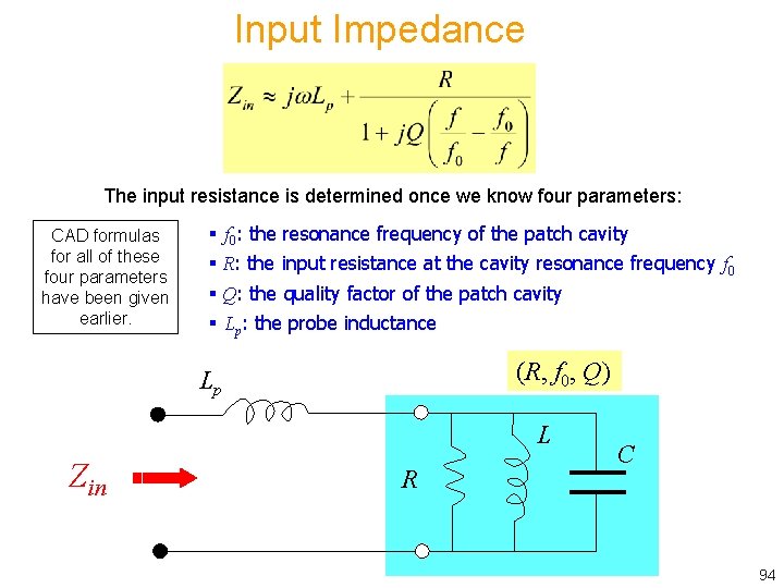
Input Impedance The input resistance is determined once we know four parameters: CAD formulas for all of these four parameters have been given earlier. § f 0: the resonance frequency of the patch cavity § R: the input resistance at the cavity resonance frequency f 0 § Q: the quality factor of the patch cavity § Lp: the probe inductance (R, f 0, Q) Lp L Zin R C 94

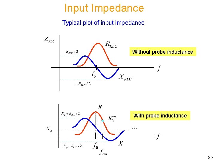
Input Impedance Typical plot of input impedance Without probe inductance With probe inductance 95

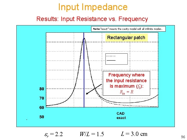
Input Impedance Results: Input Resistance vs. Frequency Note: “exact” means the cavity model will all infinite modes. Rectangular patch Frequency where the input resistance is maximum (f 0): Rin = R r = 2. 2 W/L = 1. 5 L = 3. 0 cm 96

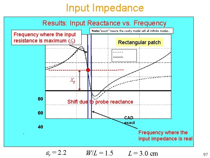
Input Impedance Results: Input Reactance vs. Frequency where the input resistance is maximum (f 0) Note: “exact” means the cavity model will all infinite modes. Rectangular patch Xp Shift due to probe reactance Frequency where the input impedance is real r = 2. 2 W/L = 1. 5 L = 3. 0 cm 97

Input Impedance Optimization to get exactly 50 at the desired resonance frequency: Ø Vary the length L first until you find the value that gives an input reactance of zero at the desired frequency. Ø Then adjust the feed position x 0 to make the real part of the input impedance 50 at this frequency. 98

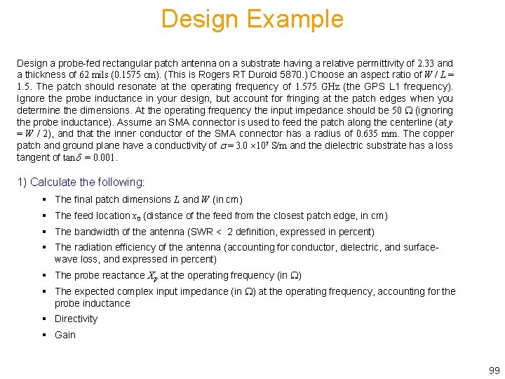
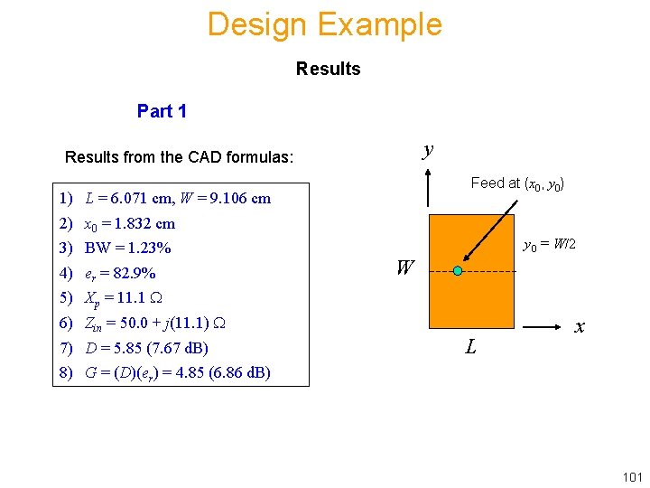
Design Example Design a probe-fed rectangular patch antenna on a substrate having a relative permittivity of 2. 33 and a thickness of 62 mils (0. 1575 cm). (This is Rogers RT Duroid 5870. ) Choose an aspect ratio of W / L = 1. 5. The patch should resonate at the operating frequency of 1. 575 GHz (the GPS L 1 frequency). Ignore the probe inductance in your design, but account for fringing at the patch edges when you determine the dimensions. At the operating frequency the input impedance should be 50 (ignoring the probe inductance). Assume an SMA connector is used to feed the patch along the centerline (at y = W / 2), and that the inner conductor of the SMA connector has a radius of 0. 635 mm. The copper patch and ground plane have a conductivity of = 3. 0 107 S/m and the dielectric substrate has a loss tangent of tan = 0. 001. 1) Calculate the following: § The final patch dimensions L and W (in cm) § The feed location x 0 (distance of the feed from the closest patch edge, in cm) § The bandwidth of the antenna (SWR < 2 definition, expressed in percent) § The radiation efficiency of the antenna (accounting for conductor, dielectric, and surfacewave loss, and expressed in percent) § The probe reactance Xp at the operating frequency (in ) § The expected complex input impedance (in ) at the operating frequency, accounting for the probe inductance § Directivity § Gain 99

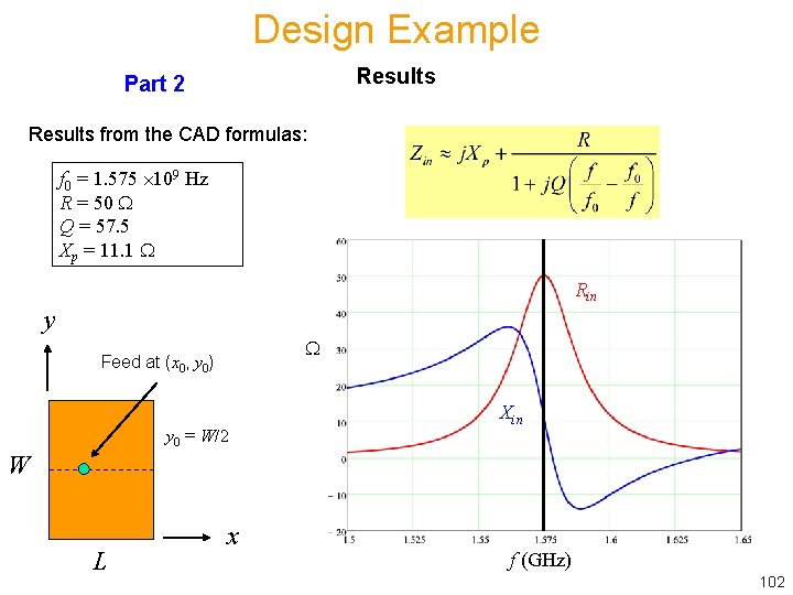
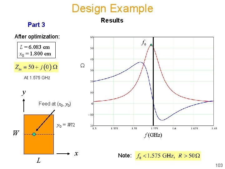
Design Example Continued 2) Find (f 0, R, Xp, and Q) and plot the input impedance vs. frequency using the CAD circuit model. 3) Keep W/L = 1. 5, but now vary the length L of the patch and the feed position x 0 until you find the value that makes the input impedance exactly 50+j(0) at 1. 575 GHz. 100

Design Example Results Part 1 y Results from the CAD formulas: Feed at (x 0, y 0) 1) L = 6. 071 cm, W = 9. 106 cm 2) x 0 = 1. 832 cm 3) BW = 1. 23% 4) er = 82. 9% y 0 = W/2 W 5) Xp = 11. 1 6) Zin = 50. 0 + j(11. 1) 7) D = 5. 85 (7. 67 d. B) L x 8) G = (D)(er) = 4. 85 (6. 86 d. B) 101

Design Example Results Part 2 Results from the CAD formulas: f 0 = 1. 575 109 Hz R = 50 Q = 57. 5 Xp = 11. 1 Rin y Feed at (x 0, y 0) y 0 = W/2 Xin W L x f (GHz) 102

Design Example Results Part 3 After optimization: L = 6. 083 cm x 0 = 1. 800 cm At 1. 575 GHz y Feed at (x 0, y 0) y 0 = W/2 W f (GHz) L x Note: 103

Outline v Overview of microstrip antennas v Feeding methods v Basic principles of operation v General characteristics v CAD Formulas v Input Impedance v Radiation pattern v Circular polarization v Circular patch v Improving bandwidth v Miniaturization v Reducing surface waves and lateral radiation 104

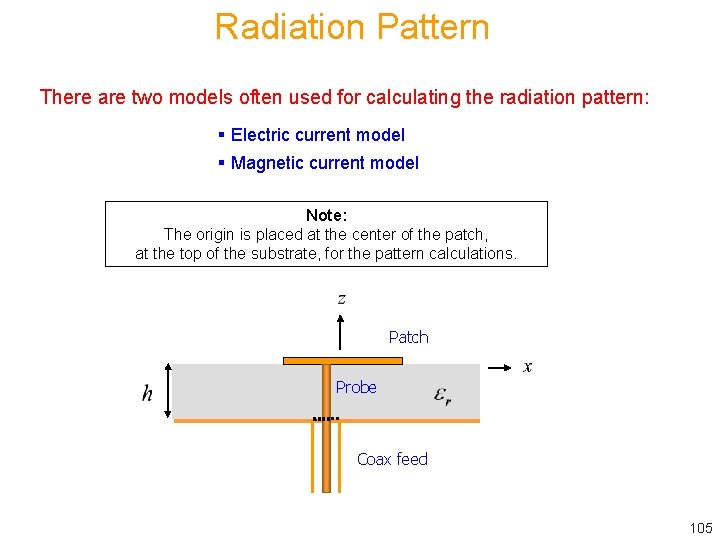
Radiation Pattern There are two models often used for calculating the radiation pattern: § Electric current model § Magnetic current model Note: The origin is placed at the center of the patch, at the top of the substrate, for the pattern calculations. Patch Probe Coax feed 105

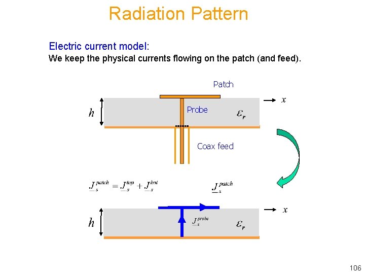
Radiation Pattern Electric current model: We keep the physical currents flowing on the patch (and feed). Patch Probe Coax feed 106

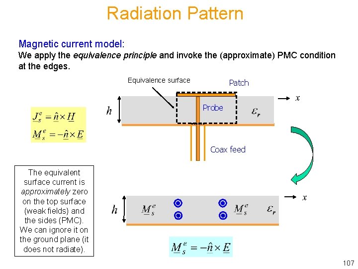
Radiation Pattern Magnetic current model: We apply the equivalence principle and invoke the (approximate) PMC condition at the edges. Equivalence surface Patch Probe Coax feed The equivalent surface current is approximately zero on the top surface (weak fields) and the sides (PMC). We can ignore it on the ground plane (it does not radiate). 107

Radiation Pattern Theorem The electric and magnetic models yield identical patterns at the resonance frequency of the cavity mode. Assumption: The electric and magnetic current models are based on the fields of a single cavity mode, corresponding to an ideal cavity with PMC walls. D. R. Jackson and J. T. Williams, “A Comparison of CAD Models for Radiation from Rectangular Microstrip Patches, ” Intl. Journal of Microwave and Millimeter-Wave Computer Aided Design, vol. 1, no. 2, pp. 236 -248, April 1991. 108

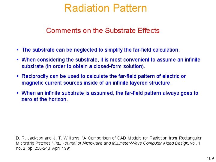
Radiation Pattern Comments on the Substrate Effects § The substrate can be neglected to simplify the far-field calculation. § When considering the substrate, it is most convenient to assume an infinite substrate (in order to obtain a closed-form solution). § Reciprocity can be used to calculate the far-field pattern of electric or magnetic current sources inside of an infinite layered structure. § When an infinite substrate is assumed, the far-field pattern always goes to zero at the horizon. D. R. Jackson and J. T. Williams, “A Comparison of CAD Models for Radiation from Rectangular Microstrip Patches, ” Intl. Journal of Microwave and Millimeter-Wave Computer Aided Design, vol. 1, no. 2, pp. 236 -248, April 1991. 109

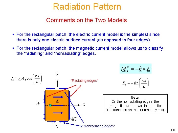
Radiation Pattern Comments on the Two Models § For the rectangular patch, the electric current model is the simplest since there is only one electric surface current (as opposed to four edges). § For the rectangular patch, the magnetic current model allows us to classify the “radiating” and “nonradiating” edges. y “Radiating edges” W x L Note: On the nonradiating edges, the magnetic currents are in opposite directions across the centerline (x = 0). “Nonradiating edges” 110

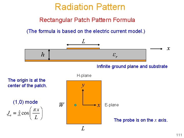
Radiation Pattern Rectangular Patch Pattern Formula (The formula is based on the electric current model. ) L x h Infinite ground plane and substrate H-plane The origin is at the center of the patch. (1, 0) mode y x W E-plane The probe is on the x axis. L 111

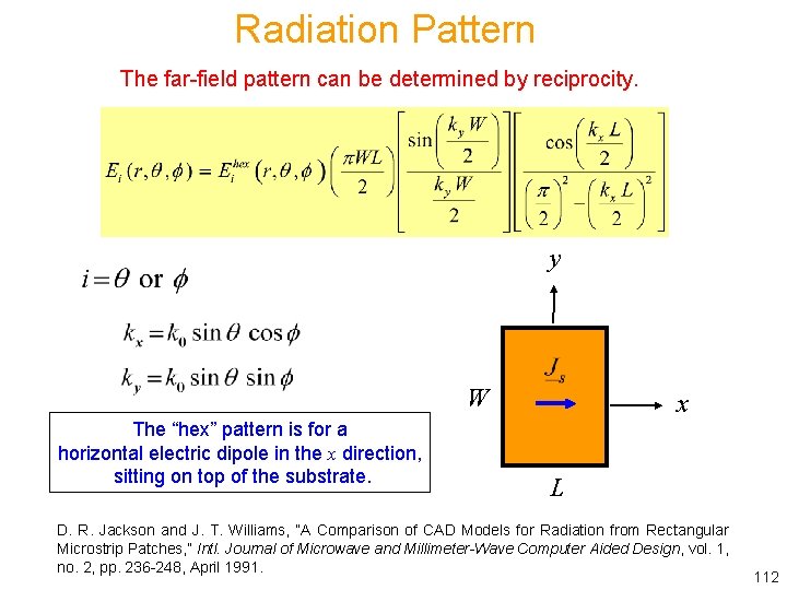
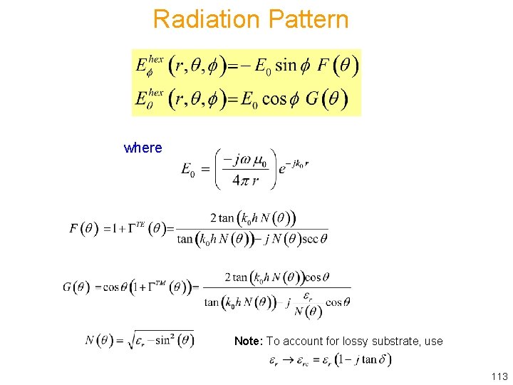
Radiation Pattern The far-field pattern can be determined by reciprocity. y W The “hex” pattern is for a horizontal electric dipole in the x direction, sitting on top of the substrate. x L D. R. Jackson and J. T. Williams, “A Comparison of CAD Models for Radiation from Rectangular Microstrip Patches, ” Intl. Journal of Microwave and Millimeter-Wave Computer Aided Design, vol. 1, no. 2, pp. 236 -248, April 1991. 112

Radiation Pattern where Note: To account for lossy substrate, use 113

Outline v Overview of microstrip antennas v Feeding methods v Basic principles of operation v General characteristics v CAD Formulas v Radiation pattern v Input Impedance v Circular polarization v Circular patch v Improving bandwidth v Miniaturization v Reducing surface waves and lateral radiation 114

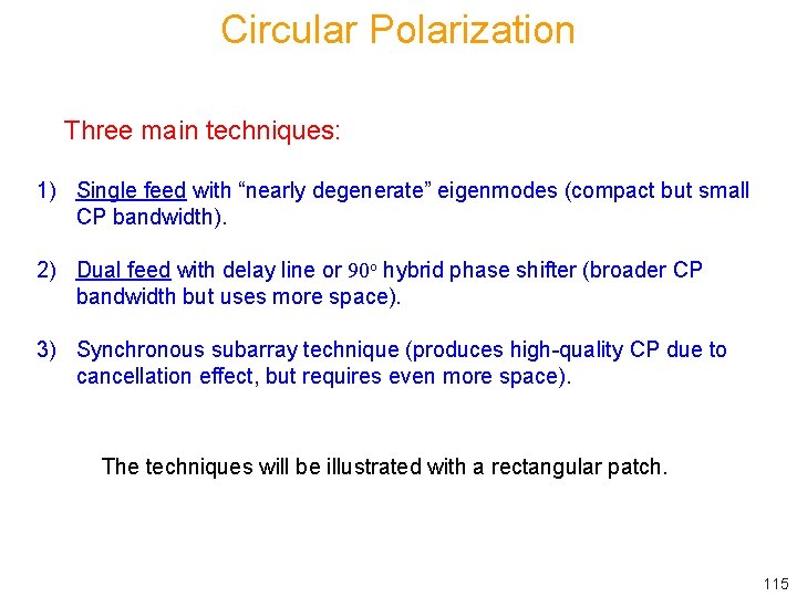
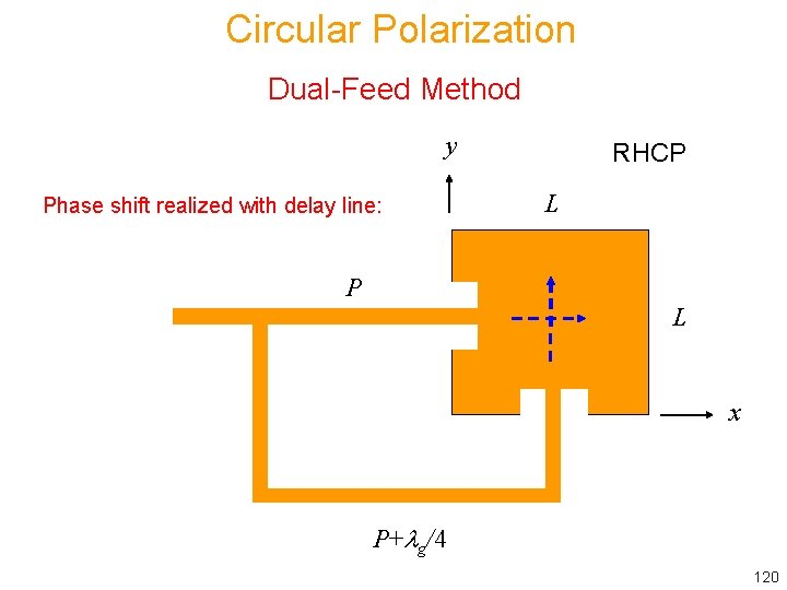
Circular Polarization Three main techniques: 1) Single feed with “nearly degenerate” eigenmodes (compact but small CP bandwidth). 2) Dual feed with delay line or 90 o hybrid phase shifter (broader CP bandwidth but uses more space). 3) Synchronous subarray technique (produces high-quality CP due to cancellation effect, but requires even more space). The techniques will be illustrated with a rectangular patch. 115

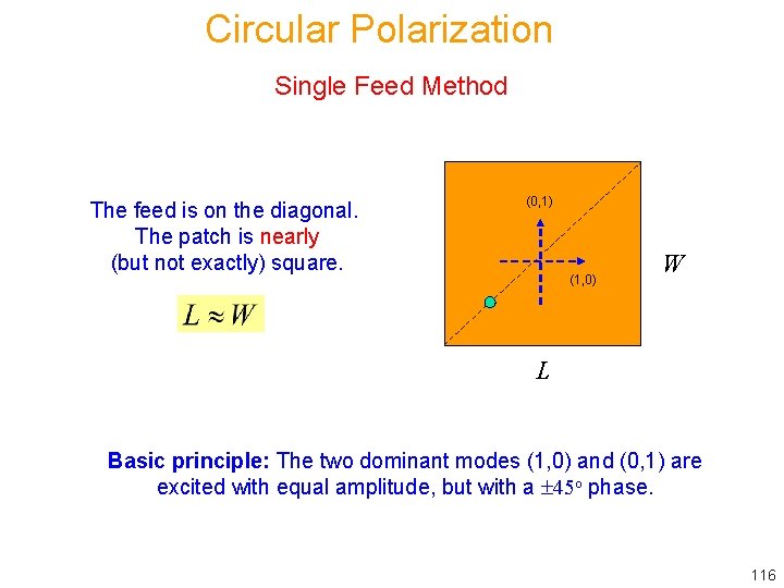
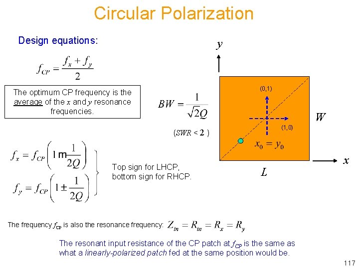
Circular Polarization Single Feed Method The feed is on the diagonal. The patch is nearly (but not exactly) square. (0, 1) (1, 0) W L Basic principle: The two dominant modes (1, 0) and (0, 1) are excited with equal amplitude, but with a 45 o phase. 116

Circular Polarization Design equations: y (0, 1) The optimum CP frequency is the average of the x and y resonance frequencies. W (1, 0) (SWR < 2 ) Top sign for LHCP, bottom sign for RHCP. L x The frequency f. CP is also the resonance frequency: The resonant input resistance of the CP patch at f. CP is the same as what a linearly-polarized patch fed at the same position would be. 117

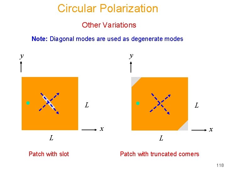
Circular Polarization Other Variations Note: Diagonal modes are used as degenerate modes y y L L x L Patch with slot x L Patch with truncated corners 118

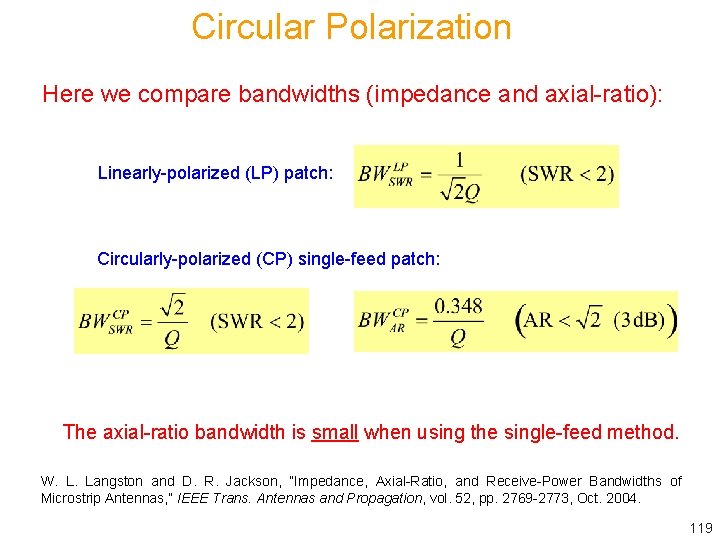
Circular Polarization Here we compare bandwidths (impedance and axial-ratio): Linearly-polarized (LP) patch: Circularly-polarized (CP) single-feed patch: The axial-ratio bandwidth is small when using the single-feed method. W. L. Langston and D. R. Jackson, “Impedance, Axial-Ratio, and Receive-Power Bandwidths of Microstrip Antennas, ” IEEE Trans. Antennas and Propagation, vol. 52, pp. 2769 -2773, Oct. 2004. 119

Circular Polarization Dual-Feed Method y Phase shift realized with delay line: RHCP L x P+ g/4 120

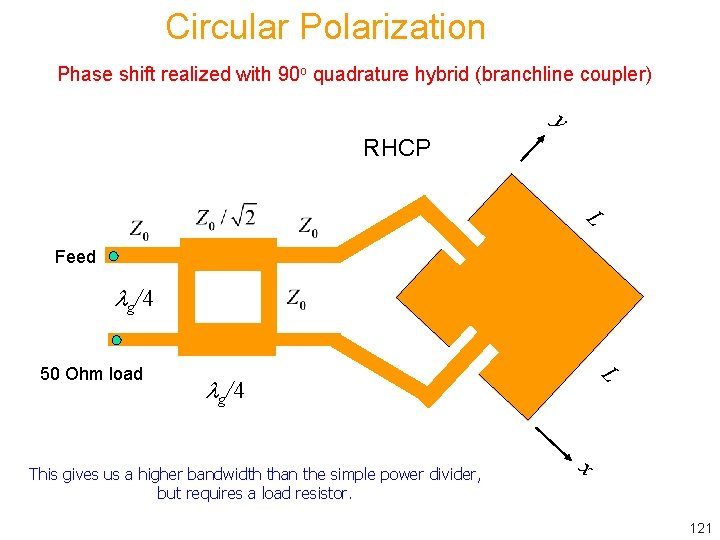
Circular Polarization Phase shift realized with 90 o quadrature hybrid (branchline coupler) y RHCP L Feed g/4 50 Ohm load L g/4 This gives us a higher bandwidth than the simple power divider, but requires a load resistor. x 121

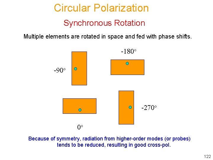
Circular Polarization Synchronous Rotation Multiple elements are rotated in space and fed with phase shifts. -180 o -90 o -270 o 0 o Because of symmetry, radiation from higher-order modes (or probes) tends to be reduced, resulting in good cross-pol. 122

Outline v Overview of microstrip antennas v Feeding methods v Basic principles of operation v General characteristics v CAD Formulas v Input Impedance v Radiation pattern v Circular polarization v Circular patch v Improving bandwidth v Miniaturization v Reducing surface waves and lateral radiation 123

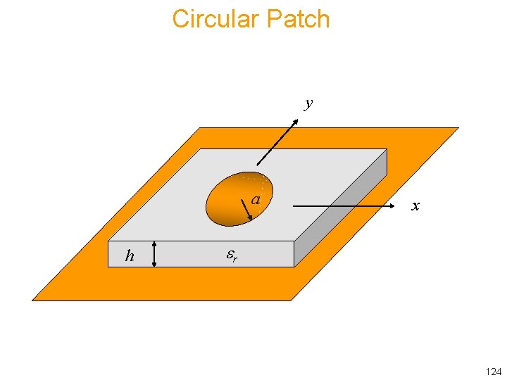
Circular Patch y a h x r 124

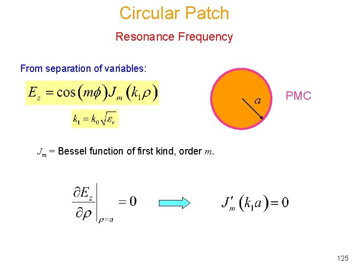
Circular Patch Resonance Frequency From separation of variables: a PMC Jm = Bessel function of first kind, order m. 125

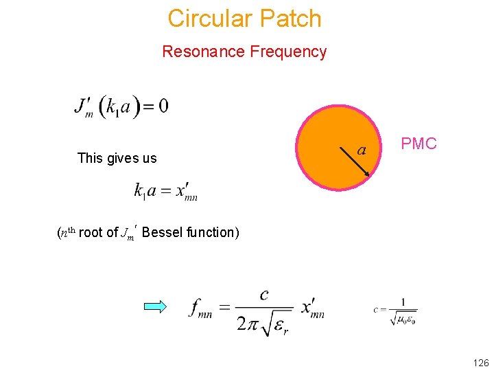
Circular Patch Resonance Frequency This gives us a PMC (nth root of Jm Bessel function) 126

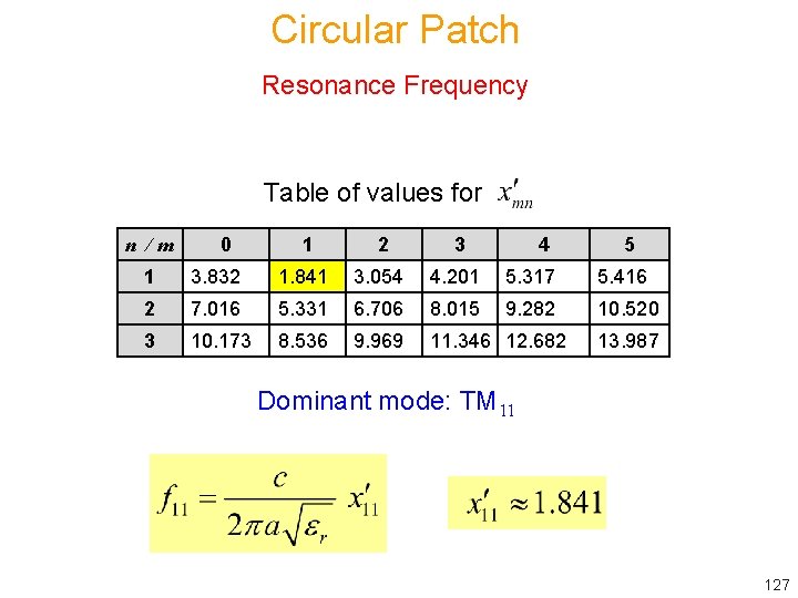
Circular Patch Resonance Frequency Table of values for n /m 0 1 2 3 4 5 1 3. 832 1. 841 3. 054 4. 201 5. 317 5. 416 2 7. 016 5. 331 6. 706 8. 015 9. 282 10. 520 3 10. 173 8. 536 9. 969 11. 346 12. 682 13. 987 Dominant mode: TM 11 127

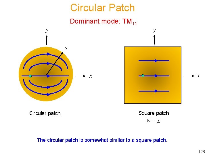
Circular Patch Dominant mode: TM 11 y y a x x Circular patch Square patch W=L The circular patch is somewhat similar to a square patch. 128

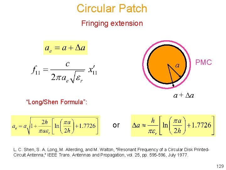
Circular Patch Fringing extension a PMC a + a “Long/Shen Formula”: or L. C. Shen, S. A. Long, M. Allerding, and M. Walton, "Resonant Frequency of a Circular Disk Printed. Circuit Antenna, " IEEE Trans. Antennas and Propagation, vol. 25, pp. 595 -596, July 1977. 129

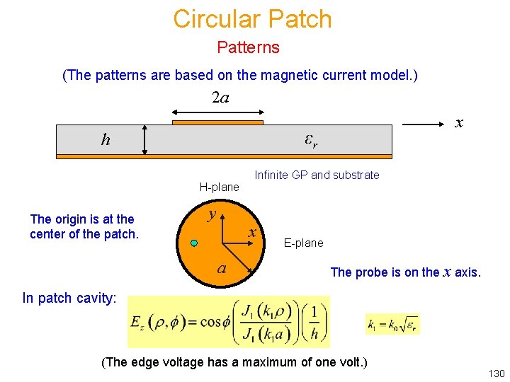
Circular Patch Patterns (The patterns are based on the magnetic current model. ) 2 a x h H-plane The origin is at the center of the patch. y Infinite GP and substrate x a E-plane The probe is on the x axis. In patch cavity: (The edge voltage has a maximum of one volt. ) 130

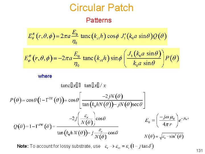
Circular Patch Patterns where Note: To account for lossy substrate, use 131

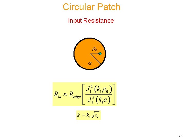
Circular Patch Input Resistance a 132

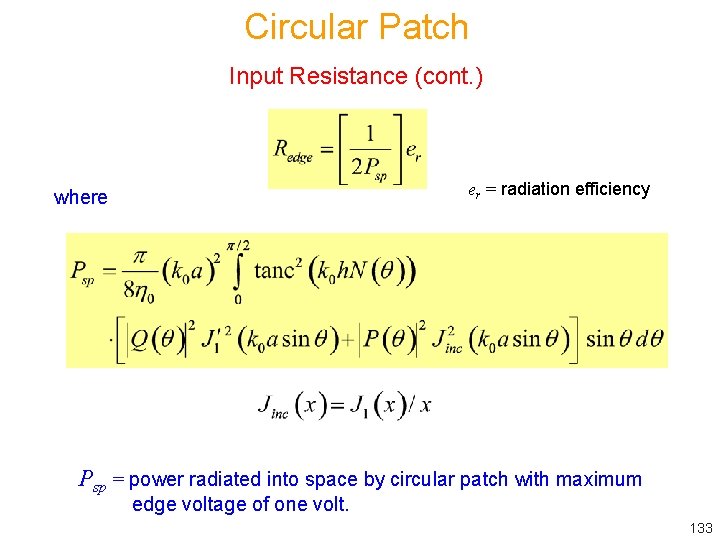
Circular Patch Input Resistance (cont. ) er = radiation efficiency where Psp = power radiated into space by circular patch with maximum edge voltage of one volt. 133

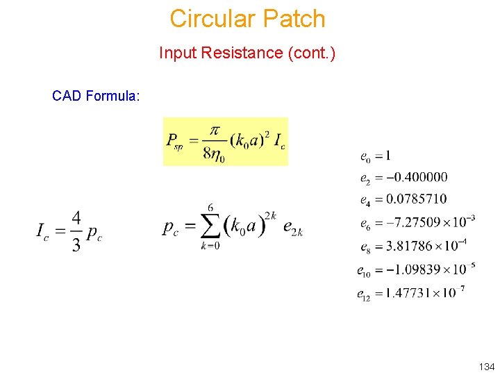
Circular Patch Input Resistance (cont. ) CAD Formula: 134

Outline v Overview of microstrip antennas v Feeding methods v Basic principles of operation v General characteristics v CAD Formulas v Input Impedance v Radiation pattern v Circular polarization v Circular patch v Improving bandwidth v Miniaturization v Reducing surface waves and lateral radiation 135

Improving Bandwidth Some of the techniques that have been successfully developed are illustrated here. The literature may be consulted for additional designs and variations. 136

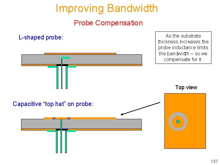
Improving Bandwidth Probe Compensation L-shaped probe: As the substrate thickness increases the probe inductance limits the bandwidth – so we compensate for it. Top view Capacitive “top hat” on probe: 137

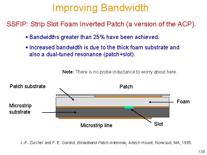
Improving Bandwidth SSFIP: Strip Slot Foam Inverted Patch (a version of the ACP). § Bandwidths greater than 25% have been achieved. § Increased bandwidth is due to the thick foam substrate and also a dual-tuned resonance (patch+slot). Note: There is no probe inductance to worry about here. Patch substrate Patch Foam Microstrip substrate Microstrip line Slot J. -F. Zürcher and F. E. Gardiol, Broadband Patch Antennas, Artech House, Norwood, MA, 1995. 138

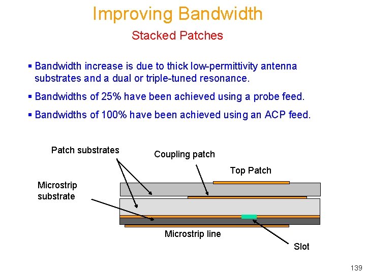
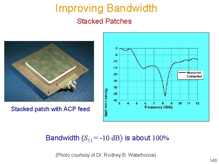
Improving Bandwidth Stacked Patches § Bandwidth increase is due to thick low-permittivity antenna substrates and a dual or triple-tuned resonance. § Bandwidths of 25% have been achieved using a probe feed. § Bandwidths of 100% have been achieved using an ACP feed. Patch substrates Coupling patch Top Patch Microstrip substrate Microstrip line Slot 139

Improving Bandwidth Stacked Patches Stacked patch with ACP feed Bandwidth (S 11 = -10 d. B) is about 100% (Photo courtesy of Dr. Rodney B. Waterhouse) 140

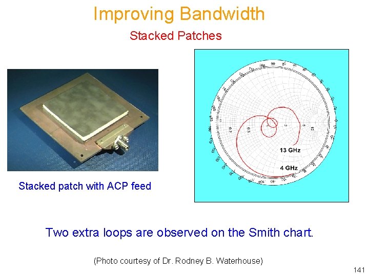
Improving Bandwidth Stacked Patches Stacked patch with ACP feed Two extra loops are observed on the Smith chart. (Photo courtesy of Dr. Rodney B. Waterhouse) 141

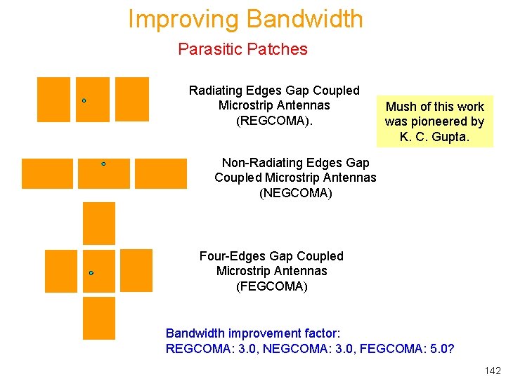
Improving Bandwidth Parasitic Patches Radiating Edges Gap Coupled Microstrip Antennas (REGCOMA). Mush of this work was pioneered by K. C. Gupta. Non-Radiating Edges Gap Coupled Microstrip Antennas (NEGCOMA) Four-Edges Gap Coupled Microstrip Antennas (FEGCOMA) Bandwidth improvement factor: REGCOMA: 3. 0, NEGCOMA: 3. 0, FEGCOMA: 5. 0? 142

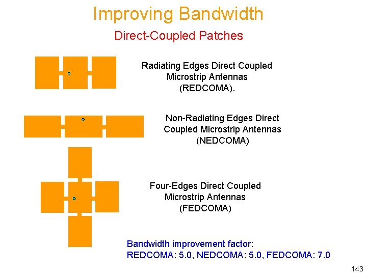
Improving Bandwidth Direct-Coupled Patches Radiating Edges Direct Coupled Microstrip Antennas (REDCOMA). Non-Radiating Edges Direct Coupled Microstrip Antennas (NEDCOMA) Four-Edges Direct Coupled Microstrip Antennas (FEDCOMA) Bandwidth improvement factor: REDCOMA: 5. 0, NEDCOMA: 5. 0, FEDCOMA: 7. 0 143

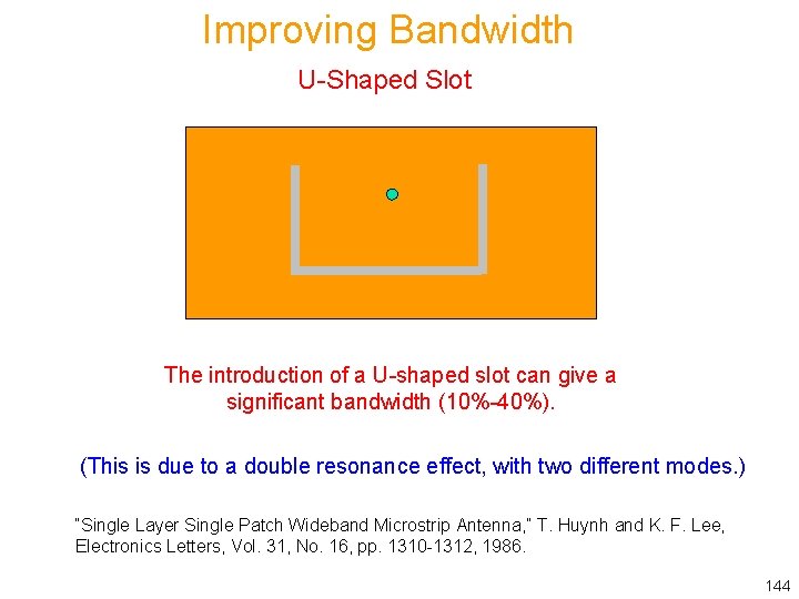
Improving Bandwidth U-Shaped Slot The introduction of a U-shaped slot can give a significant bandwidth (10%-40%). (This is due to a double resonance effect, with two different modes. ) “Single Layer Single Patch Wideband Microstrip Antenna, ” T. Huynh and K. F. Lee, Electronics Letters, Vol. 31, No. 16, pp. 1310 -1312, 1986. 144

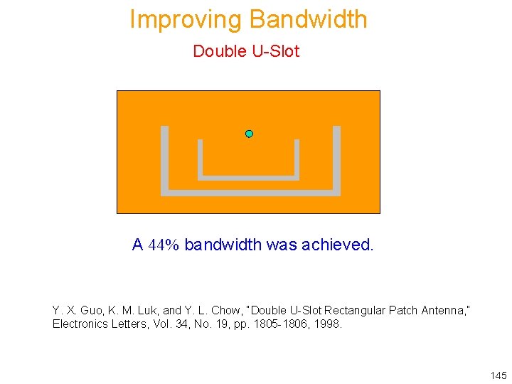
Improving Bandwidth Double U-Slot A 44% bandwidth was achieved. Y. X. Guo, K. M. Luk, and Y. L. Chow, “Double U-Slot Rectangular Patch Antenna, ” Electronics Letters, Vol. 34, No. 19, pp. 1805 -1806, 1998. 145

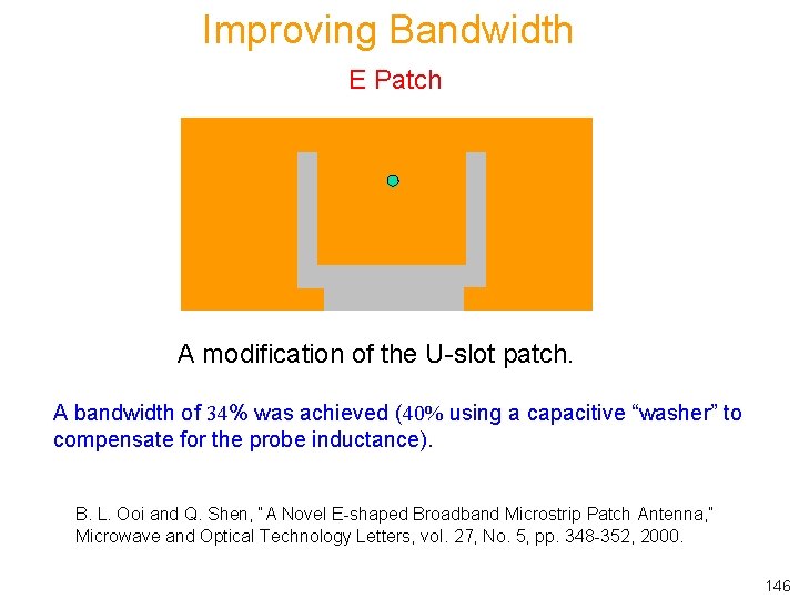
Improving Bandwidth E Patch A modification of the U-slot patch. A bandwidth of 34% was achieved (40% using a capacitive “washer” to compensate for the probe inductance). B. L. Ooi and Q. Shen, “A Novel E-shaped Broadband Microstrip Patch Antenna, ” Microwave and Optical Technology Letters, vol. 27, No. 5, pp. 348 -352, 2000. 146

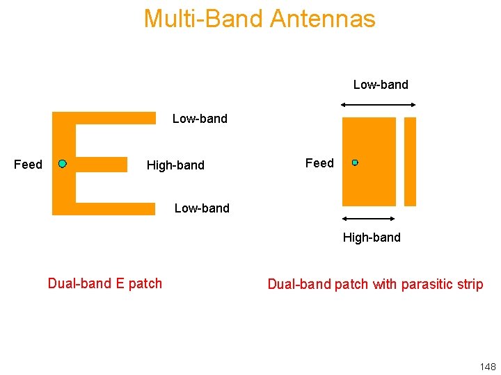
Multi-Band Antennas A multi-band antenna is sometimes more desirable than a broadband antenna, if multiple narrow-band channels are to be covered. General Principle: Introduce multiple resonance paths into the antenna. 147

Multi-Band Antennas Low-band Feed High-band Feed Low-band High-band Dual-band E patch Dual-band patch with parasitic strip 148

Outline v Overview of microstrip antennas v Feeding methods v Basic principles of operation v General characteristics v CAD Formulas v Radiation pattern v Input Impedance v Circular polarization v Circular patch v Improving bandwidth v Miniaturization v Reducing surface waves and lateral radiation 149

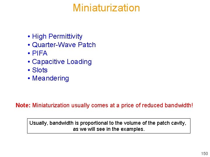
Miniaturization • High Permittivity • Quarter-Wave Patch • PIFA • Capacitive Loading • Slots • Meandering Note: Miniaturization usually comes at a price of reduced bandwidth! Usually, bandwidth is proportional to the volume of the patch cavity, as we will see in the examples. 150

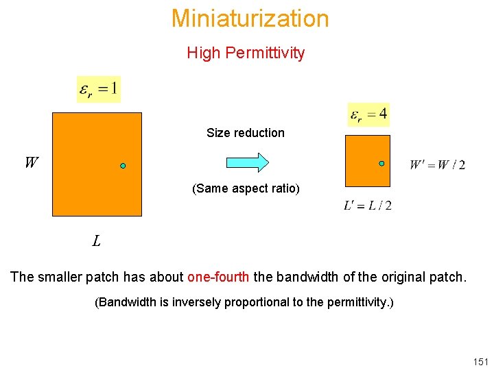
Miniaturization High Permittivity Size reduction W (Same aspect ratio) L The smaller patch has about one-fourth the bandwidth of the original patch. (Bandwidth is inversely proportional to the permittivity. ) 151

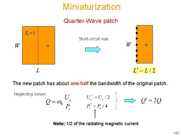
Miniaturization Quarter-Wave patch Ez = 0 Short-circuit vias W W L The new patch has about one-half the bandwidth of the original patch. Neglecting losses: Note: 1/2 of the radiating magnetic current 152

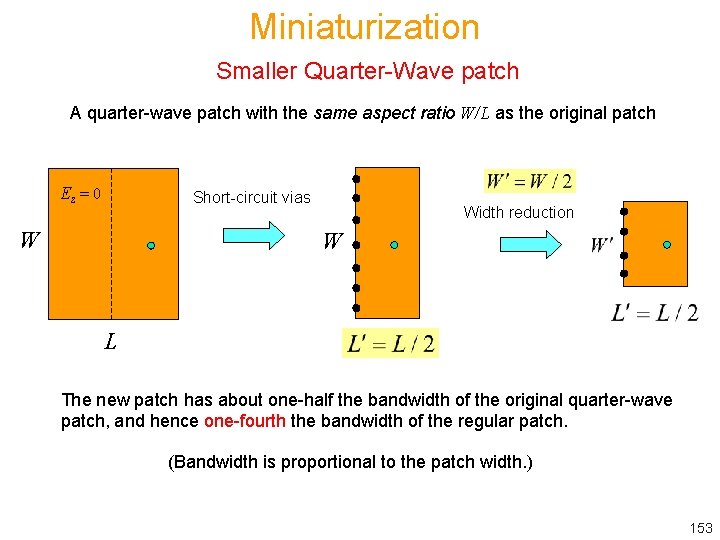
Miniaturization Smaller Quarter-Wave patch A quarter-wave patch with the same aspect ratio W/L as the original patch Ez = 0 Short-circuit vias W Width reduction W L The new patch has about one-half the bandwidth of the original quarter-wave patch, and hence one-fourth the bandwidth of the regular patch. (Bandwidth is proportional to the patch width. ) 153

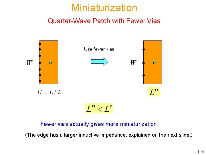
Miniaturization Quarter-Wave Patch with Fewer Vias Use fewer vias W W Fewer vias actually gives more miniaturization! (The edge has a larger inductive impedance: explained on the next slide. ) 154

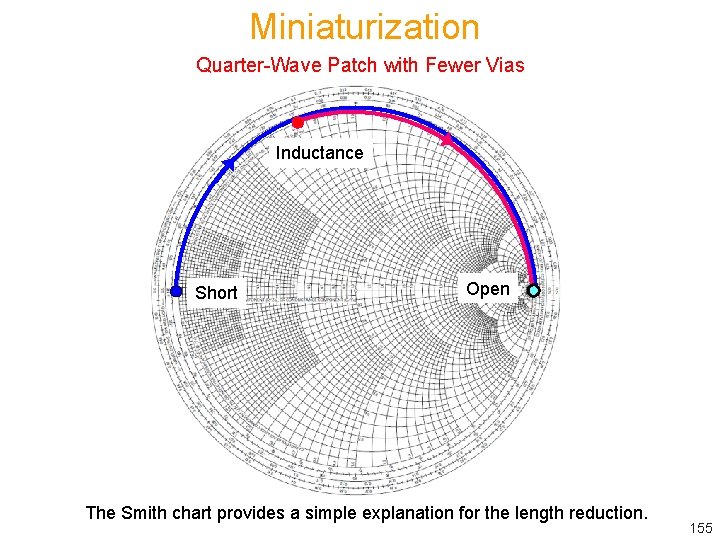
Miniaturization Quarter-Wave Patch with Fewer Vias Inductance Short Open The Smith chart provides a simple explanation for the length reduction. 155

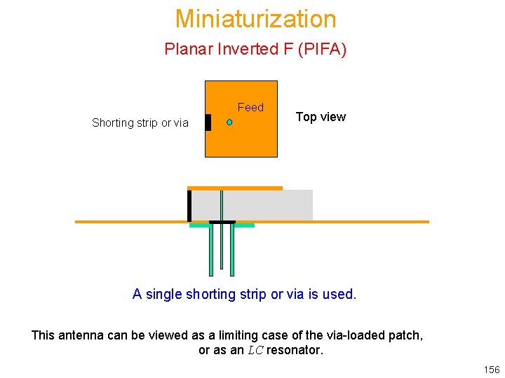
Miniaturization Planar Inverted F (PIFA) Feed Shorting strip or via Top view A single shorting strip or via is used. This antenna can be viewed as a limiting case of the via-loaded patch, or as an LC resonator. 156

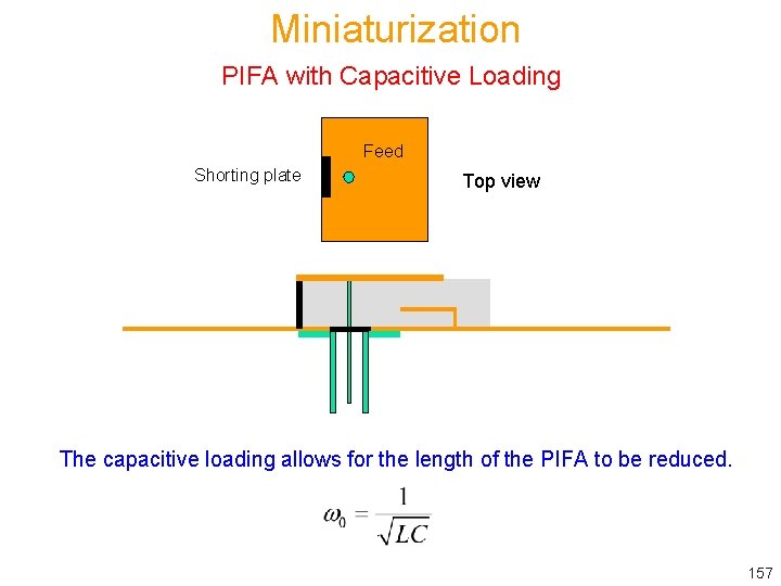
Miniaturization PIFA with Capacitive Loading Feed Shorting plate Top view The capacitive loading allows for the length of the PIFA to be reduced. 157

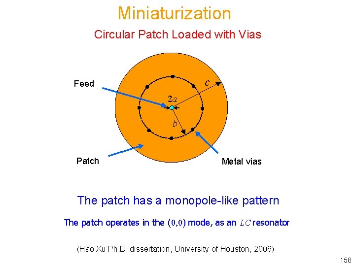
Miniaturization Circular Patch Loaded with Vias c Feed 2 a b Patch Metal vias The patch has a monopole-like pattern The patch operates in the (0, 0) mode, as an LC resonator (Hao Xu Ph. D. dissertation, University of Houston, 2006) 158

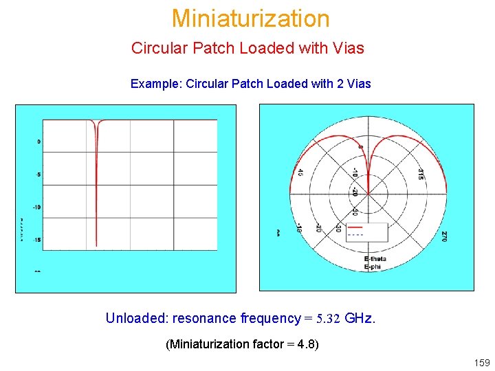
Miniaturization Circular Patch Loaded with Vias Example: Circular Patch Loaded with 2 Vias Unloaded: resonance frequency = 5. 32 GHz. (Miniaturization factor = 4. 8) 159

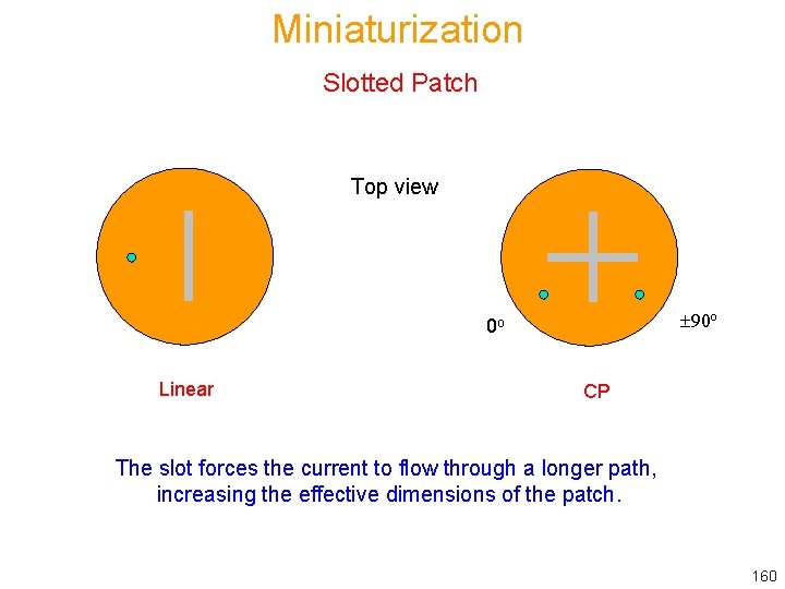
Miniaturization Slotted Patch Top view 90 o 0 o Linear CP The slot forces the current to flow through a longer path, increasing the effective dimensions of the patch. 160

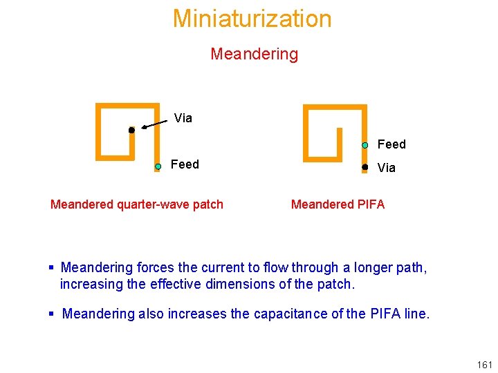
Miniaturization Meandering Via Feed Meandered quarter-wave patch Via Meandered PIFA § Meandering forces the current to flow through a longer path, increasing the effective dimensions of the patch. § Meandering also increases the capacitance of the PIFA line. 161

Outline v Overview of microstrip antennas v Feeding methods v Basic principles of operation v General characteristics v CAD Formulas v Input Impedance v Radiation pattern v Circular polarization v Circular patch v Improving bandwidth v Miniaturization v Reducing surface waves and lateral radiation 162

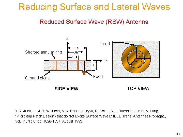
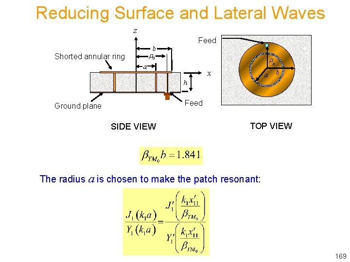
Reducing Surface and Lateral Waves Reduced Surface Wave (RSW) Antenna z Feed b r 0 Shorted annular ring ro a x a b h Feed Ground plane SIDE VIEW TOP VIEW D. R. Jackson, J. T. Williams, A. K. Bhattacharyya, R. Smith, S. J. Buchheit, and S. A. Long, “Microstrip Patch Designs that do Not Excite Surface Waves, ” IEEE Trans. Antennas Propagat. , vol. 41, No 8, pp. 1026 -1037, August 1993. 163

Reducing Surface and Lateral Waves Reducing surface-wave excitation and lateral radiation reduces edge diffraction and mutual coupling. Ø Edge diffraction degrades the radiation pattern on a finite ground plane. Ø Mutual coupling causes an desirable coupling between antennas. 164

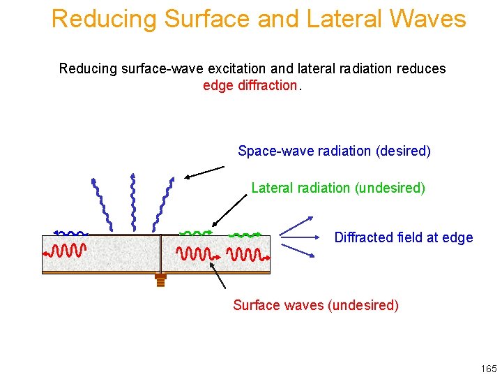
Reducing Surface and Lateral Waves Reducing surface-wave excitation and lateral radiation reduces edge diffraction. Space-wave radiation (desired) Lateral radiation (undesired) Diffracted field at edge Surface waves (undesired) 165

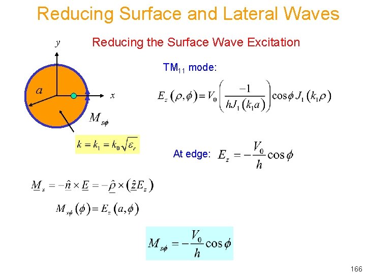
Reducing Surface and Lateral Waves y Reducing the Surface Wave Excitation TM 11 mode: a x At edge: 166

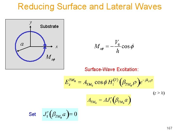
Reducing Surface and Lateral Waves y a Substrate x Surface-Wave Excitation: (z > h) Set 167

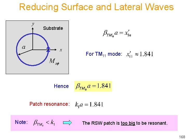
Reducing Surface and Lateral Waves y a Substrate x For TM 11 mode: Hence Patch resonance: Note: The RSW patch is too big to be resonant. 168

Reducing Surface and Lateral Waves z Feed b r 0 Shorted annular ring ro a x a b h Feed Ground plane SIDE VIEW TOP VIEW The radius a is chosen to make the patch resonant: 169

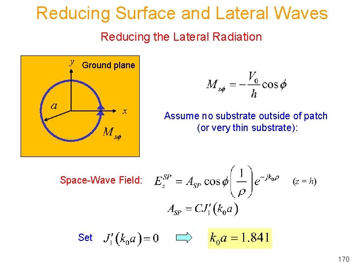
Reducing Surface and Lateral Waves Reducing the Lateral Radiation y Ground plane a x Space-Wave Field: Assume no substrate outside of patch (or very thin substrate): (z = h) Set 170

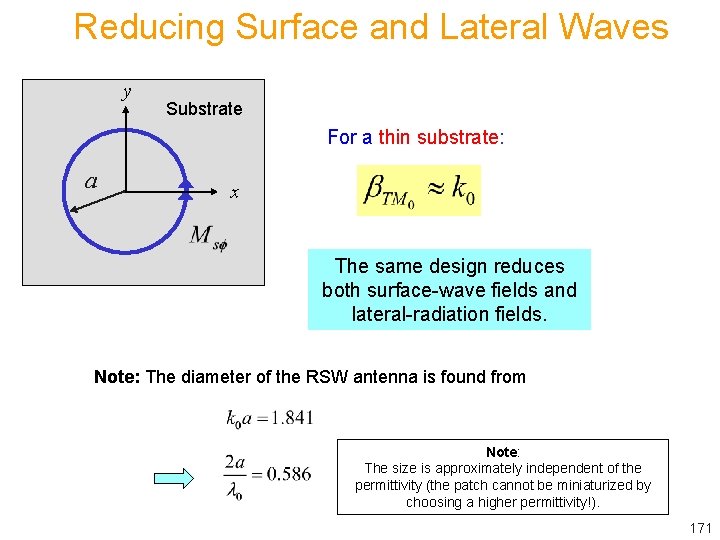
Reducing Surface and Lateral Waves y Substrate For a thin substrate: a x The same design reduces both surface-wave fields and lateral-radiation fields. Note: The diameter of the RSW antenna is found from Note: The size is approximately independent of the permittivity (the patch cannot be miniaturized by choosing a higher permittivity!). 171

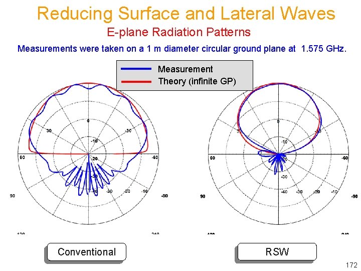
Reducing Surface and Lateral Waves E-plane Radiation Patterns Measurements were taken on a 1 m diameter circular ground plane at 1. 575 GHz. Measurement Theory (infinite GP) Conventional RSW 172

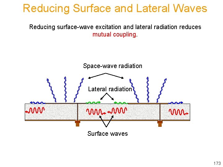
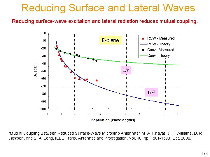
Reducing Surface and Lateral Waves Reducing surface-wave excitation and lateral radiation reduces mutual coupling. Space-wave radiation Lateral radiation Surface waves 173

Reducing Surface and Lateral Waves Reducing surface-wave excitation and lateral radiation reduces mutual coupling. E-plane 1/r 3 “Mutual Coupling Between Reduced Surface-Wave Microstrip Antennas, ” M. A. Khayat, J. T. Williams, D. R. Jackson, and S. A. Long, IEEE Trans. Antennas and Propagation, Vol. 48, pp. 1581 -1593, Oct. 2000. 174

References General references about microstrip antennas: Microstrip Patch Antennas, K. F. Fong Lee and K. M. Luk, Imperial College Press, 2011. Microstrip and Patch Antennas Design, 2 nd Ed. , R. Bancroft, Scitech Publishing, 2009. Microstrip Patch Antennas: A Designer’s Guide, R. B. Waterhouse, Kluwer Academic Publishers, 2003. Microstrip Antenna Design Handbook, R. Garg, P. Bhartia, I. J. Bahl, and A. Ittipiboon, Editors, Artech House, 2001. Advances in Microstrip and Printed Antennas, K. F. Lee, Editor, John Wiley, 1997. 175

References (cont. ) General references about microstrip antennas (cont. ): CAD of Microstrip Antennas for Wireless Applications, R. A. Sainati, Artech House, 1996. Microstrip Antennas: The Analysis and Design of Microstrip Antennas and Arrays, D. M. Pozar and D. H. Schaubert, Editors, Wiley/IEEE Press, 1995. Millimeter-Wave Microstrip and Printed Circuit Antennas, P. Bhartia, Artech House, 1991. The Handbook of Microstrip Antennas (two volume set), J. R. James and P. S. Hall, INSPEC, 1989. Microstrip Antenna Theory and Design, J. R. James, P. S. Hall, and C. Wood, INSPEC/IEE, 1981. 176

References (cont. ) More information about the CAD formulas presented here for the rectangular patch may be found in: Microstrip Antennas, D. R. Jackson, Ch. 7 of Antenna Engineering Handbook, J. L. Volakis, Editor, Mc. Graw Hill, 2007. Computer-Aided Design of Rectangular Microstrip Antennas, D. R. Jackson, S. A. Long, J. T. Williams, and V. B. Davis, Ch. 5 of Advances in Microstrip and Printed Antennas, K. F. Lee, Editor, John Wiley, 1997. 177

References (cont. ) References devoted to broadband microstrip antennas: Compact and Broadband Microstrip Antennas, K. -L. Wong, John Wiley, 2003. Broadband Microstrip Antennas, G. Kumar and K. P. Ray, Artech House, 2002. Broadband Patch Antennas, J. -F. Zürcher and F. E. Gardiol, Artech House, 1995. 178

The End 179