Introduction to microfabrication of solid state devices Maksym
Introduction to microfabrication of solid state devices Maksym Myronov Department of Physics, The University of Warwick, Coventry CV 4 7 AL, UK October - November 2019
Lectures outline 1. Introduction 2. Clean rooms 3. Materials and substrates 4. Pattern transfer 5. Etching 6. Thin films deposition 7. Thermal treatments 8. Metrology Maksym Myronov - Introduction to microfabrication of solid state devices - 2019 2
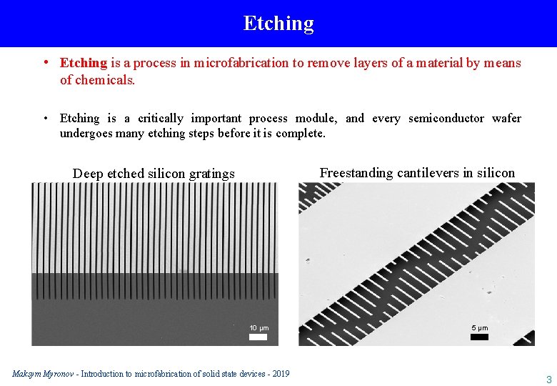
Etching • Etching is a process in microfabrication to remove layers of a material by means of chemicals. • Etching is a critically important process module, and every semiconductor wafer undergoes many etching steps before it is complete. Freestanding cantilevers in silicon Deep etched silicon gratings 10 µm Maksym Myronov - Introduction to microfabrication of solid state devices - 2019 5 µm 3
Etching terminology Etching mask – patterned protective layer on the top of etched material Undercut – lateral erosion of etched material below protective layer Selectivity – ratio of etching rates for two etched materials Aspect ration – ratio of height to width for a microstructure Anisotropy – different etching rate in different directions Maksym Myronov - Introduction to microfabrication of solid state devices - 2019 4
Etching mask • For many etch steps, part of the wafer is protected from the etchant by a "masking" material which resists etching. • In some cases, the masking material is a photoresist which has been patterned using photolithography. • Aggressive etchants like (KOH) will prevent use of resist. Due to this another mask is required. • Other situations require a more durable mask, such as Si. O 2 or Si 3 N 4. Maksym Myronov - Introduction to microfabrication of solid state devices - 2019 5
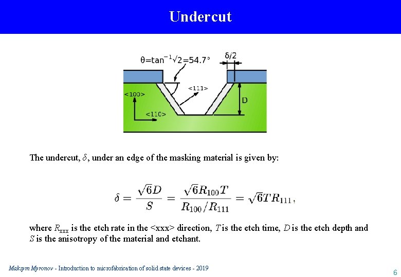
Undercut The undercut, δ, under an edge of the masking material is given by: where Rxxx is the etch rate in the <xxx> direction, T is the etch time, D is the etch depth and S is the anisotropy of the material and etchant. Maksym Myronov - Introduction to microfabrication of solid state devices - 2019 6
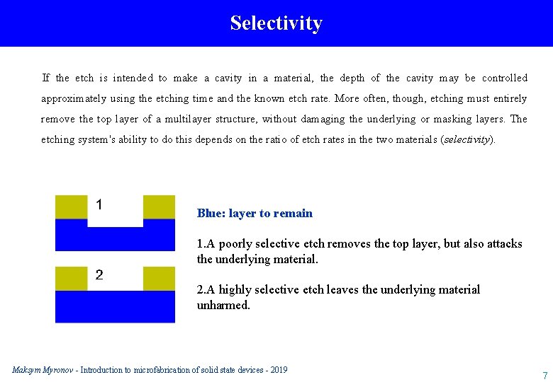
Selectivity If the etch is intended to make a cavity in a material, the depth of the cavity may be controlled approximately using the etching time and the known etch rate. More often, though, etching must entirely remove the top layer of a multilayer structure, without damaging the underlying or masking layers. The etching system's ability to do this depends on the ratio of etch rates in the two materials (selectivity). Blue: layer to remain 1. A poorly selective etch removes the top layer, but also attacks the underlying material. 2. A highly selective etch leaves the underlying material unharmed. Maksym Myronov - Introduction to microfabrication of solid state devices - 2019 7
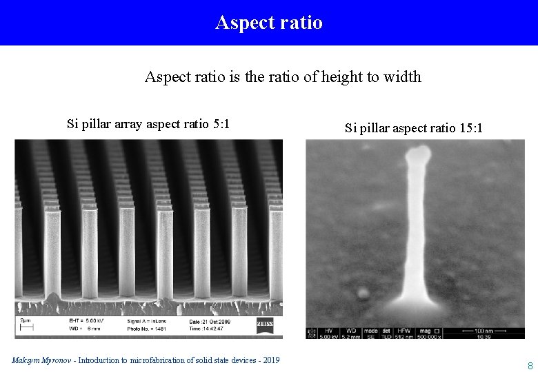
Aspect ratio is the ratio of height to width Si pillar array aspect ratio 5: 1 Maksym Myronov - Introduction to microfabrication of solid state devices - 2019 Si pillar aspect ratio 15: 1 8
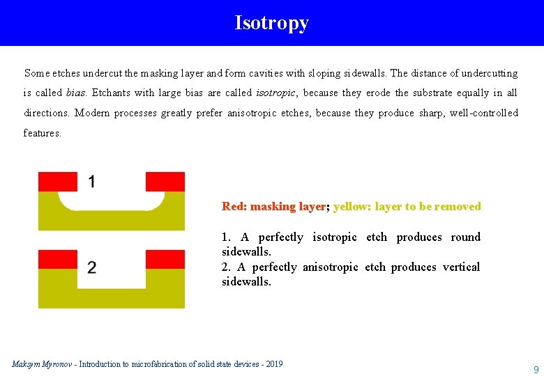
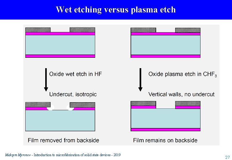
Isotropy Some etches undercut the masking layer and form cavities with sloping sidewalls. The distance of undercutting is called bias. Etchants with large bias are called isotropic, because they erode the substrate equally in all directions. Modern processes greatly prefer anisotropic etches, because they produce sharp, well-controlled features. Red: masking layer; yellow: layer to be removed 1. A perfectly isotropic etch produces round sidewalls. 2. A perfectly anisotropic etch produces vertical sidewalls. Maksym Myronov - Introduction to microfabrication of solid state devices - 2019 9
Etching media and technology Two fundamental types of etchants are liquid-phase ("wet") and plasma-phase ("dry"). 1) Wet etching where the material is dissolved when immersed in a chemical solution solid+ liquid etchant soluble products 2) Dry etching where the material is sputtered or dissolved using reactive ions or a vapor phase etchant solid + gaseous etchant volatile products Each of these exists in several varieties. Typical etching rate 100 – 1000 nm/min in both cases Maksym Myronov - Introduction to microfabrication of solid state devices - 2019 10
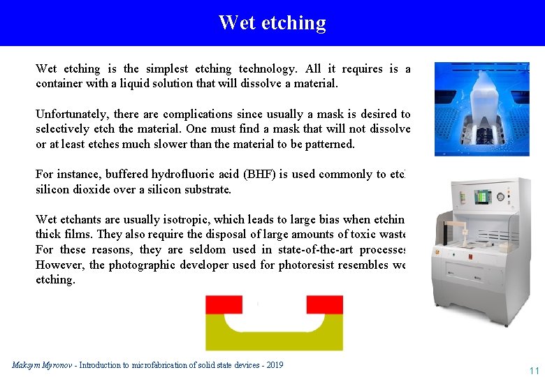
Wet etching is the simplest etching technology. All it requires is a container with a liquid solution that will dissolve a material. Unfortunately, there are complications since usually a mask is desired to selectively etch the material. One must find a mask that will not dissolve or at least etches much slower than the material to be patterned. For instance, buffered hydrofluoric acid (BHF) is used commonly to etch silicon dioxide over a silicon substrate. Wet etchants are usually isotropic, which leads to large bias when etching thick films. They also require the disposal of large amounts of toxic waste. For these reasons, they are seldom used in state-of-the-art processes. However, the photographic developer used for photoresist resembles wet etching. Maksym Myronov - Introduction to microfabrication of solid state devices - 2019 11
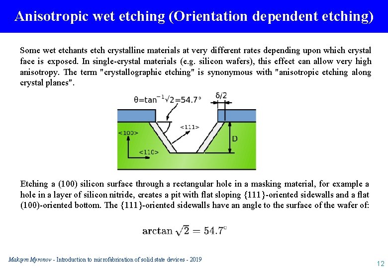
Anisotropic wet etching (Orientation dependent etching) Some wet etchants etch crystalline materials at very different rates depending upon which crystal face is exposed. In single-crystal materials (e. g. silicon wafers), this effect can allow very high anisotropy. The term "crystallographic etching" is synonymous with "anisotropic etching along crystal planes". Etching a (100) silicon surface through a rectangular hole in a masking material, for example a hole in a layer of silicon nitride, creates a pit with flat sloping {111}-oriented sidewalls and a flat (100)-oriented bottom. The {111}-oriented sidewalls have an angle to the surface of the wafer of: Maksym Myronov - Introduction to microfabrication of solid state devices - 2019 12
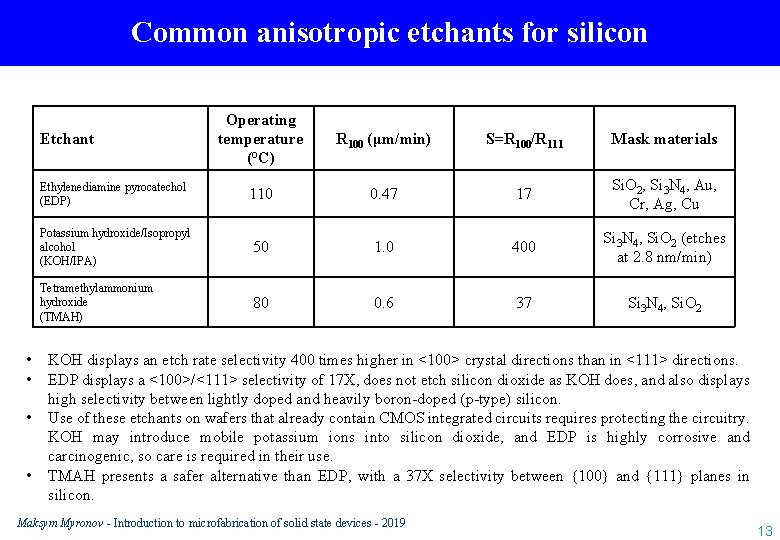
Common anisotropic etchants for silicon Operating temperature (°C) R 100 (μm/min) S=R 100/R 111 Mask materials Ethylenediamine pyrocatechol (EDP) 110 0. 47 17 Si. O 2, Si 3 N 4, Au, Cr, Ag, Cu Potassium hydroxide/Isopropyl alcohol (KOH/IPA) 50 1. 0 400 Si 3 N 4, Si. O 2 (etches at 2. 8 nm/min) Tetramethylammonium hydroxide (TMAH) 80 0. 6 37 Si 3 N 4, Si. O 2 Etchant • • KOH displays an etch rate selectivity 400 times higher in <100> crystal directions than in <111> directions. EDP displays a <100>/<111> selectivity of 17 X, does not etch silicon dioxide as KOH does, and also displays high selectivity between lightly doped and heavily boron-doped (p-type) silicon. Use of these etchants on wafers that already contain CMOS integrated circuits requires protecting the circuitry. KOH may introduce mobile potassium ions into silicon dioxide, and EDP is highly corrosive and carcinogenic, so care is required in their use. TMAH presents a safer alternative than EDP, with a 37 X selectivity between {100} and {111} planes in silicon. Maksym Myronov - Introduction to microfabrication of solid state devices - 2019 13
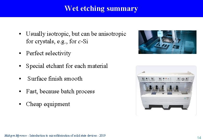
Wet etching summary • Usually isotropic, but can be anisotropic for crystals, e. g. , for c-Si • Perfect selectivity • Special etchant for each material • Surface finish smooth • Fast, because batch process • Cheap equipment Maksym Myronov - Introduction to microfabrication of solid state devices - 2019 14
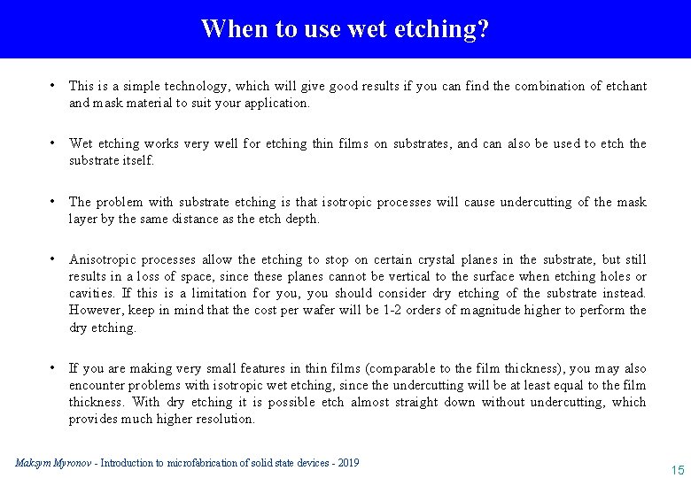
When to use wet etching? • This is a simple technology, which will give good results if you can find the combination of etchant and mask material to suit your application. • Wet etching works very well for etching thin films on substrates, and can also be used to etch the substrate itself. • The problem with substrate etching is that isotropic processes will cause undercutting of the mask layer by the same distance as the etch depth. • Anisotropic processes allow the etching to stop on certain crystal planes in the substrate, but still results in a loss of space, since these planes cannot be vertical to the surface when etching holes or cavities. If this is a limitation for you, you should consider dry etching of the substrate instead. However, keep in mind that the cost per wafer will be 1 -2 orders of magnitude higher to perform the dry etching. • If you are making very small features in thin films (comparable to the film thickness), you may also encounter problems with isotropic wet etching, since the undercutting will be at least equal to the film thickness. With dry etching it is possible etch almost straight down without undercutting, which provides much higher resolution. Maksym Myronov - Introduction to microfabrication of solid state devices - 2019 15
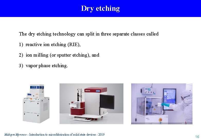
Dry etching The dry etching technology can split in three separate classes called 1) reactive ion etching (RIE), 2) ion milling (or sputter etching), and 3) vapor phase etching. Maksym Myronov - Introduction to microfabrication of solid state devices - 2019 16
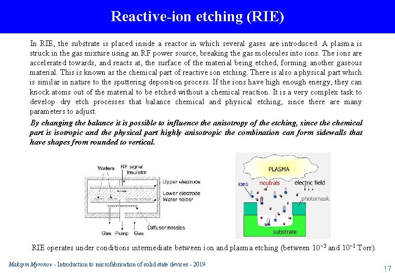
Reactive-ion etching (RIE) In RIE, the substrate is placed inside a reactor in which several gases are introduced. A plasma is struck in the gas mixture using an RF power source, breaking the gas molecules into ions. The ions are accelerated towards, and reacts at, the surface of the material being etched, forming another gaseous material. This is known as the chemical part of reactive ion etching. There is also a physical part which is similar in nature to the sputtering deposition process. If the ions have high enough energy, they can knock atoms out of the material to be etched without a chemical reaction. It is a very complex task to develop dry etch processes that balance chemical and physical etching, since there are many parameters to adjust. By changing the balance it is possible to influence the anisotropy of the etching, since the chemical part is isotropic and the physical part highly anisotropic the combination can form sidewalls that have shapes from rounded to vertical. RIE operates under conditions intermediate between ion and plasma etching (between 10− 3 and 10− 1 Torr). Maksym Myronov - Introduction to microfabrication of solid state devices - 2019 17
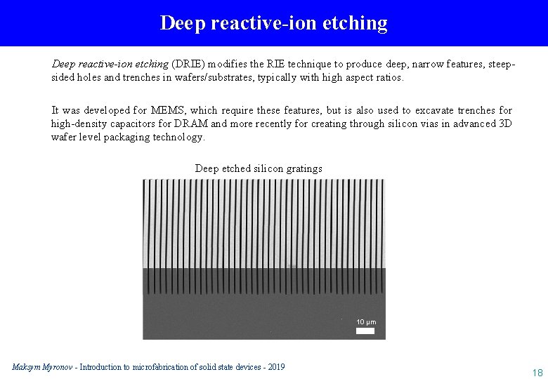
Deep reactive-ion etching (DRIE) modifies the RIE technique to produce deep, narrow features, steepsided holes and trenches in wafers/substrates, typically with high aspect ratios. It was developed for MEMS, which require these features, but is also used to excavate trenches for high-density capacitors for DRAM and more recently for creating through silicon vias in advanced 3 D wafer level packaging technology. Deep etched silicon gratings 10 µm Maksym Myronov - Introduction to microfabrication of solid state devices - 2019 18
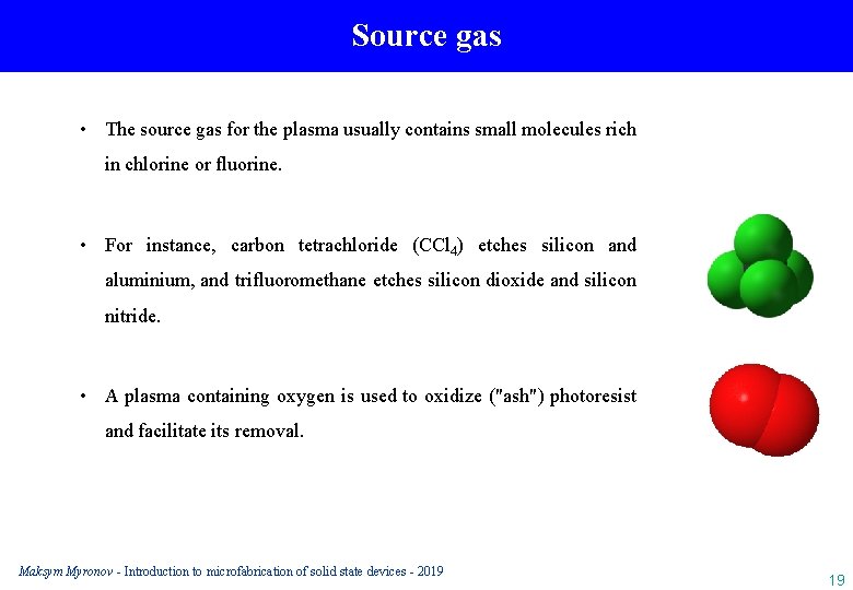
Source gas • The source gas for the plasma usually contains small molecules rich in chlorine or fluorine. • For instance, carbon tetrachloride (CCl 4) etches silicon and aluminium, and trifluoromethane etches silicon dioxide and silicon nitride. • A plasma containing oxygen is used to oxidize ("ash") photoresist and facilitate its removal. Maksym Myronov - Introduction to microfabrication of solid state devices - 2019 19
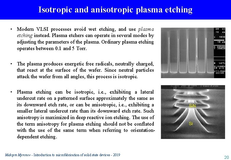
Isotropic and anisotropic plasma etching • Modern VLSI processes avoid wet etching, and use plasma etching instead. Plasma etchers can operate in several modes by adjusting the parameters of the plasma. Ordinary plasma etching operates between 0. 1 and 5 Torr. • The plasma produces energetic free radicals, neutrally charged, that react at the surface of the wafer. Since neutral particles attack the wafer from all angles, this process is isotropic. • Plasma etching can be isotropic, i. e. , exhibiting a lateral undercut rate on a patterned surface approximately the same as its downward etch rate, or can be anisotropic, i. e. , exhibiting a smaller lateral undercut rate than its downward etch rate. Such anisotropy is maximized in deep reactive ion etching. The use of the term anisotropy for plasma etching should not be conflated with the use of the same term when referring to orientationdependent etching. Maksym Myronov - Introduction to microfabrication of solid state devices - 2019 20
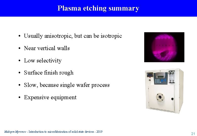
Plasma etching summary • Usually anisotropic, but can be isotropic • Near vertical walls • Low selectivity • Surface finish rough • Slow, because single wafer process • Expensive equipment Maksym Myronov - Introduction to microfabrication of solid state devices - 2019 21
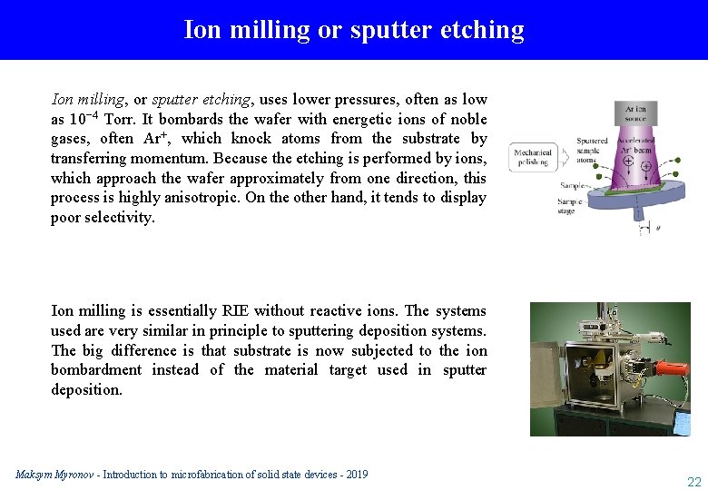
Ion milling or sputter etching Ion milling, or sputter etching, uses lower pressures, often as low as 10− 4 Torr. It bombards the wafer with energetic ions of noble gases, often Ar+, which knock atoms from the substrate by transferring momentum. Because the etching is performed by ions, which approach the wafer approximately from one direction, this process is highly anisotropic. On the other hand, it tends to display poor selectivity. Ion milling is essentially RIE without reactive ions. The systems used are very similar in principle to sputtering deposition systems. The big difference is that substrate is now subjected to the ion bombardment instead of the material target used in sputter deposition. Maksym Myronov - Introduction to microfabrication of solid state devices - 2019 22
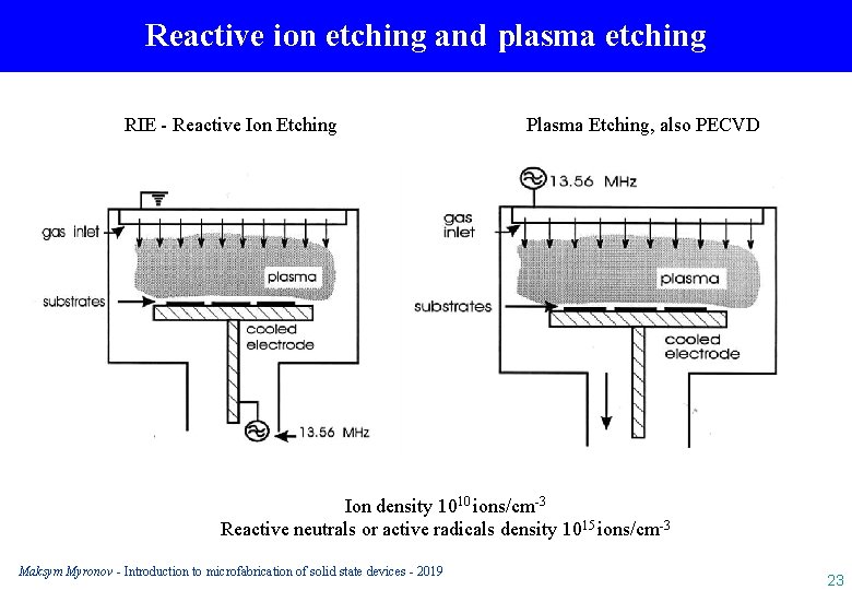
Reactive ion etching and plasma etching RIE - Reactive Ion Etching Plasma Etching, also PECVD Ion density 1010 ions/cm-3 Reactive neutrals or active radicals density 1015 ions/cm-3 Maksym Myronov - Introduction to microfabrication of solid state devices - 2019 23
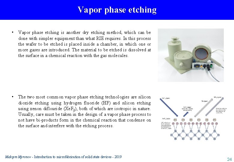
Vapor phase etching • Vapor phase etching is another dry etching method, which can be done with simpler equipment than what RIE requires. In this process the wafer to be etched is placed inside a chamber, in which one or more gases are introduced. The material to be etched is dissolved at the surface in a chemical reaction with the gas molecules. • The two most common vapor phase etching technologies are silicon dioxide etching using hydrogen fluoride (HF) and silicon etching using xenon diflouride (Xe. F 2), both of which are isotropic in nature. Usually, care must be taken in the design of a vapor phase process to not have bi-products form in the chemical reaction that condense on the surface and interfere with the etching process. Maksym Myronov - Introduction to microfabrication of solid state devices - 2019 24
When to use dry etching? • The first thing you should note about this technology is that it is expensive to run compared to wet etching. • If you are concerned with feature resolution in thin film structures or you need vertical sidewalls for deep etchings in the substrate, you have to consider dry etching. • If you are concerned about the price of your process and device, you may want to minimize the use of dry etching. • The IC industry has long since adopted dry etching to achieve small features, but in many cases feature size is not as critical in microfabrication. • Dry etching is an enabling technology, which comes at a sometimes high cost. Maksym Myronov - Introduction to microfabrication of solid state devices - 2019 25
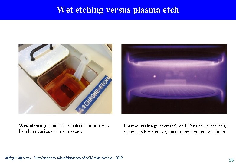
Wet etching versus plasma etch Wet etching: chemical reaction; simple wet bench and acids or bases needed Maksym Myronov - Introduction to microfabrication of solid state devices - 2019 Plasma etching: chemical and physical processes; requires RF-generator, vacuum system and gas lines 26
Wet etching versus plasma etch Maksym Myronov - Introduction to microfabrication of solid state devices - 2019 27
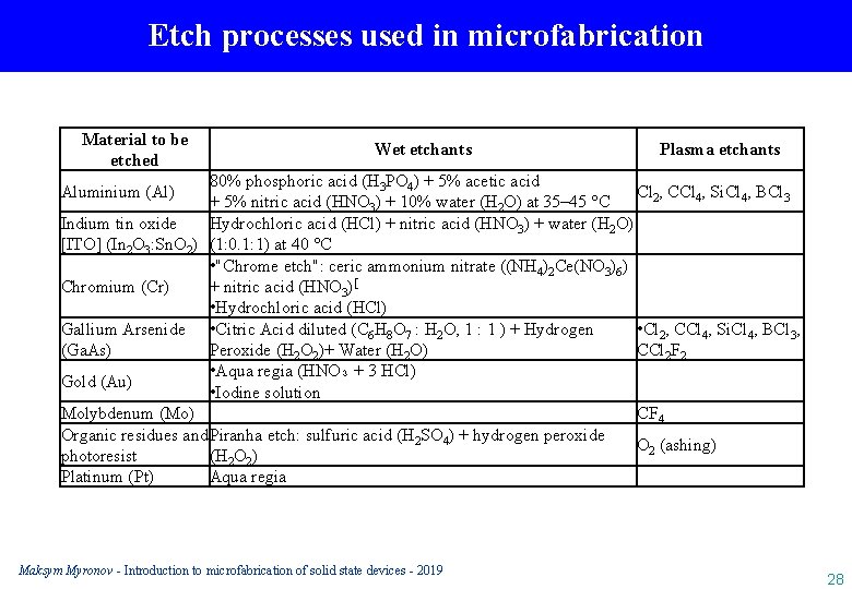
Etch processes used in microfabrication Material to be etched Wet etchants Plasma etchants 80% phosphoric acid (H 3 PO 4) + 5% acetic acid Cl 2, CCl 4, Si. Cl 4, BCl 3 + 5% nitric acid (HNO 3) + 10% water (H 2 O) at 35– 45 °C Indium tin oxide Hydrochloric acid (HCl) + nitric acid (HNO 3) + water (H 2 O) [ITO] (In 2 O 3: Sn. O 2) (1: 0. 1: 1) at 40 °C • "Chrome etch": ceric ammonium nitrate ((NH 4)2 Ce(NO 3)6) Chromium (Cr) + nitric acid (HNO 3)[ • Hydrochloric acid (HCl) Gallium Arsenide • Citric Acid diluted (C 6 H 8 O 7 : H 2 O, 1 : 1 ) + Hydrogen • Cl 2, CCl 4, Si. Cl 4, BCl 3, (Ga. As) Peroxide (H 2 O 2)+ Water (H 2 O) CCl 2 F 2 • Aqua regia (HNO₃ + 3 HCl) Gold (Au) • Iodine solution Molybdenum (Mo) CF 4 Organic residues and Piranha etch: sulfuric acid (H 2 SO 4) + hydrogen peroxide O 2 (ashing) photoresist (H 2 O 2) Platinum (Pt) Aqua regia Aluminium (Al) Maksym Myronov - Introduction to microfabrication of solid state devices - 2019 28
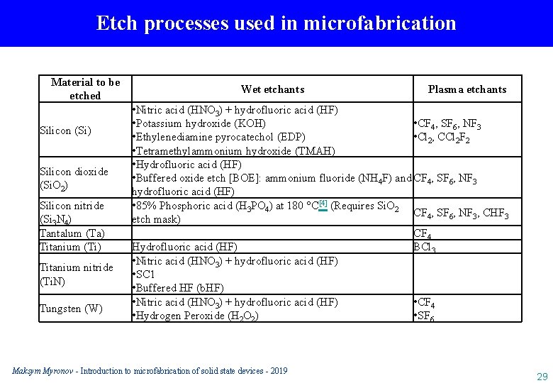
Etch processes used in microfabrication Material to be etched Silicon (Si) Silicon dioxide (Si. O 2) Silicon nitride (Si 3 N 4) Tantalum (Ta) Titanium (Ti) Titanium nitride (Ti. N) Tungsten (W) Wet etchants Plasma etchants • Nitric acid (HNO 3) + hydrofluoric acid (HF) • Potassium hydroxide (KOH) • CF 4, SF 6, NF 3 • Ethylenediamine pyrocatechol (EDP) • Cl 2, CCl 2 F 2 • Tetramethylammonium hydroxide (TMAH) • Hydrofluoric acid (HF) • Buffered oxide etch [BOE]: ammonium fluoride (NH 4 F) and CF 4, SF 6, NF 3 hydrofluoric acid (HF) • 85% Phosphoric acid (H 3 PO 4) at 180 °C[4] (Requires Si. O 2 CF 4, SF 6, NF 3, CHF 3 etch mask) CF 4 Hydrofluoric acid (HF) BCl 3 • Nitric acid (HNO 3) + hydrofluoric acid (HF) • SC 1 • Buffered HF (b. HF) • Nitric acid (HNO 3) + hydrofluoric acid (HF) • CF 4 • Hydrogen Peroxide (H 2 O 2) • SF 6 Maksym Myronov - Introduction to microfabrication of solid state devices - 2019 29

Summary Maksym Myronov - Introduction to microfabrication of solid state devices - 2019 30
- Slides: 30