INTRODUCTION TO LOGIC DESIGN Chapter 3 GateLevel Minimazation










- Slides: 92

INTRODUCTION TO LOGIC DESIGN Chapter 3 Gate-Level Minimazation gürtaçyemişçioğlu

2 OUTLINE OF CHAPTER 1 The Map Method Four – Variable K-Map Product of Sums Simplification Don’t Care Conditions NAND and NOR Implementations Other Two Level Implementations Exclusive-OR Function Hardware Description Language 26 September 2020 INTRODUCTION TO LOGIC DESIGN

3. 1 THE MAP METHOD

THE MAP METHOD • Gate-level minimization refers to the design task of finding an optimal gate-level implementation of Boolean functions describing a digital circuit. 26 September 2020 INTRODUCTION TO LOGIC DESIGN 4

THE MAP METHOD • The complexity of the digital logic gates – The complexity of the algebraic expression • Logic minimization – Algebraic approaches: lack of specific rules – The Karnaugh map • A simple straight forward procedure • A pictorial form of a truth table • Applicable if the # of variables < 7 26 September 2020 INTRODUCTION TO LOGIC DESIGN 5

THE MAP METHOD • A diagram made up of squares – Each square represents one minterm • The simplified expression produced by the map are always in one of the two standard forms: – Sum of products – Product of sums 26 September 2020 INTRODUCTION TO LOGIC DESIGN 6

THE MAP METHOD • Boolean function – Sum of minterms – Sum of products (or product of sum) in the simplest form – A minimum number of terms – A minimum number of literals – The simplified expression may not be unique 26 September 2020 INTRODUCTION TO LOGIC DESIGN 7

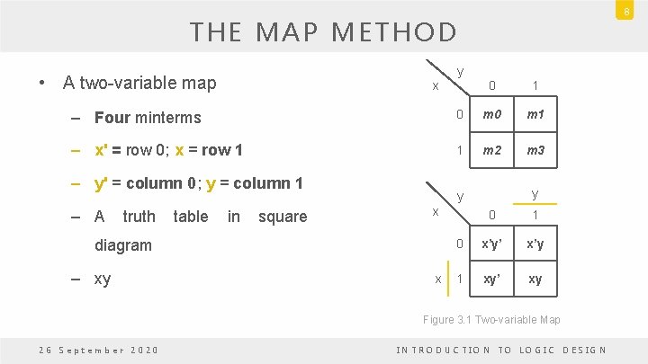
8 THE MAP METHOD • A two-variable map y x 0 1 – Four minterms 0 m 1 – x' = row 0; x = row 1 1 m 2 m 3 – y' = column 0; y = column 1 – A truth table in square x diagram – xy y y x 0 1 0 x’y’ x’y 1 xy’ xy Figure 3. 1 Two-variable Map 26 September 2020 INTRODUCTION TO LOGIC DESIGN

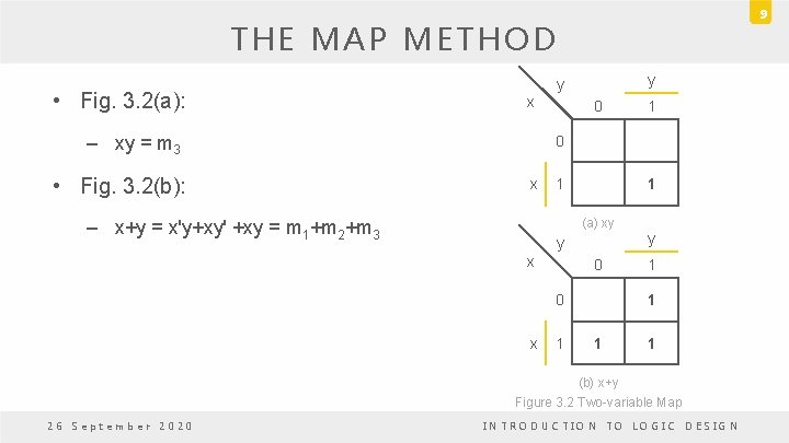
9 THE MAP METHOD • Fig. 3. 2(a): x – xy = m 3 • Fig. 3. 2(b): y y 0 1 0 x 1 1 (a) xy – x+y = x'y+xy' +xy = m 1+m 2+m 3 y x 0 0 x 1 y 1 1 (b) x+y Figure 3. 2 Two-variable Map 26 September 2020 INTRODUCTION TO LOGIC DESIGN

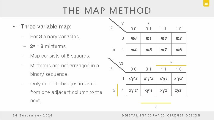
10 THE MAP METHOD • Three-variable map: y y X – For 3 binary variables. – 2 n = 8 minterms. x 0 0 0 1 1 0 0 m 1 m 3 m 2 1 m 4 m 5 m 7 m 6 – Map consists of 8 squares. – Minterms are not arranged in a x binary sequence. – Only one bit changes in value from one adjacent column to the y yz x 0 0 0 1 1 0 0 x’y’z’ x’y’z x’yz’ 1 xy’z’ xy’z xyz’ next. z 26 September 2020 DIGITAL INTEGRATED CIRCUIT DESIGN

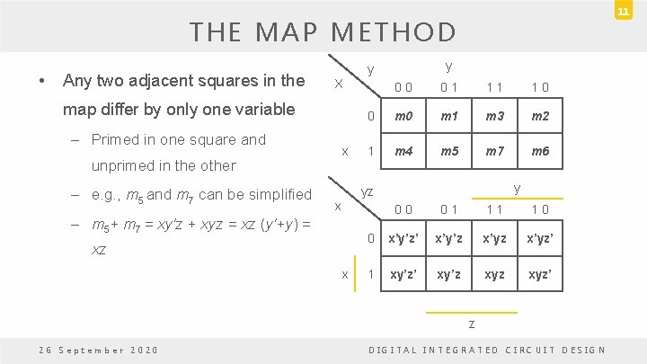
11 THE MAP METHOD • Any two adjacent squares in the X map differ by only one variable – Primed in one square and x unprimed in the other – e. g. , m 5 and m 7 can be simplified y y 0 0 0 1 1 0 0 m 1 m 3 m 2 1 m 4 m 5 m 7 m 6 y yz x – m 5+ m 7 = xy'z + xyz = xz (y'+y) = xz x 0 0 0 1 1 0 0 x’y’z’ x’y’z x’yz’ 1 xy’z’ xy’z xyz’ z 26 September 2020 DIGITAL INTEGRATED CIRCUIT DESIGN

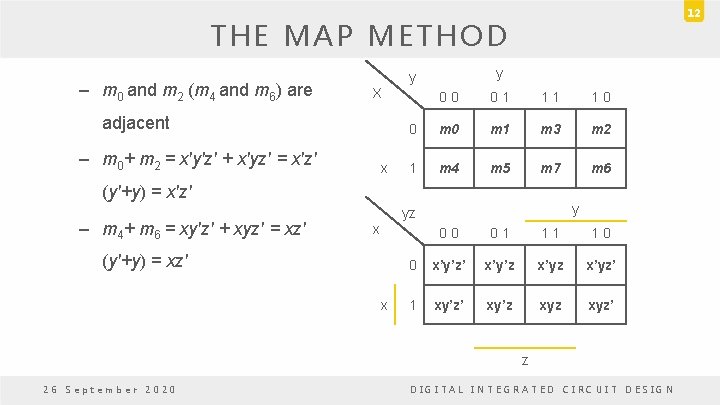
12 THE MAP METHOD – m 0 and m 2 (m 4 and m 6) are y y X adjacent – m 0+ m 2 = x'y'z' + x'yz' = x'z' x 0 0 0 1 1 0 0 m 1 m 3 m 2 1 m 4 m 5 m 7 m 6 (y'+y) = x'z' – m 4+ m 6 = xy'z' + xyz' = xz' y yz x (y'+y) = xz' x 0 0 0 1 1 0 0 x’y’z’ x’y’z x’yz’ 1 xy’z’ xy’z xyz’ z 26 September 2020 DIGITAL INTEGRATED CIRCUIT DESIGN

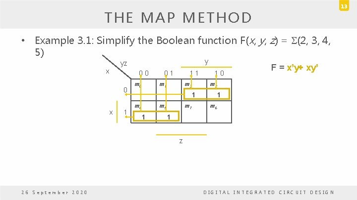
13 THE MAP METHOD • Example 3. 1: Simplify the Boolean function F(x, y, z) = S(2, 3, 4, 5) y yz x 0 0 0 x 1 m 0 0 1 1 1 m 3 1 0 m 2 1 m 4 m 5 1 m 7 F = x’y+ xy’ 1 m 6 1 z 26 September 2020 DIGITAL INTEGRATED CIRCUIT DESIGN

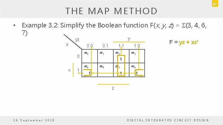
14 THE MAP METHOD • Example 3. 2: Simplify the Boolean function F(x, y, z) = S(3, 4, 6, 7) y yz x 0 0 0 x 1 m 0 0 1 1 1 m 3 1 0 F = yz + xz’ m 2 1 m 4 m 5 m 7 1 m 6 1 1 z 26 September 2020 DIGITAL INTEGRATED CIRCUIT DESIGN

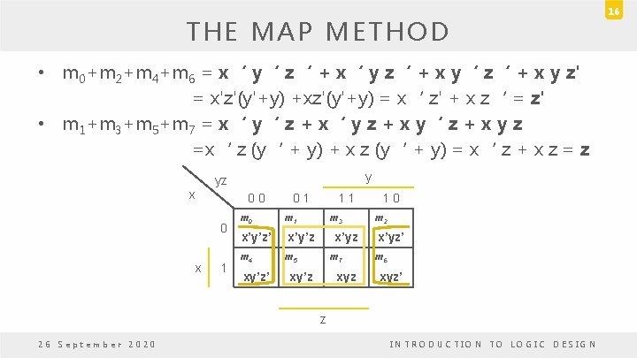
THE MAP METHOD • Consider four adjacent squares in the three-variable map. • Any such combination represents the logical sum of four minterms and results in an expression of only one literal. • The number of adjacent squares that may be combined – power of two – 1, 2, 4 and 8. • Larger number of adjacent squares – Product term with fewer literal 26 September 2020 INTRODUCTION TO LOGIC DESIGN 15

THE MAP METHOD • m 0+m 2+m 4+m 6 = x‘ y‘ z‘ + x‘ y z‘ + x y‘ z‘ + x y z' = x'z'(y'+y) +xz'(y'+y) = x‘ z' + x z‘ = z' • m 1+m 3+m 5+m 7 = x‘ y‘ z + x‘ y z + x y‘ z + x y z =x‘ z (y‘ + y) + x z (y‘ + y) = x‘ z + x z = z y yz x 0 0 0 x 1 0 1 m 0 m 1 x’y’z’ x’y’z m 4 m 5 xy’z’ 1 1 m 3 x’yz m 7 xy’z xyz 1 0 m 2 x’yz’ m 6 xyz’ z 26 September 2020 INTRODUCTION TO LOGIC DESIGN 16

THE MAP METHOD • 1 square represents 1 minterm – A Term of 3 literals. • 2 adjacent squares – A term of 2 literals. • 4 adjacent squares – A term of 1 literal. • 8 adjacent squares – Entire map – Function F = 1 26 September 2020 INTRODUCTION TO LOGIC DESIGN 17

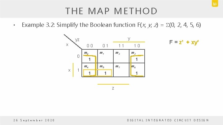
18 THE MAP METHOD • Example 3. 2: Simplify the Boolean function F(x, y, z) = S(0, 2, 4, 5, 6) y yz x 0 0 0 x 1 m 0 0 1 1 1 m 3 1 0 m 2 1 m 4 1 m 5 1 F = z’ + xy’ m 7 1 m 6 1 z 26 September 2020 DIGITAL INTEGRATED CIRCUIT DESIGN

THE MAP METHOD • If a funtion is not expressed in sum of minterms – Use the map to obtain the minterms – Simplify the function and find the minimum number of terms. – Make sure that the algebraic expression is in sum of products form. 26 September 2020 INTRODUCTION TO LOGIC DESIGN 19

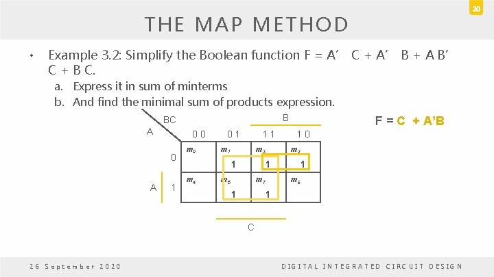
20 THE MAP METHOD • Example 3. 2: Simplify the Boolean function F = A’ C + A’ B + A B’ C + B C. a. Express it in sum of minterms b. And find the minimal sum of products expression. B BC A 0 0 0 A 1 m 0 0 1 1 1 m 3 1 m 4 F = C + A’B 1 0 m 2 1 m 5 m 7 1 1 m 6 1 C 26 September 2020 DIGITAL INTEGRATED CIRCUIT DESIGN

3. 2 FOUR – VARIABLE K-MAP

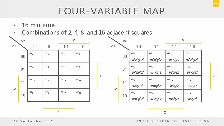
22 FOUR-VARIABLE MAP • • 16 minterms Combinations of 2, 4, 8, and 16 adjacent squares y yz wx 0 0 00 01 11 w 10 m 4 m 12 m 8 0 1 1 1 m 3 m 5 m 7 m 13 m 15 m 9 m 11 z 26 September 2020 y yz wx 1 0 m 2 00 m 6 m 14 m 10 0 0 01 x 11 w 10 0 1 m 0 m 1 w’x’y’z’ w’x’y’z m 4 m 5 w’xy’z’ m 12 1 1 m 3 w’x’yz m 7 w’xy’z w’xyz m 13 wxy’z’ m 8 m 15 wxy’z wxyz m 9 wx’y’z’ m 11 wx’y’z wx’yz 1 0 m 2 w’x’yz’ m 6 w’xyz’ m 14 wxyz’ m 10 wxyz’ z INTRODUCTION TO LOGIC DESIGN x

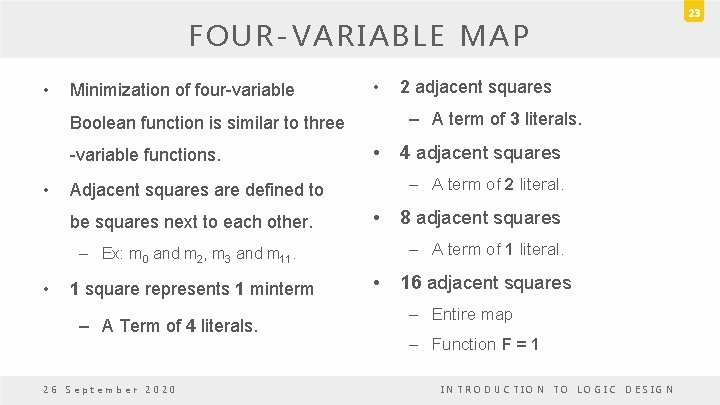
FOUR-VARIABLE MAP • Minimization of four-variable • – A term of 3 literals. Boolean function is similar to three -variable functions. • • • 1 square represents 1 minterm – A Term of 4 literals. 26 September 2020 8 adjacent squares – A term of 1 literal. – Ex: m 0 and m 2, m 3 and m 11. • 4 adjacent squares – A term of 2 literal. Adjacent squares are defined to be squares next to each other. 2 adjacent squares • 16 adjacent squares – Entire map – Function F = 1 INTRODUCTION TO LOGIC DESIGN 23

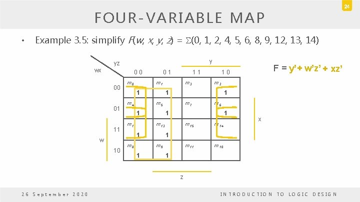
24 FOUR-VARIABLE MAP • Example 3. 5: simplify F(w, x, y, z) = S(0, 1, 2, 4, 5, 6, 8, 9, 12, 13, 14) y yz wx 0 0 00 01 11 w 10 m 0 0 1 1 1 m 4 m 3 1 m 5 m 12 m 7 1 1 m 15 m 14 m 11 m 10 x 1 m 9 1 m 6 1 m 13 m 8 m 2 1 1 F = y’+ w’z’ + xz’ 1 0 1 z 26 September 2020 INTRODUCTION TO LOGIC DESIGN

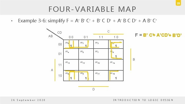
FOUR-VARIABLE MAP • 25 Example 3 -6: simplify F = A B C + B C D + A B C C CD AB 0 0 00 01 11 A 10 m 0 1 m 4 0 1 m 1 1 m 5 m 3 m 2 m 7 m 6 1 1 m 12 m 13 m 15 m 14 m 8 m 9 m 11 m 10 1 1 F = B’ C’+ A’CD’+ B’D’ 1 0 B 1 D 26 September 2020 INTRODUCTION TO LOGIC DESIGN

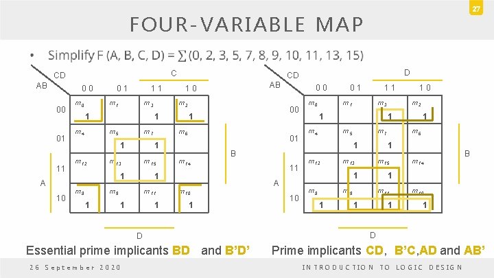
FOUR-VARIABLE MAP • Prime implicant is a product term obtained by combining the maximum possible number of adjacent squares in the map. • If a minterm in a square is covered by only one prime implicant, that prime implicant is said to be essential. 26 September 2020 INTRODUCTION TO LOGIC DESIGN 26

27 FOUR-VARIABLE MAP • C CD AB 0 0 00 01 11 A 10 m 0 0 1 1 1 m 3 1 m 4 m 12 m 13 01 m 14 B 1 m 9 1 m 6 m 15 m 11 1 1 m 10 1 D Essential prime implicants BD and B’D’ 26 September 2020 0 0 00 1 1 1 m 8 m 2 m 7 1 AB 1 0 1 m 5 D CD 11 A 10 m 0 0 1 1 1 m 3 1 m 4 m 7 1 m 13 m 6 m 15 m 14 B 1 m 9 1 1 m 8 m 2 1 m 5 m 12 1 0 m 11 1 1 m 10 1 D Prime implicants CD, B’C, AD and AB’ INTRODUCTION TO LOGIC DESIGN

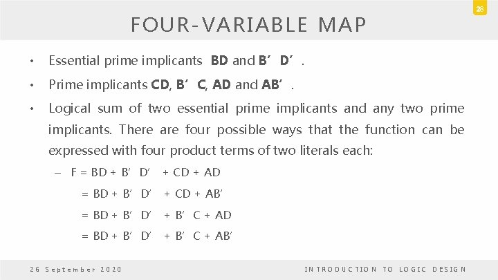
FOUR-VARIABLE MAP • Essential prime implicants BD and B’D’. • Prime implicants CD, B’C, AD and AB’. • Logical sum of two essential prime implicants and any two prime implicants. There are four possible ways that the function can be expressed with four product terms of two literals each: – F = BD + B’D’ + CD + AD = BD + B’D’ + CD + AB’ = BD + B’D’ + B’C + AD = BD + B’D’ + B’C + AB’ 26 September 2020 INTRODUCTION TO LOGIC DESIGN 28

3. 3 FIVE – VARIABLE K-MAP

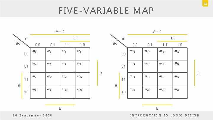
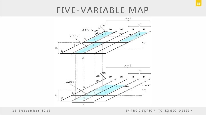
FIVE-VARIABLE MAP • Maps for more than four variables becomes complicated. • A five-variable map needs 32 squares and a six-variable map needs 64 squares. • When the number of variables becomes large, • The number of squares becomes excessively large, • The geometry for combining adjacent squares becomes more involved. • Five-variable map: two four-variable map (one on the top of the other). 26 September 2020 INTRODUCTION TO LOGIC DESIGN 30

31 FIVE-VARIABLE MAP A = 0 A = 1 D DE BC 0 0 00 01 11 B 10 0 1 1 1 m 3 m 2 m 4 m 5 m 7 m 6 m 12 m 13 m 15 m 14 m 8 m 9 m 11 m 10 26 September 2020 BC 1 0 m 0 E D DE 0 0 00 01 C 11 B 10 0 1 1 0 m 16 m 17 m 19 m 18 m 20 m 21 m 23 M 22 m 28 m 29 m 31 m 30 m 24 m 25 m 27 m 26 C E INTRODUCTION TO LOGIC DESIGN

FIVE-VARIABLE MAP • Each four-variable map retains the previously defined adjacency when taken separately. • Each square in the A = 0 map is a adjacent to the corresponding square in the A = 1. – Ex: m 4 is adjacent to m 20 and m 15 to m 31. • For six-variable map 4 x four-variable maps needed to obtain the required 64 squares. • Variables > 6 need to many squares and are impractical to use. 26 September 2020 INTRODUCTION TO LOGIC DESIGN 32

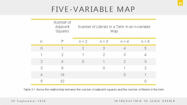
33 FIVE-VARIABLE MAP Number of Adjacent Squares Number of Literals in a Term in an n-variable Map K 2 k n = 2 n = 3 n = 4 n = 5 0 1 2 3 4 5 1 2 3 4 2 4 0 1 2 3 3 8 0 1 2 4 16 0 1 5 32 0 Table 3. 1 shows the relationship between the number of adjacent squares and the number of literals in the term. 26 September 2020 INTRODUCTION TO LOGIC DESIGN

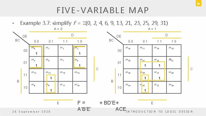
34 FIVE-VARIABLE MAP Example 3. 7: simplify F = S(0, 2, 4, 6, 9, 13, 21, 23, 25, 29, 31) • A = 0 A = 1 D DE BC 0 0 00 01 11 B 10 m 0 0 1 1 1 m 3 m 2 m 7 1 m 6 1 m 13 m 15 m 14 1 m 8 m 9 m 11 m 10 1 E 26 September 2020 F = A’B’E’ 0 0 00 1 m 5 m 12 BC 1 0 1 m 4 D DE 01 C 11 B 10 0 1 1 0 m 16 m 17 m 19 m 18 m 20 m 21 m 23 M 22 1 m 28 m 29 1 m 24 m 25 1 m 30 C 1 m 27 m 26 1 E + BD’E + ACE I N T R O D U C T I O N T O L O G I C D E S I G N

FIVE-VARIABLE MAP 26 September 2020 INTRODUCTION TO LOGIC DESIGN 35

3. 4 PRODUCT OF SUMS SIMPLIFICATION

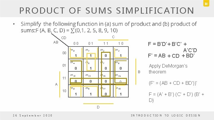
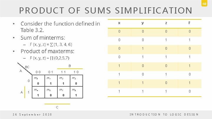
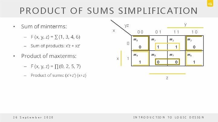
PRODUCT OF SUMS SIMPLIFICATION • The 1’s placed in the squares of the map represent the minterms of the function. • The minterms not included in the function denote the complement of the function. • Mark the empty squares by 0’s • Combine them into valid adjacent squares • Obtain simplified expression of the complement function F’. 26 September 2020 INTRODUCTION TO LOGIC DESIGN 37

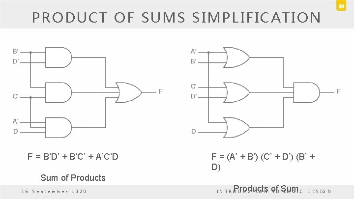
PRODUCT OF SUMS SIMPLIFICATION 38 • C CD AB 0 0 00 01 11 A 10 m 0 0 1 1 1 m 4 m 3 1 0 m 12 m 8 m 7 1 m 15 0 0 m 9 1 m 11 1 1 m 6 0 m 13 0 m 2 0 m 5 F = B’D’ + B’C’ + A’C’D F’ = AB + CD + BD’ 1 0 0 0 m 14 0 B Apply De. Morgan’s theorem (F’ = (AB + CD + BD’))’ m 10 1 F = (A’ + B’) (C’ + D’) (B’ + D) D 26 September 2020 INTRODUCTION TO LOGIC DESIGN

PRODUCT OF SUMS SIMPLIFICATION F = B’D’ + B’C’ + A’C’D Sum of Products 26 September 2020 F = (A’ + B’) (C’ + D’) (B’ + D) Products of Sum INTRO DUCTION TO LOGIC DESIGN 39

PRODUCT OF SUMS SIMPLIFICATION • B BC A 0 0 0 A 1 m 0 0 m 4 1 0 1 1 1 m 3 1 1 m 5 m 7 0 0 1 0 m 2 0 m 6 x y z F 0 0 0 1 1 0 0 1 1 1 1 0 1 C 26 September 2020 INTRODUCTION TO LOGIC DESIGN 40

PRODUCT OF SUMS SIMPLIFICATION • y yz x 0 0 0 x 1 m 0 0 1 1 1 m 1 0 m 4 m 3 1 m 2 1 m 5 1 1 0 m 7 0 0 m 6 0 1 z 26 September 2020 INTRODUCTION TO LOGIC DESIGN 41

3. 5 DON’T CARE CONDITIONS

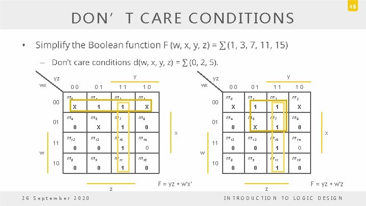
DON’T CARE CONDITIONS • The value of a function is not specified for certain combinations of variables – BCD; 1010 -1111: don't care • These don’t care conditions can be used on a map to provide further simplification of the Boolean expression. • Don’t care minterm is a combination of variables whole logical value is not specified. 26 September 2020 INTRODUCTION TO LOGIC DESIGN 43

DON’T CARE CONDITIONS • It cannot be marked with a 1 in the map – It would require that the function always be a 1 for such combination. • It cannot be marked with a 0 in the map – It would require that the function always be a 0 for such combination. • For don’t care conditions an X is used. • For adjacent squares in the map to simplify the function – The don’t care minterms may be assumed to be either 0 or 1. 26 September 2020 INTRODUCTION TO LOGIC DESIGN 44

45 DON’T CARE CONDITIONS • y yz wx 0 0 00 01 11 w 10 m 0 0 1 1 1 m 1 X m 4 m 3 1 0 m 12 m 8 m 15 0 1 m 9 0 m 11 0 1 z 26 September 2020 X 0 m 14 0 0 00 m 6 1 m 13 0 m 2 m 7 X wx 1 0 1 m 5 y yz 01 x 11 0 w m 10 10 0 F = yz + w’x’ m 0 X m 4 0 1 1 1 m 3 1 1 m 5 m 7 1 0 m 2 X m 6 0 X 1 0 m 12 m 13 m 15 m 14 0 0 1 0 m 11 m 10 1 0 m 8 0 m 9 0 z x F = yz + w’z INTRODUCTION TO LOGIC DESIGN

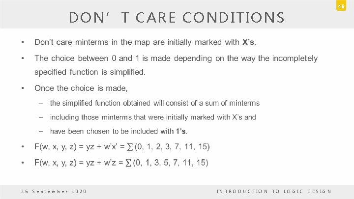
DON’T CARE CONDITIONS • 26 September 2020 INTRODUCTION TO LOGIC DESIGN 46

3. 6 NAND NOR IMPLEMENTATIONS

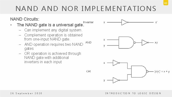
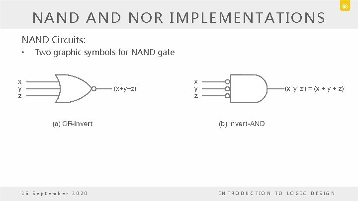
NAND NOR IMPLEMENTATIONS NAND Circuits: • The NAND gate is a universal gate. – Can implement any digital system. – Complement operation is obtained from one-input NAND gate. – AND operation requires two NAND gates – OR operation is achieved through NAND gate with additional inverters in each input 26 September 2020 INTRODUCTION TO LOGIC DESIGN 48

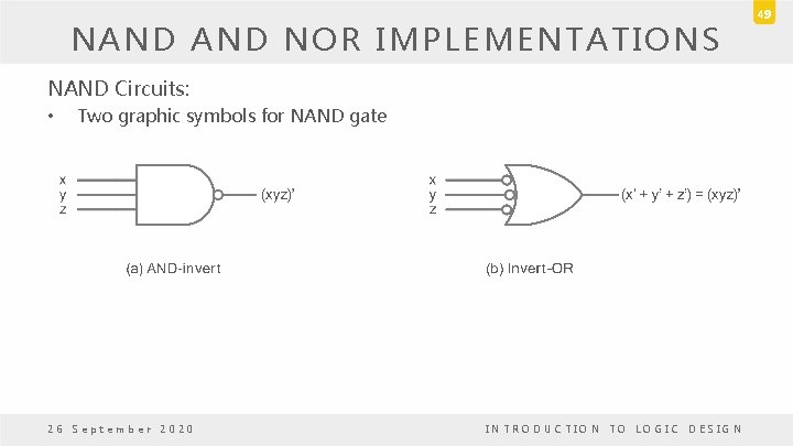
NAND NOR IMPLEMENTATIONS NAND Circuits: • Two graphic symbols for NAND gate 26 September 2020 INTRODUCTION TO LOGIC DESIGN 49

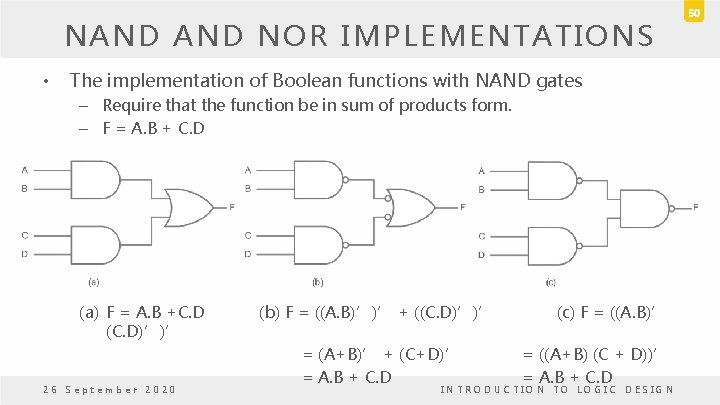
NAND NOR IMPLEMENTATIONS • The implementation of Boolean functions with NAND gates – Require that the function be in sum of products form. – F = A. B + C. D (a) F = A. B +C. D (C. D)’)’ 26 September 2020 (b) F = ((A. B)’)’ + ((C. D)’)’ (c) F = ((A. B)’ = (A+B)’ + (C+D)’ = ((A+B) (C + D))’ = A. B + C. D INTRODUCTION TO LOGIC DESIGN 50

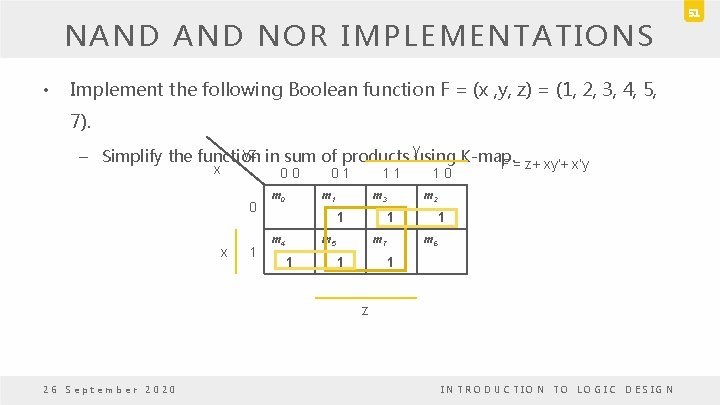
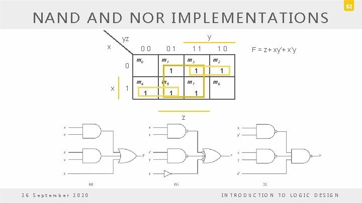
NAND NOR IMPLEMENTATIONS • Implement the following Boolean function F = (x , y, z) = (1, 2, 3, 4, 5, 7). y yz – Simplify the function in sum of products using K-map. F = z + xy’+ x’y x 0 0 0 x 1 m 0 0 1 1 1 m 3 1 m 4 m 2 1 m 5 1 1 0 m 7 1 1 m 6 1 z 26 September 2020 INTRODUCTION TO LOGIC DESIGN 51

NAND NOR IMPLEMENTATIONS y yz x 0 0 0 x 1 m 0 0 1 1 1 m 3 1 m 4 m 7 1 F = z + xy’+ x’y m 2 1 m 5 1 1 0 1 m 6 1 z 26 September 2020 INTRODUCTION TO LOGIC DESIGN 52

NAND NOR IMPLEMENTATIONS • The procedure – Simplify in the form of sum of products; – Draw a NAND gate for each product term; § The inputs to each NAND gate are the literals of the term (the first level); – A single NAND gate for the second sum term (the second level); – A term with a single literal requires an inverter in the first level if the single literal is not complemented. Otherwise it can be connected directly. 26 September 2020 INTRODUCTION TO LOGIC DESIGN 53

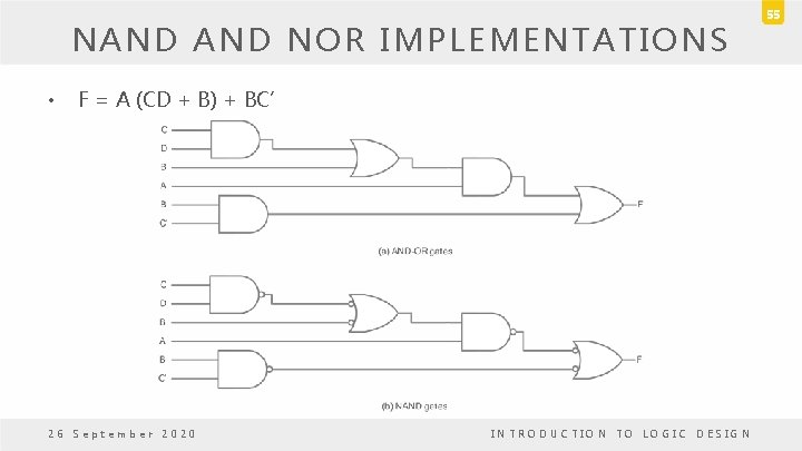
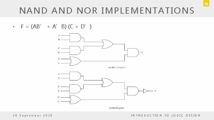
NAND NOR IMPLEMENTATIONS • General procedure for converting multilevel AND-OR diagram into all NAND diagram: – Convert all AND gates to NAND gates with AND-invert graphic symbol. – Convert all OR gates to NAND gates with invert-OR graphic symbol. – Check all the bubbles in the diagram. • For every bubble that is not compensated by another small circle along the same line, • insert an inverter (one-input NAND gate) or • complement the input literal 26 September 2020 INTRODUCTION TO LOGIC DESIGN 54

NAND NOR IMPLEMENTATIONS • F = A (CD + B) + BC’ 26 September 2020 INTRODUCTION TO LOGIC DESIGN 55

NAND NOR IMPLEMENTATIONS • F = (AB’ + A’B) (C + D’) 26 September 2020 INTRODUCTION TO LOGIC DESIGN 56

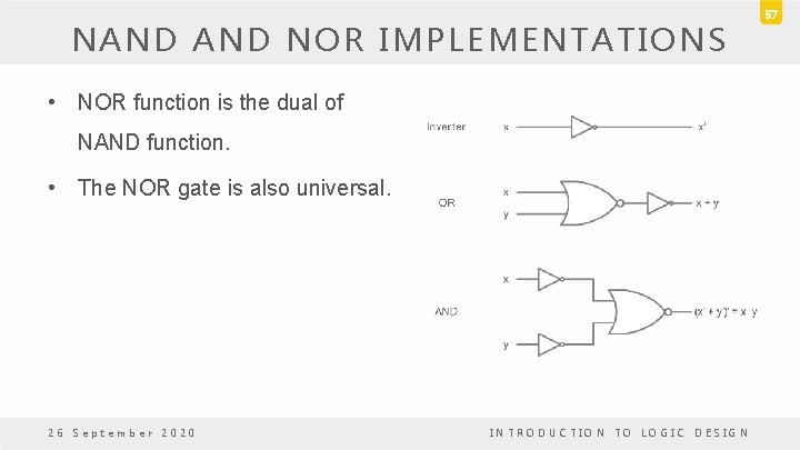
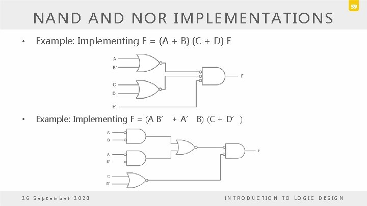
NAND NOR IMPLEMENTATIONS • NOR function is the dual of NAND function. • The NOR gate is also universal. 26 September 2020 INTRODUCTION TO LOGIC DESIGN 57

NAND NOR IMPLEMENTATIONS NAND Circuits: • Two graphic symbols for NAND gate 26 September 2020 INTRODUCTION TO LOGIC DESIGN 58

NAND NOR IMPLEMENTATIONS • Example: Implementing F = (A + B) (C + D) E • Example: Implementing F = (A B’ + A’ B) (C + D’) 26 September 2020 INTRODUCTION TO LOGIC DESIGN 59

3. 7 OTHER TWO LEVEL IMPLEMENTATIONS

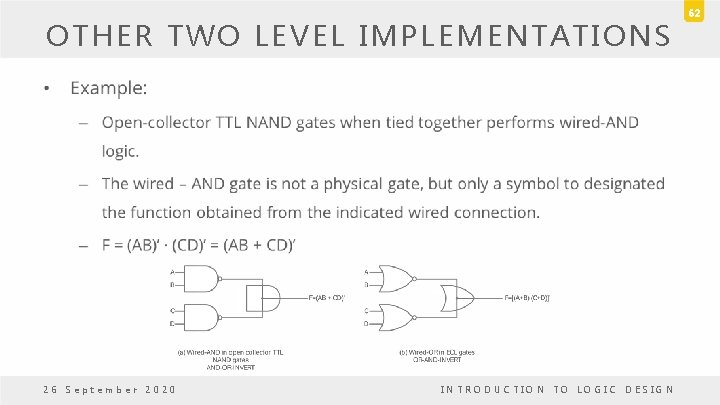
OTHER TWO LEVEL IMPLEMENTATIONS • NAND and NOR gates most often found in integrated circuits. • NAND and NOR are the most important gates from a practical point of view. • Some NAND or NOR gates allow the possibility of a wire connection between the outputs of two gates to provide a specific logic function. • This type of logic is called wired logic. • Example: – Open-collector TTL NAND gates when tied together performs wired-AND logic. 26 September 2020 INTRODUCTION TO LOGIC DESIGN 61

OTHER TWO LEVEL IMPLEMENTATIONS • 26 September 2020 INTRODUCTION TO LOGIC DESIGN 62

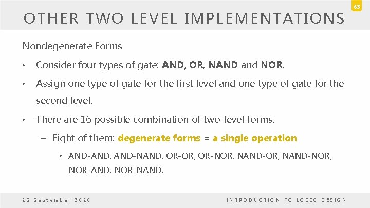
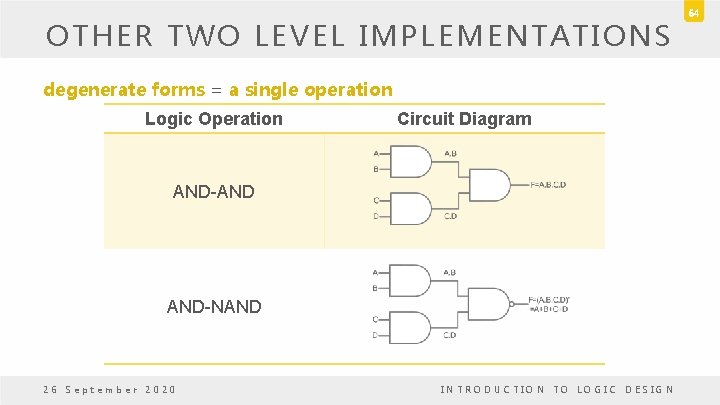
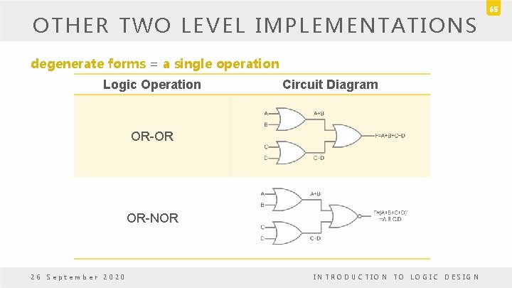
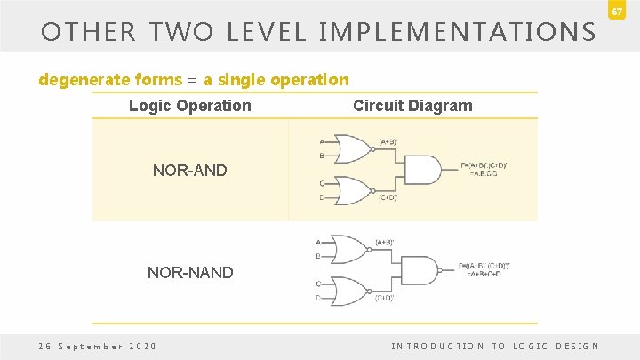
OTHER TWO LEVEL IMPLEMENTATIONS Nondegenerate Forms • Consider four types of gate: AND, OR, NAND and NOR. • Assign one type of gate for the first level and one type of gate for the second level. • There are 16 possible combination of two-level forms. – Eight of them: degenerate forms = a single operation • AND-AND, AND-NAND, OR-OR, OR-NOR, NAND-NOR, NOR-AND, NOR-NAND. 26 September 2020 INTRODUCTION TO LOGIC DESIGN 63

OTHER TWO LEVEL IMPLEMENTATIONS degenerate forms = a single operation Logic Operation Circuit Diagram AND-AND AND-NAND 26 September 2020 INTRODUCTION TO LOGIC DESIGN 64

OTHER TWO LEVEL IMPLEMENTATIONS degenerate forms = a single operation Logic Operation Circuit Diagram OR-OR OR-NOR 26 September 2020 INTRODUCTION TO LOGIC DESIGN 65

OTHER TWO LEVEL IMPLEMENTATIONS degenerate forms = a single operation Logic Operation Circuit Diagram NAND-OR NAND-NOR 26 September 2020 INTRODUCTION TO LOGIC DESIGN 66

OTHER TWO LEVEL IMPLEMENTATIONS degenerate forms = a single operation Logic Operation Circuit Diagram NOR-AND NOR-NAND 26 September 2020 INTRODUCTION TO LOGIC DESIGN 67

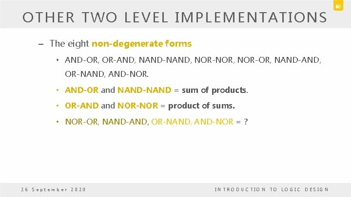
OTHER TWO LEVEL IMPLEMENTATIONS – The eight non-degenerate forms • AND-OR, OR-AND, NAND-NAND, NOR-NOR, NOR-OR, NAND-AND, OR-NAND, AND-NOR. • AND-OR and NAND-NAND = sum of products. • OR-AND and NOR-NOR = product of sums. • NOR-OR, NAND-AND, OR-NAND, AND-NOR = ? 26 September 2020 INTRODUCTION TO LOGIC DESIGN 68

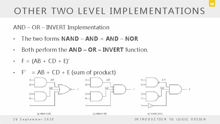
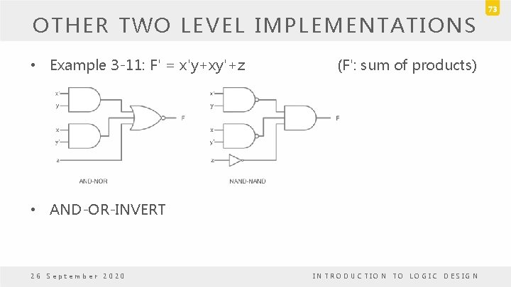
OTHER TWO LEVEL IMPLEMENTATIONS AND – OR – INVERT Implementation • The two forms NAND – AND = AND – NOR • Both perform the AND – OR – INVERT function. • F = (AB + CD + E)’ • F’ = AB + CD + E (sum of product) 26 September 2020 INTRODUCTION TO LOGIC DESIGN 69

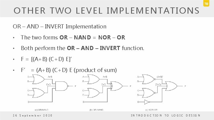
OTHER TWO LEVEL IMPLEMENTATIONS OR – AND – INVERT Implementation • The two forms OR – NAND = NOR – OR • Both perform the OR – AND – INVERT function. • F = [(A+B) (C+D) E]’ • F’ = (A+B) (C+D) E (product of sum) 26 September 2020 INTRODUCTION TO LOGIC DESIGN 70

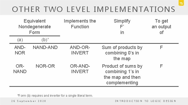
OTHER TWO LEVEL IMPLEMENTATIONS Equivalent Nondegenerate Form Implements the Function Simplify F’ in To get an output of (a) (b)* ANDNOR NAND-AND AND-ORINVERT Sum of products by combining 0’s in the map F ORNAND NOR-OR OR-ANDINVERT Product of sums by combining 1’s in the map and then complementing F *Form (b) requires and inverter for a single literal term. 26 September 2020 INTRODUCTION TO LOGIC DESIGN 71

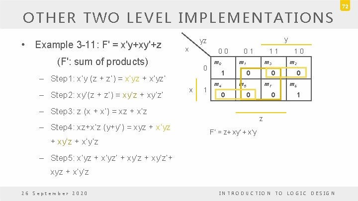
OTHER TWO LEVEL IMPLEMENTATIONS • Example 3 -11: F' = x'y+xy'+z x 0 0 (F': sum of products) 0 – Step 1: x’y (z + z’) = x’yz + x’yz’ – Step 2: xy’(z + z’) = xy’z + xy’z’ y yz x 1 m 0 0 1 m 1 1 m 4 m 3 0 0 1 0 m 2 0 m 5 m 7 0 – Step 3: z (x + x’) = xz + x’z – Step 4: xz+x’z (y+y’) = xyz + x’yz 1 1 0 m 6 0 1 z F’ = z + xy’ + x’y + xy’z + x’y’z – Step 5: x’yz + x’yz’ + xy’z’+ xyz + x’y’z 26 September 2020 INTRODUCTION TO LOGIC DESIGN 72

OTHER TWO LEVEL IMPLEMENTATIONS • Example 3 -11: F' = x'y+xy'+z (F': sum of products) • AND-OR-INVERT 26 September 2020 INTRODUCTION TO LOGIC DESIGN 73

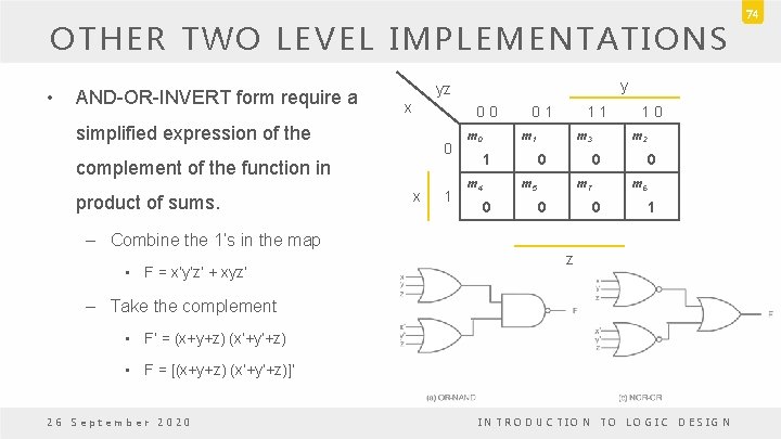
OTHER TWO LEVEL IMPLEMENTATIONS • AND-OR-INVERT form require a x 0 0 simplified expression of the 0 complement of the function in product of sums. y yz x 1 m 0 0 1 1 1 m 4 m 3 0 m 2 0 m 5 0 1 0 m 7 0 0 m 6 0 1 – Combine the 1’s in the map • F = x’y’z’ + xyz’ z – Take the complement • F’ = (x+y+z) (x’+y’+z) • F = [(x+y+z) (x’+y’+z)]’ 26 September 2020 INTRODUCTION TO LOGIC DESIGN 74

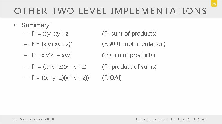
OTHER TWO LEVEL IMPLEMENTATIONS • Summary – F' = x'y+xy'+z (F': sum of products) – F = (x'y+xy'+z)' (F: AOI implementation) – F = x'y'z' + xyz' (F: sum of products) – F' = (x+y+z)(x'+y'+z) (F': product of sums) – F = ((x+y+z)(x'+y'+z))' (F: OAI) 26 September 2020 INTRODUCTION TO LOGIC DESIGN 75

3. 8 EXCLUSIVE-OR FUNCTION

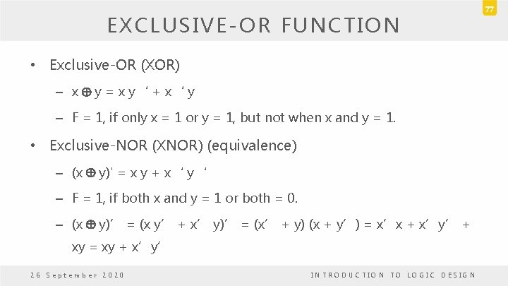
EXCLUSIVE-OR FUNCTION • Exclusive-OR (XOR) – x Å y = x y‘ + x‘ y – F = 1, if only x = 1 or y = 1, but not when x and y = 1. • Exclusive-NOR (XNOR) (equivalence) – (x Å y)' = x y + x‘ y‘ – F = 1, if both x and y = 1 or both = 0. – (x Å y)’ = (x y’ + x’ y)’ = (x’ + y) (x + y’) = x’x + x’y’ + xy = xy + x’y’ 26 September 2020 INTRODUCTION TO LOGIC DESIGN 77

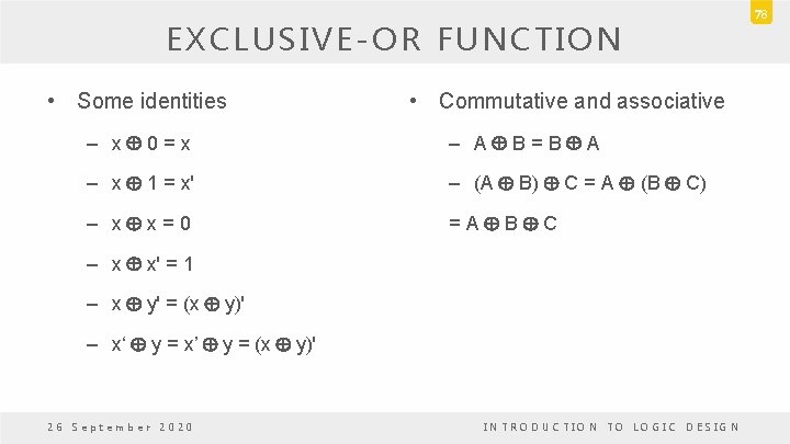
EXCLUSIVE-OR FUNCTION • Some identities • Commutative and associative – x Å 0 = x – A Å B = B Å A – x Å 1 = x' – (A Å B) Å C = A Å (B Å C) – x Å x = 0 = A Å B Å C – x Å x' = 1 – x Å y' = (x Å y)' – x‘ Å y = x’ Å y = (x Å y)' 26 September 2020 INTRODUCTION TO LOGIC DESIGN 78

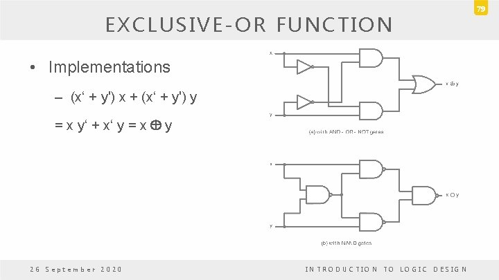
EXCLUSIVE-OR FUNCTION • Implementations – (x‘ + y') x + (x‘ + y') y = x y‘ + x‘ y = x Å y 26 September 2020 INTRODUCTION TO LOGIC DESIGN 79

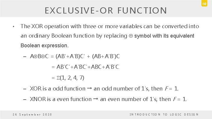
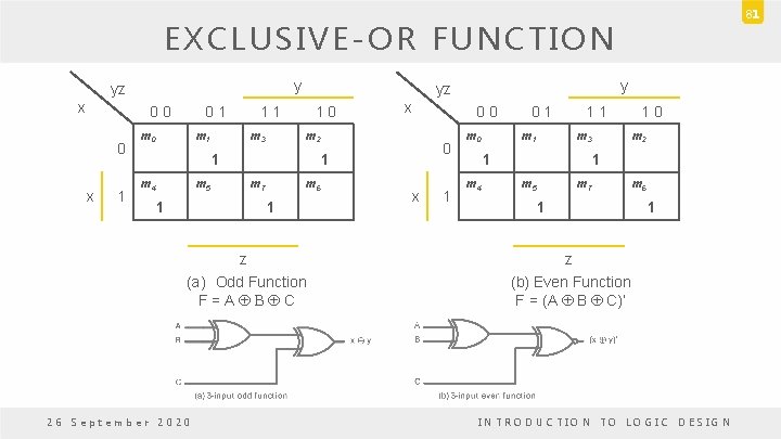
EXCLUSIVE-OR FUNCTION • The XOR operation with three or more variables can be converted into an ordinary Boolean function by replacing Å symbol with its equivalent Boolean expression. – AÅBÅC = (AB'+A'B)C' + (AB+A'B')C = AB'C'+A'BC'+ABC+A'B'C = S(1, 2, 4, 7) – XOR is a odd function → an odd number of 1's, then F = 1. – XNOR is a even function → an even number of 1's, then F = 1. 26 September 2020 INTRODUCTION TO LOGIC DESIGN 80

81 EXCLUSIVE-OR FUNCTION y yz x 0 0 0 x 1 0 1 m 0 m 1 1 1 m 3 1 0 m 5 1 0 0 0 1 m 7 m 6 1 z (a) Odd Function F = A Å B Å C 26 September 2020 x m 2 1 m 4 y yz x 1 m 0 0 1 m 1 1 1 m 3 1 m 4 1 0 m 2 1 m 5 m 7 1 m 6 1 z (b) Even Function F = (A Å B Å C)’ INTRODUCTION TO LOGIC DESIGN

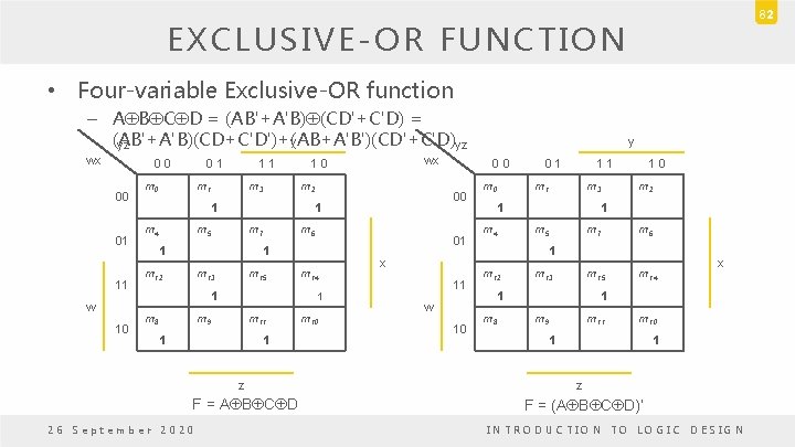
82 EXCLUSIVE-OR FUNCTION • Four-variable Exclusive-OR function – AÅBÅCÅD = (AB'+A'B)Å(CD'+C'D) = y (AB'+A'B)(CD+C'D')+(AB+A'B')(CD'+C'D) yz yz wx 0 0 00 01 11 w 10 0 1 m 0 1 1 m 3 m 2 1 m 4 m 7 1 m 6 01 1 m 13 m 15 1 m 8 m 11 1 1 z F = AÅBÅCÅD 26 September 2020 m 14 1 m 9 0 0 00 1 m 5 m 12 wx 1 0 m 10 y x 11 w 10 m 0 0 1 1 1 m 3 1 m 4 1 0 m 2 1 m 5 m 7 m 6 m 15 m 14 1 m 12 m 13 1 m 8 x 1 m 9 m 11 m 10 1 1 z F = (AÅBÅCÅD)’ INTRODUCTION TO LOGIC DESIGN

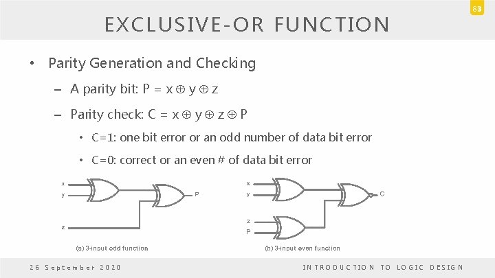
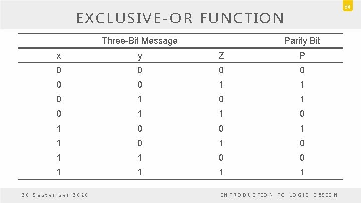
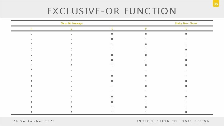
EXCLUSIVE-OR FUNCTION • Parity Generation and Checking – A parity bit: P = x Å y Å z – Parity check: C = x Å y Å z Å P • C=1: one bit error or an odd number of data bit error • C=0: correct or an even # of data bit error 26 September 2020 INTRODUCTION TO LOGIC DESIGN 83

84 EXCLUSIVE-OR FUNCTION Three-Bit Message Parity Bit x y Z P 0 0 0 1 1 0 1 0 1 0 0 1 1 0 0 1 1 26 September 2020 INTRODUCTION TO LOGIC DESIGN

85 EXCLUSIVE-OR FUNCTION Three-Bit Message Parity Error Check x y Z P C 0 0 0 0 1 1 0 0 1 0 1 0 0 1 1 0 0 0 1 1 0 0 1 0 1 0 1 1 1 0 0 0 1 1 1 1 1 0 26 September 2020 INTRODUCTION TO LOGIC DESIGN

3. 9 HARDWARE DESCRIPTION LANGUAGE

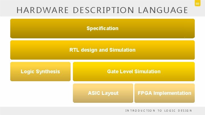
HARDWARE DESCRIPTION LANGUAGE • Describe the design of digital systems in a textual form – Hardware structure – Function/behavior – Timing • VHDL and Verilog HDL 26 September 2020 INTRODUCTION TO LOGIC DESIGN 87

HARDWARE DESCRIPTION LANGUAGE Specification RTL design and Simulation Logic Synthesis Gate Level Simulation ASIC Layout FPGA Implementation INTRODUCTION TO LOGIC DESIGN 88

HARDWARE DESCRIPTION LANGUAGE • Documentation language • HDL is used to represent and document digital systems in a form that can be read by both humans and computers • Examples of keywords: – module, end-module, input, output, wire, and, or, and not 26 September 2020 INTRODUCTION TO LOGIC DESIGN 89

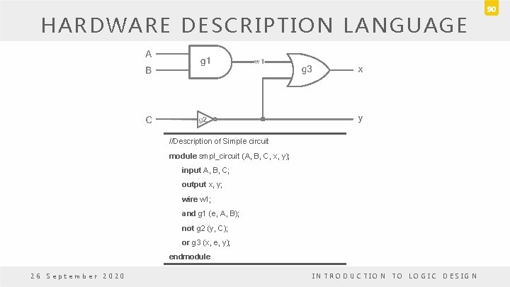
HARDWARE DESCRIPTION LANGUAGE //Description of Simple circuit module smpl_circuit (A, B, C, x, y); input A, B, C; output x, y; wire w 1; and g 1 (e, A, B); not g 2 (y, C); or g 3 (x, e, y); endmodule 26 September 2020 INTRODUCTION TO LOGIC DESIGN 90

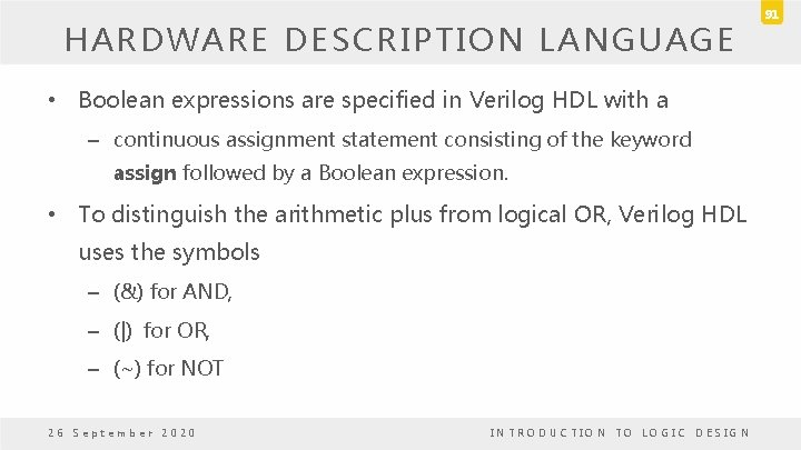
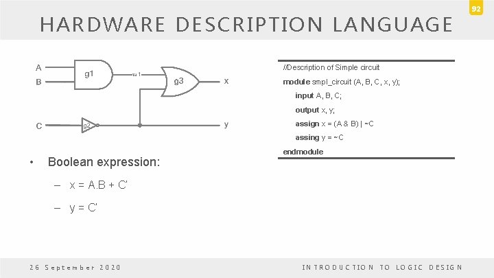
HARDWARE DESCRIPTION LANGUAGE • Boolean expressions are specified in Verilog HDL with a – continuous assignment statement consisting of the keyword assign followed by a Boolean expression. • To distinguish the arithmetic plus from logical OR, Verilog HDL uses the symbols – (&) for AND, – (|) for OR, – (~) for NOT 26 September 2020 INTRODUCTION TO LOGIC DESIGN 91

HARDWARE DESCRIPTION LANGUAGE //Description of Simple circuit module smpl_circuit (A, B, C, x, y); input A, B, C; output x, y; assign x = (A & B) | ~C assing y = ~C • Boolean expression: endmodule – x = A. B + C’ – y = C’ 26 September 2020 INTRODUCTION TO LOGIC DESIGN 92