Introduction to FPGA HIGH SPEED IO Microsoft has


- Slides: 30

Introduction to FPGA HIGH SPEED IO

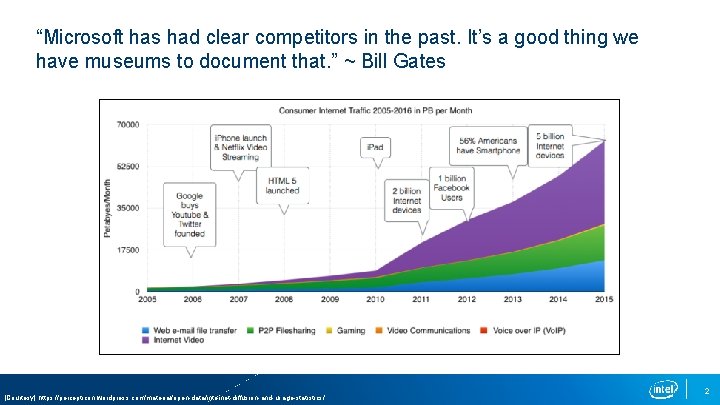
“Microsoft has had clear competitors in the past. It’s a good thing we have museums to document that. ” ~ Bill Gates [Courtesy] https: //percepticon. wordpress. com/material/open-data/internet-diffusion-and-usage-statistics/ 2

Objective of this Seminar High Speed I/O Problem Statement Vocabulary Techniques Design Flow with Intel FPGAs Hands on Lab 3

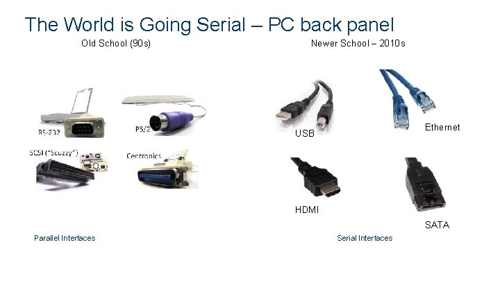
The World is Going Serial – PC back panel Old School (90 s) Newer School – 2010 s Ethernet USB HDMI SATA Parallel Interfaces Serial Interfaces 4

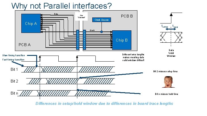
Why not Parallel interfaces? Data PCB B The “Channel” Clock Source Chip A PCB A Slow timing transition Fast timing transition Bit 1 tsetup C o n n e c t o r thold Clock Chip B Different wire lengths makes meeting data valid window difficult Data Valid Window Bit 2 misses setup time Bit 2 Bit n misses hold time Differences in setup/hold window due to differences in board trace lengths 5

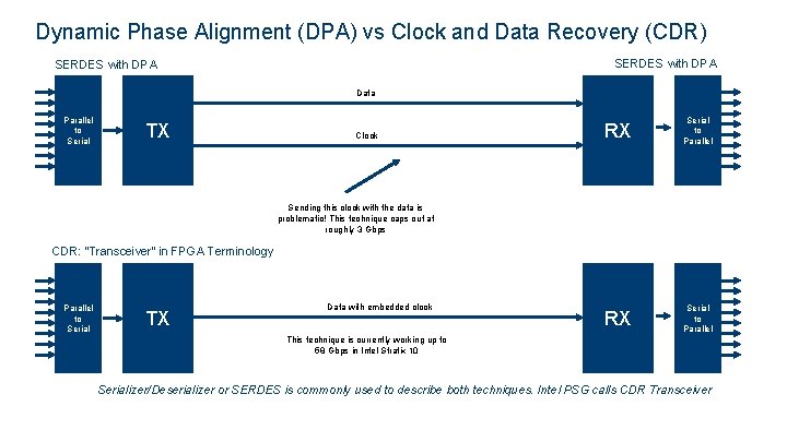
Dynamic Phase Alignment (DPA) vs Clock and Data Recovery (CDR) SERDES with DPA Data Parallel to Serial TX Clock RX Serial to Parallel Sending this clock with the data is problematic! This technique caps out at roughly 3 Gbps CDR: “Transceiver” in FPGA Terminology Parallel to Serial TX Data with embedded clock This technique is currently working up to 58 Gbps in Intel Stratix 10 Serializer/Deserializer or SERDES is commonly used to describe both techniques. Intel PSG calls CDR Transceiver 6

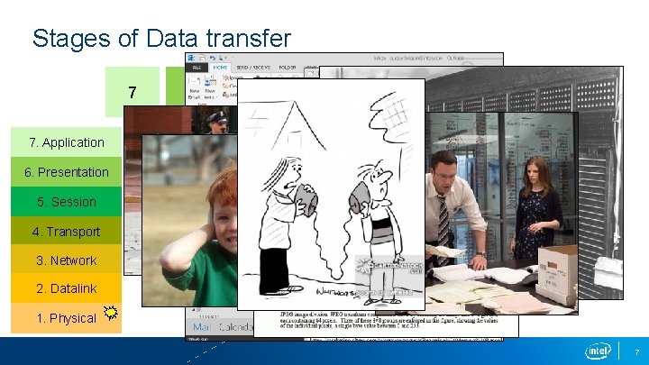
Stages of Data transfer 7 6 5 4 3 2 1 7. Application 6. Presentation 5. Session 4. Transport 3. Network 2. Datalink 1. Physical 7

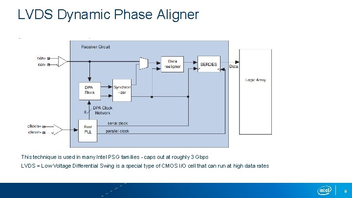
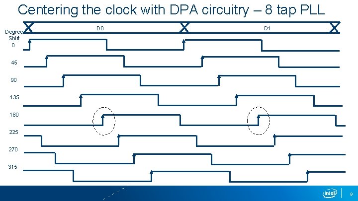
LVDS Dynamic Phase Aligner This technique is used in many Intel PSG families - caps out at roughly 3 Gbps LVDS = Low Voltage Differential Swing is a special type of CMOS I/O cell that can run at high data rates 8

Centering the clock with DPA circuitry – 8 tap PLL Degree Shift 0 D 1 45 90 135 180 225 270 315 9

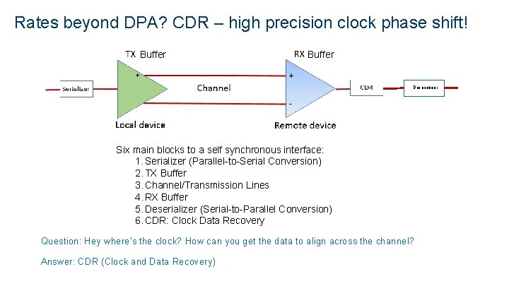
Rates beyond DPA? CDR – high precision clock phase shift! Buffer Deserializer Six main blocks to a self synchronous interface: 1. Serializer (Parallel-to-Serial Conversion) 2. TX Buffer 3. Channel/Transmission Lines 4. RX Buffer 5. Deserializer (Serial-to-Parallel Conversion) 6. CDR: Clock Data Recovery Question: Hey where’s the clock? How can you get the data to align across the channel? Answer: CDR (Clock and Data Recovery) 10

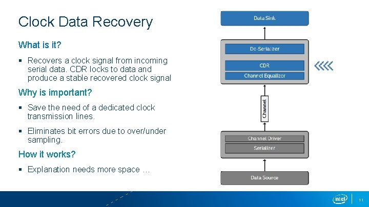
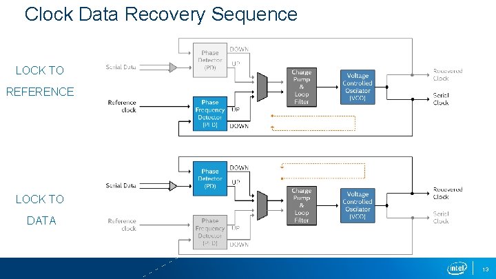
Clock Data Recovery What is it? § Recovers a clock signal from incoming serial data. CDR locks to data and produce a stable recovered clock signal Why is important? § Save the need of a dedicated clock transmission lines. § Eliminates bit errors due to over/under sampling. How it works? § Explanation needs more space … 11

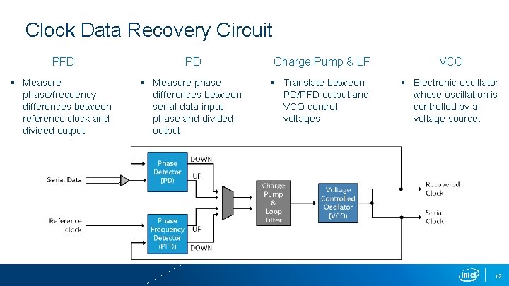
Clock Data Recovery Circuit PFD PD Charge Pump & LF VCO § Measure phase/frequency differences between reference clock and divided output. § Measure phase differences between serial data input phase and divided output. § Translate between PD/PFD output and VCO control voltages. § Electronic oscillator whose oscillation is controlled by a voltage source. 12

Clock Data Recovery Sequence LOCK TO REFERENCE LOCK TO DATA 13

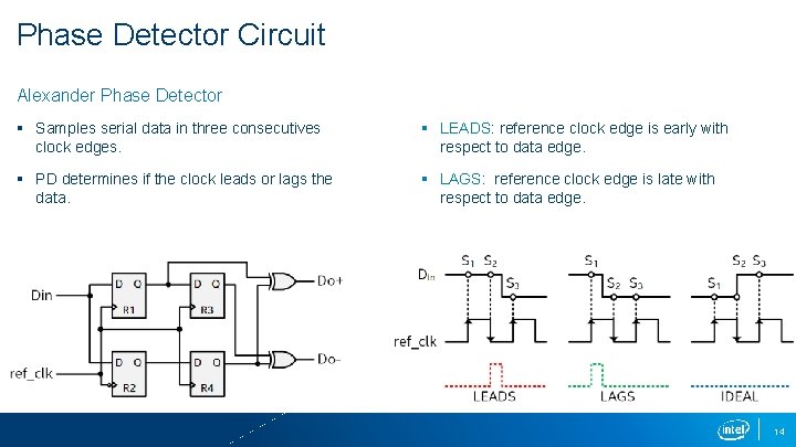
Phase Detector Circuit Alexander Phase Detector § Samples serial data in three consecutives clock edges. § LEADS: reference clock edge is early with respect to data edge. § PD determines if the clock leads or lags the data. § LAGS: reference clock edge is late with respect to data edge. 14

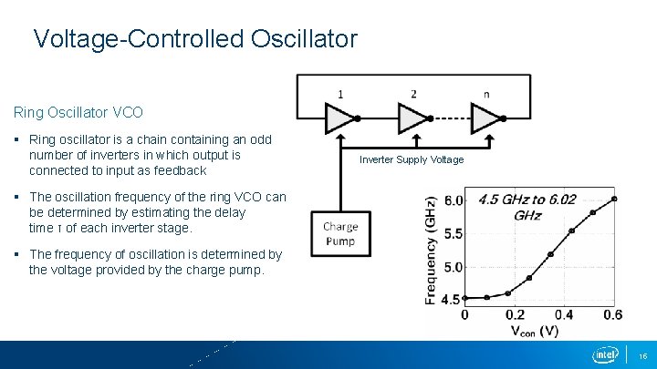
Voltage-Controlled Oscillator Ring Oscillator VCO § Ring oscillator is a chain containing an odd number of inverters in which output is connected to input as feedback Inverter Supply Voltage § The oscillation frequency of the ring VCO can be determined by estimating the delay time τ of each inverter stage. § The frequency of oscillation is determined by the voltage provided by the charge pump. 15

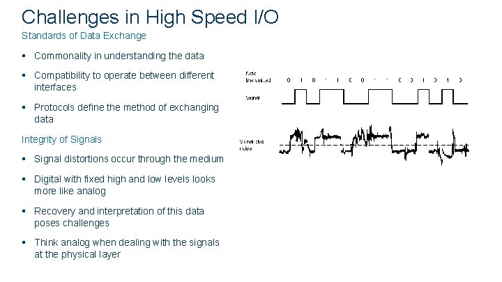
Challenges in High Speed I/O Standards of Data Exchange § Commonality in understanding the data § Compatibility to operate between different interfaces § Protocols define the method of exchanging data Integrity of Signals § Signal distortions occur through the medium § Digital with fixed high and low levels looks more like analog § Recovery and interpretation of this data poses challenges § Think analog when dealing with the signals at the physical layer 16

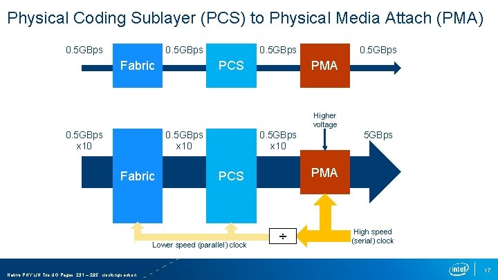
Physical Coding Sublayer (PCS) to Physical Media Attach (PMA) 0. 5 GBps Fabric 0. 5 GBps PCS PMA Higher voltage 0. 5 GBps x 10 Fabric PMA PCS Lower speed (parallel) clock Native PHY L/H Tile UG Pages: 231 – 295 : clocking section 5 GBps 0. 5 GBps x 10 ÷ High speed (serial) clock 17

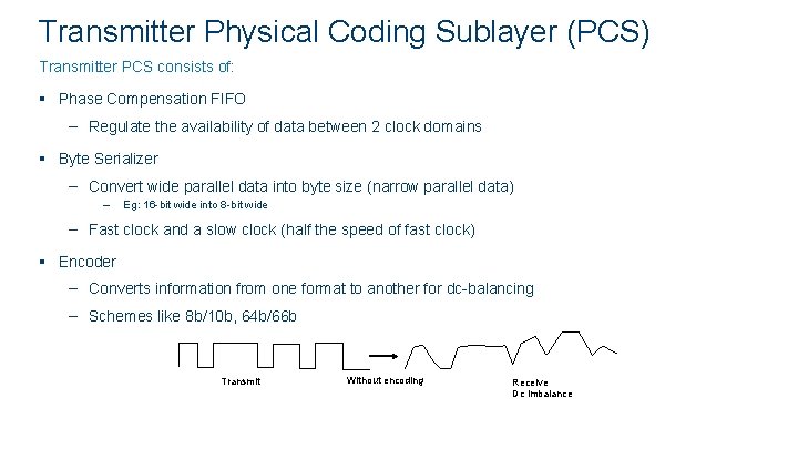
Transmitter Physical Coding Sublayer (PCS) Transmitter PCS consists of: § Phase Compensation FIFO – Regulate the availability of data between 2 clock domains § Byte Serializer – Convert wide parallel data into byte size (narrow parallel data) – Eg: 16 -bit wide into 8 -bit wide – Fast clock and a slow clock (half the speed of fast clock) § Encoder – Converts information from one format to another for dc-balancing – Schemes like 8 b/10 b, 64 b/66 b Transmit Without encoding Receive Dc imbalance 18

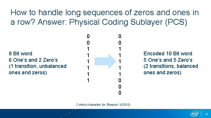
How to handle long sequences of zeros and ones in a row? Answer: Physical Coding Sublayer (PCS) 8 Bit word 6 One’s and 2 Zero’s (1 transition, unbalanced ones and zeros) 0 0 1 1 1 0 0 0 Encoded 10 Bit word 5 One’s and 5 Zero’s (2 transitions, balanced ones and zeros) Control character for ‘Beacon’ (K 28. 8) 19

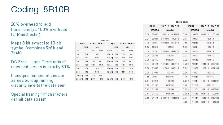
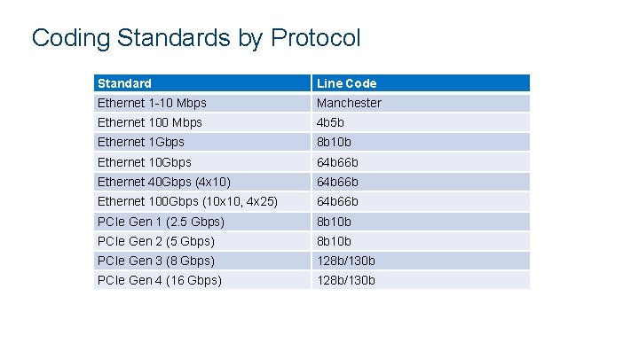
Coding: 8 B 10 B 20% overhead to add transitions (vs 100% overhead for Manchester) Maps 8 bit symbol to 10 bit symbol (combines 5 b 6 b and 3 b 4 b) DC Free – Long Term ratio of ones and zeroes is exactly 50% If unequal number of ones or zeroes buildup running disparity inverts the data sent Special framing “K” characters delimit data stream 20

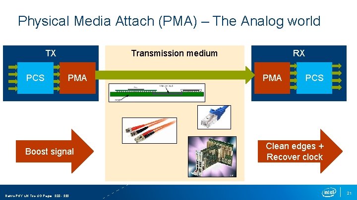
Physical Media Attach (PMA) – The Analog world Transmission medium TX PCS PMA Boost signal Native PHY L/H Tile UG Pages: 320 - 333 RX PMA PCS Clean edges + Recover clock 21

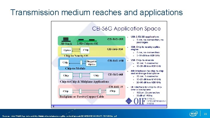
Transmission medium reaches and applications Sources: Intel PAM 4 App note and http: //www. ethernetalliance. org/wp-content/uploads/2014/10/41014 -DRAFT-TEF-56 Gbs. pdf 22

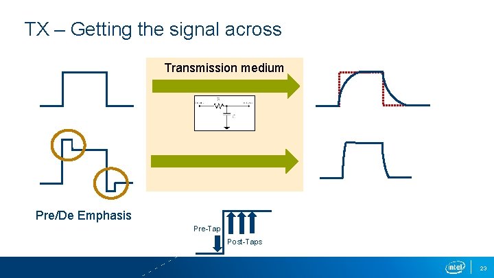
TX – Getting the signal across Transmission medium Pre/De Emphasis Pre-Tap Post-Taps 23

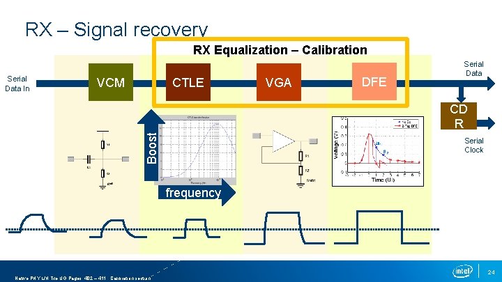
RX – Signal recovery RX Equalization – Calibration Serial Data In VCM CTLE VGA DFE Serial Data Boost CD R Serial Clock frequency 24 Native PHY L/H Tile UG Pages: 402 – 411 : Calibration section

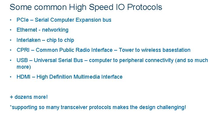
Some common High Speed IO Protocols • PCIe – Serial Computer Expansion bus • Ethernet - networking • Interlaken – chip to chip • CPRI – Common Public Radio Interface – Tower to wireless basestation • USB – Universal Serial Bus – computer to peripheral connectivity (and so much more) • HDMI – High Definition Multimedia Interface + dozens more! *supporting so many transceiver protocols makes the design challenging! 25

Coding Standards by Protocol Standard Line Code Ethernet 1 -10 Mbps Manchester Ethernet 100 Mbps 4 b 5 b Ethernet 1 Gbps 8 b 10 b Ethernet 10 Gbps 64 b 66 b Ethernet 40 Gbps (4 x 10) 64 b 66 b Ethernet 100 Gbps (10 x 10, 4 x 25) 64 b 66 b PCIe Gen 1 (2. 5 Gbps) 8 b 10 b PCIe Gen 2 (5 Gbps) 8 b 10 b PCIe Gen 3 (8 Gbps) 128 b/130 b PCIe Gen 4 (16 Gbps) 128 b/130 b 26

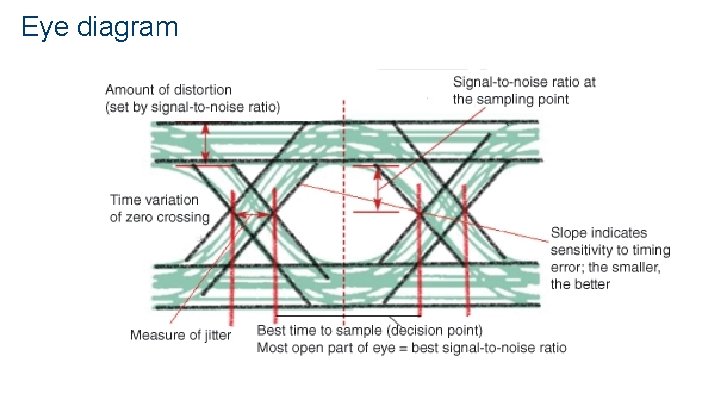
Eye diagram 27

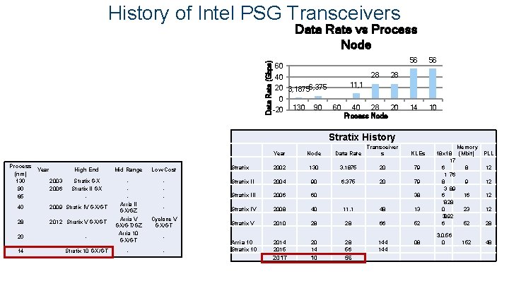
History of Intel PSG Transceivers Data Rate (Gbps) Data Rate vs Process Node 60 28 40 20 3, 18756, 375 0 60 -20 130 90 56 56 14 10 28 11, 1 40 28 20 Process Node Stratix History Process Year (nm) 130 2003 90 2006 65 High End Mid Range Low Cost Stratix GX Stratix II GX - Arria II GX/GZ Arria V GX/GT/GZ Arria 10 GX/GT - Stratix II 2004 90 Stratix III 2006 60 - Stratix IV 2008 40 11. 1 48 13 Cyclone V GX/GT Stratix V 2010 28 28 66 52 Memory 18 x 18 (Mbit) PLL 17 6 8 12 1 76 8 9 12 3 89 6 16 12 1, 28 8 0 23 12 3, 92 9 6 52 28 Arria 10 Stratix 10 2014 2015 20 14 28 56 144 08 3, 0 10, 56 0 2017 10 56 40 2009 Stratix IV GX/GT 28 2012 Stratix V GX/GT 20 - 14 Stratix 10 GX/GT - - Year Node Data Rate Transceiver s KLEs Stratix 2002 130 3. 1875 20 79 6. 375 20 79 38 152 48 28

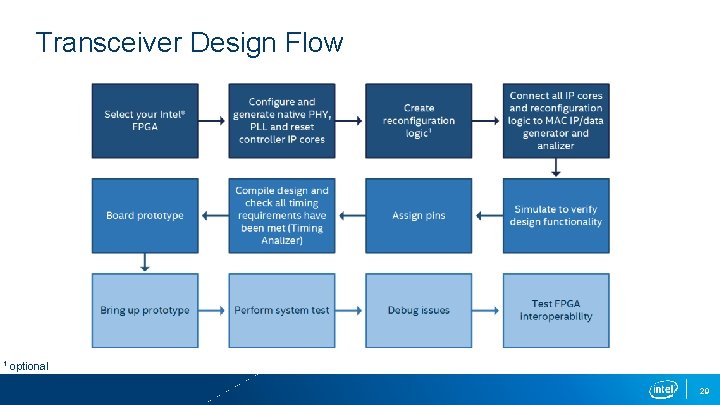
Transceiver Design Flow 1 optional 29
