Introduction to Field Programmable Gate Arrays FPGAs COE
Introduction to Field Programmable Gate Arrays (FPGAs) COE 203 Digital Logic Laboratory Dr. Aiman El-Maleh College of Computer Sciences and Engineering King Fahd University of Petroleum and Minerals
Outline v What is an FPGA v CLB Slice Structure v LUT (Look-Up Table) Functionality v Advantges of using FPGAs v FPGA Design Flow v Digilent Spartan-3 Board v FPGA Device Part Marking Introduction to FPGAs COE 203 – Digital Design Lab – KFUPM slide 2
What is an FPGA? … v A filed programmable gate array (FPGA) is a reprogrammable silicon chip. v Using prebuilt logic blocks and programmable routing resources, you can configure these chips to implement custom hardware functionality without ever having to pick up a breadboard or soldering iron. v You develop digital computing tasks in software and compile them down to a configuration file or bitstream that contains information on how the components should be wired together. Introduction to FPGAs COE 203 – Digital Design Lab – KFUPM slide 3
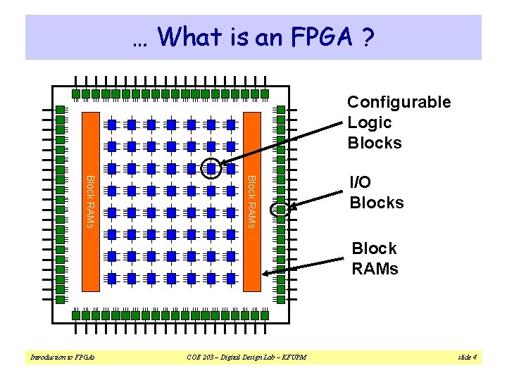
… What is an FPGA ? Configurable Logic Blocks Block RAMs I/O Blocks Block RAMs Introduction to FPGAs COE 203 – Digital Design Lab – KFUPM slide 4
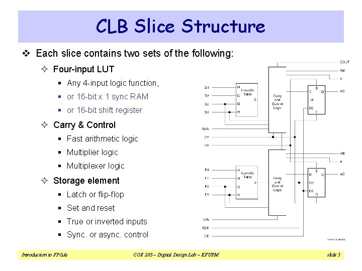
CLB Slice Structure v Each slice contains two sets of the following: ² Four-input LUT § Any 4 -input logic function, § or 16 -bit x 1 sync RAM § or 16 -bit shift register ² Carry & Control § Fast arithmetic logic § Multiplier logic § Multiplexer logic ² Storage element § Latch or flip-flop § Set and reset § True or inverted inputs § Sync. or async. control Introduction to FPGAs COE 203 – Digital Design Lab – KFUPM slide 5
LUT (Look-Up Table) Functionality • Look-Up tables are primary elements for logic implementation • Each LUT can implement any function of 4 inputs Introduction to FPGAs COE 203 – Digital Design Lab – KFUPM slide 6
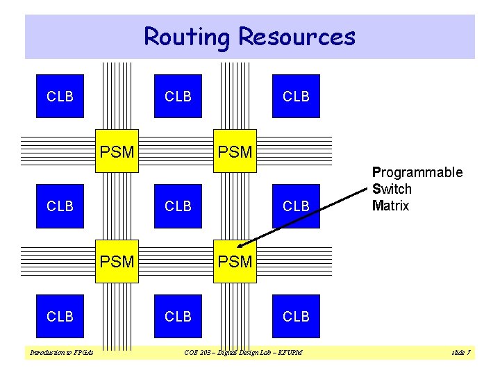
Routing Resources CLB PSM CLB Introduction to FPGAs CLB Programmable Switch Matrix PSM CLB COE 203 – Digital Design Lab – KFUPM slide 7
Advantages of using FPGAs v Creating intricate circuit designs from discrete parts, such as TTL chips, can be very tedious and error prone. v It can take a large number of chips to create a design of only moderate complexity. v It takes a lot of time to wire together a large number o f chips. Additionally, it can often be difficult to find misplaced wires when debugging a complex circuit. v Using FPGAs, it is possible to implement a complex logic design in a manner which is easy to test, debug and even change. v Using FPGAs, If the device does not function as it should, it is only necessary to debug the program as opposed to debugging the wiring of a circuit made from discrete chips. Introduction to FPGAs COE 203 – Digital Design Lab – KFUPM slide 8
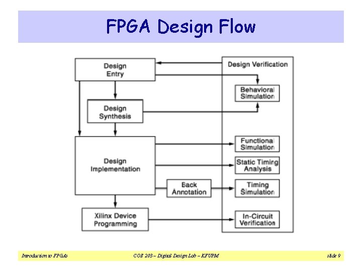
FPGA Design Flow Introduction to FPGAs COE 203 – Digital Design Lab – KFUPM slide 9
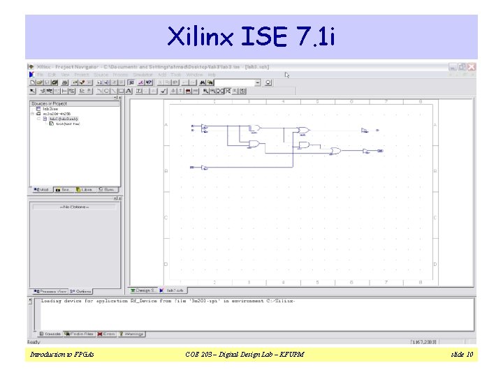
Xilinx ISE 7. 1 i Introduction to FPGAs COE 203 – Digital Design Lab – KFUPM slide 10
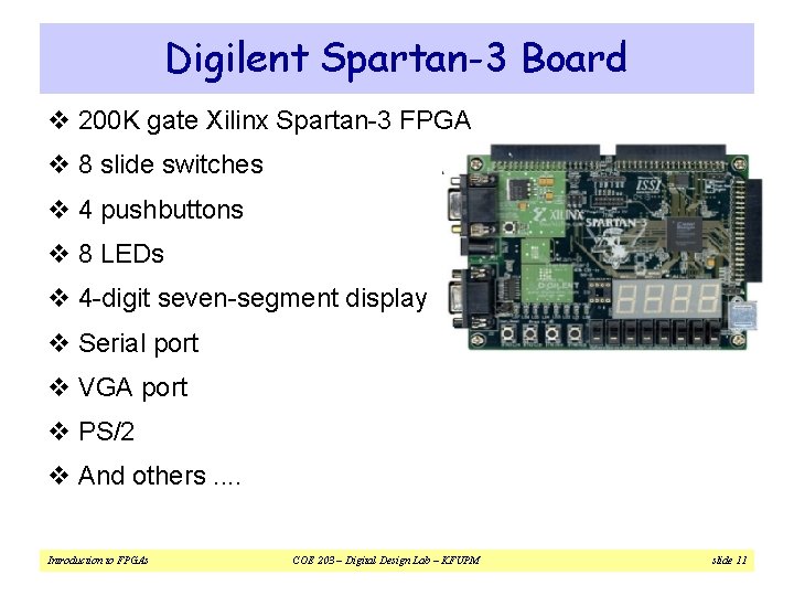
Digilent Spartan-3 Board v 200 K gate Xilinx Spartan-3 FPGA v 8 slide switches v 4 pushbuttons v 8 LEDs v 4 -digit seven-segment display v Serial port v VGA port v PS/2 v And others. . Introduction to FPGAs COE 203 – Digital Design Lab – KFUPM slide 11
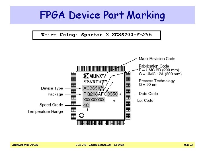
FPGA Device Part Marking We’re Using: Spartan 3 XC 3 S 200 -ft 256 Introduction to FPGAs COE 203 – Digital Design Lab – KFUPM slide 12
- Slides: 12