Introduction to Electronics in HEP Experiments Philippe Farthouat
- Slides: 49

Introduction to Electronics in HEP Experiments Philippe Farthouat CERN Introduction to Electronics Summer 2009 philippe. farthouat@cern. ch

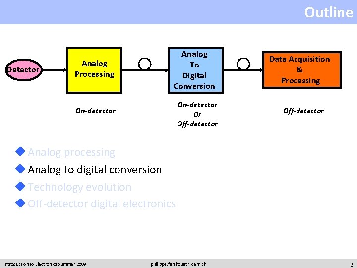
Outline Detector Analog Processing Analog To Digital Conversion On-detector Or Off-detector Data Acquisition & Processing Off-detector u Analog processing u Analog to digital conversion u Technology evolution u Off-detector digital electronics Introduction to Electronics Summer 2009 philippe. farthouat@cern. ch 2

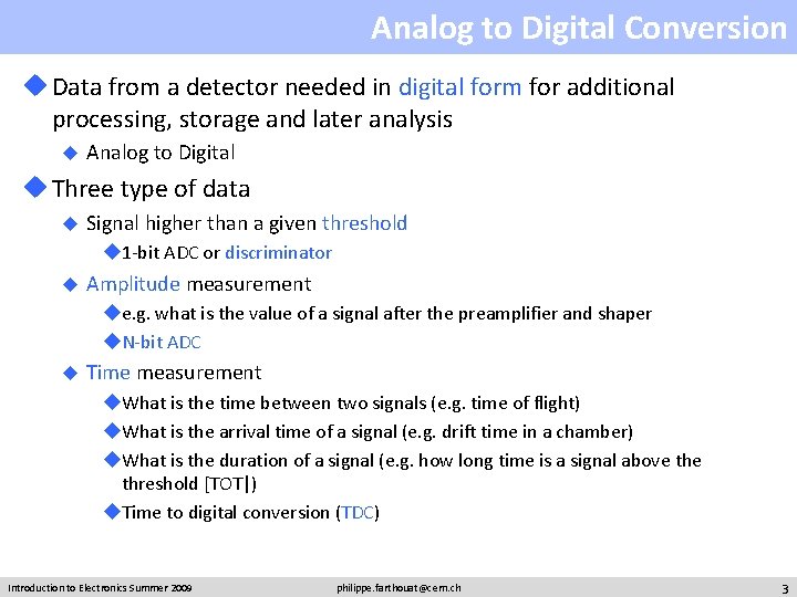
Analog to Digital Conversion u Data from a detector needed in digital form for additional processing, storage and later analysis u Analog to Digital u Three type of data u Signal higher than a given threshold u 1 -bit ADC or discriminator u Amplitude measurement ue. g. what is the value of a signal after the preamplifier and shaper u. N-bit ADC u Time measurement u. What is the time between two signals (e. g. time of flight) u. What is the arrival time of a signal (e. g. drift time in a chamber) u. What is the duration of a signal (e. g. how long time is a signal above threshold [TOT|) u. Time to digital conversion (TDC) Introduction to Electronics Summer 2009 philippe. farthouat@cern. ch 3

Time to Digital Conversion u Introduction u Discriminator u Definition u Time walk u Slewing time u Double-threshold discriminator u Constant fraction discriminator u Different types u Time to Amplitude Converter (TAC) u Wilkinson u “Direct” measurement u Tests Introduction to Electronics Summer 2009 philippe. farthouat@cern. ch 4

What is to be measured? u Time difference between physics signals u Time of flight between two scintillator hodoscopes u Time difference between a physics signal and a logic signal u Time difference between a wire chamber signal and the beam crossing signal u Before feeding a TDC, a physics signal must be transformed in a logic signal in phase with it u Using normalised electrical levels (e. g. NIM, TTL, ECL, LVDS) u This is the role of the discriminator Introduction to Electronics Summer 2009 philippe. farthouat@cern. ch 5

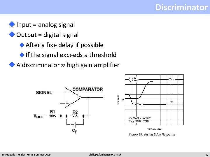
Discriminator u Input = analog signal u Output = digital signal u After a fixe delay if possible u If the signal exceeds a threshold u A discriminator high gain amplifier Introduction to Electronics Summer 2009 philippe. farthouat@cern. ch 6

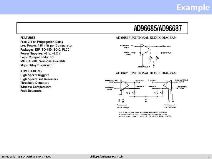
Example Introduction to Electronics Summer 2009 philippe. farthouat@cern. ch 7

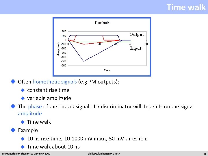
Time walk Output Input u Often homothetic signals (e. g PM outputs): u constant rise time u variable amplitude u The phase of the output signal of a discriminator will depends on the signal amplitude u Time walk u Example u 10 ns rise time, 10 -1000 m. V input, 50 m. V threshold u Time walk about 10 ns Introduction to Electronics Summer 2009 philippe. farthouat@cern. ch 8

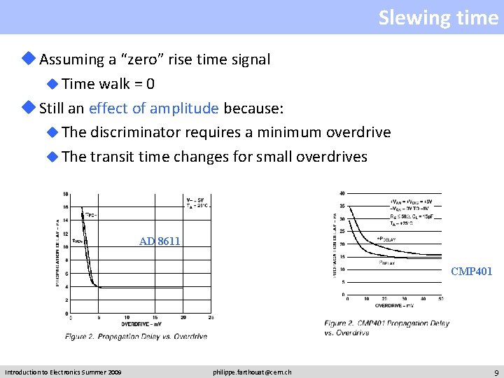
Slewing time u Assuming a “zero” rise time signal u Time walk = 0 u Still an effect of amplitude because: u The discriminator requires a minimum overdrive u The transit time changes for small overdrives AD 8611 CMP 401 Introduction to Electronics Summer 2009 philippe. farthouat@cern. ch 9

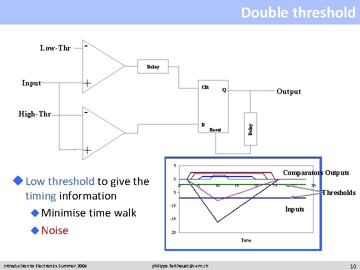
Double threshold Low-Thr Delay High-Thr + Clk Output Q D Reset Delay Input + Comparators Outputs u Low threshold to give the timing information u Minimise time walk u Noise Introduction to Electronics Summer 2009 Thresholds Inputs philippe. farthouat@cern. ch 10

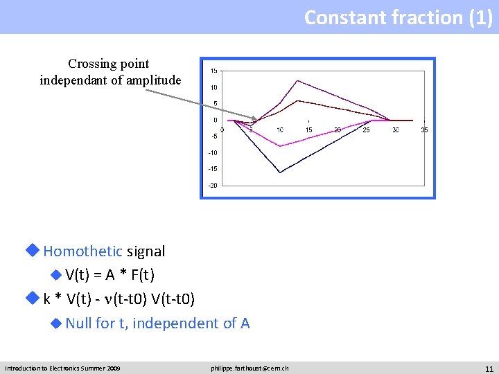
Constant fraction (1) Crossing point independant of amplitude u Homothetic signal u V(t) = A * F(t) u k * V(t) - (t-t 0) V(t-t 0) u Null for t, independent of A Introduction to Electronics Summer 2009 philippe. farthouat@cern. ch 11

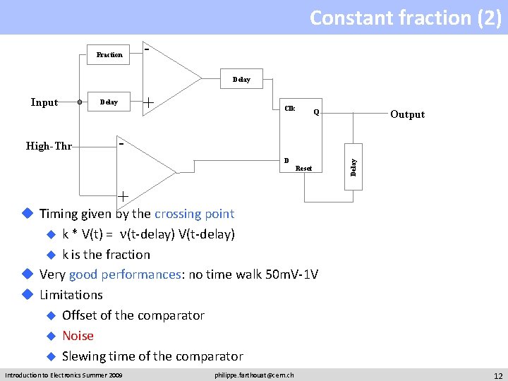
Constant fraction (2) Fraction Delay High-Thr + Delay Clk Output Q D Reset Delay Input + u Timing given by the crossing point u k * V(t) = (t-delay) V(t-delay) u k is the fraction u Very good performances: no time walk 50 m. V-1 V u Limitations u Offset of the comparator u Noise u Slewing time of the comparator Introduction to Electronics Summer 2009 philippe. farthouat@cern. ch 12

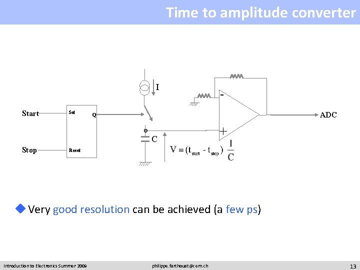
Time to amplitude converter I Start Set ADC Q C Stop - + Reset u Very good resolution can be achieved (a few ps) Introduction to Electronics Summer 2009 philippe. farthouat@cern. ch 13

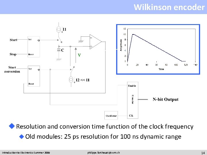
Wilkinson encoder + V u Resolution and conversion time function of the clock frequency u Old modules: 25 ps resolution for 100 ns dynamic range Introduction to Electronics Summer 2009 philippe. farthouat@cern. ch 14

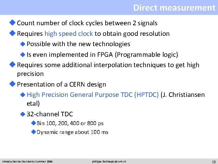
Direct measurement u Count number of clock cycles between 2 signals u Requires high speed clock to obtain good resolution u Possible with the new technologies u Is even implemented in FPGA (Programmable logic) u Requires some additional interpolation techniques to get high precision u Presentation of a CERN design u High Precision General Purpose TDC (HPTDC) (J. Christiansen etal) u 32 -channel TDC u. Bin 100, 200, 400 or 800 ps u. Dynamic range about 100 ms Introduction to Electronics Summer 2009 philippe. farthouat@cern. ch 15

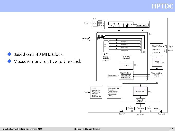
HPTDC u Based on a 40 MHz Clock u Measurement relative to the clock Introduction to Electronics Summer 2009 philippe. farthouat@cern. ch 16

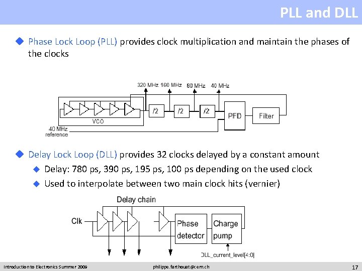
PLL and DLL u Phase Lock Loop (PLL) provides clock multiplication and maintain the phases of the clocks u Delay Lock Loop (DLL) provides 32 clocks delayed by a constant amount u Delay: 780 ps, 390 ps, 195 ps, 100 ps depending on the used clock u Used to interpolate between two main clock hits (vernier) Introduction to Electronics Summer 2009 philippe. farthouat@cern. ch 17

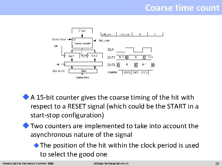
Coarse time count u A 15 -bit counter gives the coarse timing of the hit with respect to a RESET signal (which could be the START in a start-stop configuration) u Two counters are implemented to take into account the asynchronous nature of the signal u The position of the hit within the clock period is used to select the good one Introduction to Electronics Summer 2009 philippe. farthouat@cern. ch 18

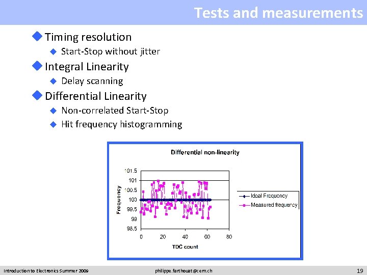
Tests and measurements u Timing resolution u Start-Stop without jitter u Integral Linearity u Delay scanning u Differential Linearity Non-correlated Start-Stop u Hit frequency histogramming u Introduction to Electronics Summer 2009 philippe. farthouat@cern. ch 19

Introduction to Analog to Digital Conversion u Introduction u Conversion errors u Different types of A-to-D converters u Trends in our applications Introduction to Electronics Summer 2009 philippe. farthouat@cern. ch 20

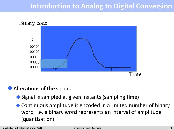
Introduction to Analog to Digital Conversion Binary code …. . 00101 00100 00011 00010 00001 Time u Alterations of the signal: u Signal is sampled at given instants (sampling time) u Continuous amplitude is encoded in a limited number of binary word, i. e. a binary word represents an interval of amplitude (quantization) Introduction to Electronics Summer 2009 philippe. farthouat@cern. ch 21

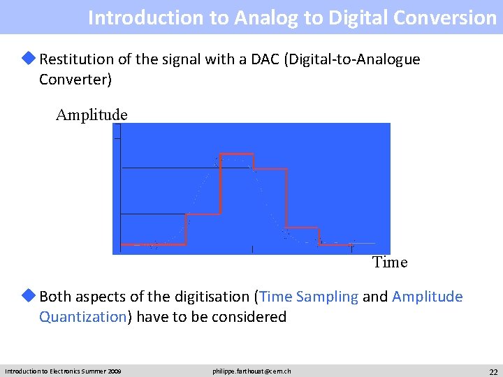
Introduction to Analog to Digital Conversion u Restitution of the signal with a DAC (Digital-to-Analogue Converter) Amplitude Time u Both aspects of the digitisation (Time Sampling and Amplitude Quantization) have to be considered Introduction to Electronics Summer 2009 philippe. farthouat@cern. ch 22

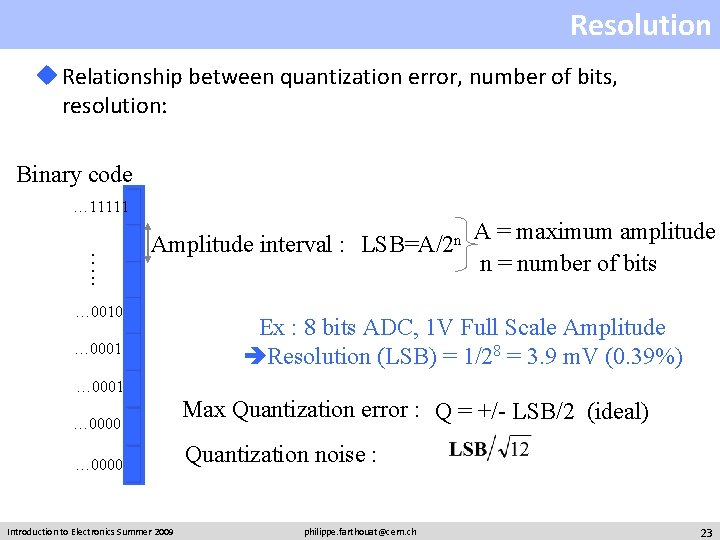
Resolution u Relationship between quantization error, number of bits, resolution: Binary code … 11111 …. . Amplitude interval : … 00100 … 00011 LSB=A/2 n A = maximum amplitude n = number of bits Ex : 8 bits ADC, 1 V Full Scale Amplitude Resolution (LSB) = 1/28 = 3. 9 m. V (0. 39%) … 00010 … 00001 … 00000 Introduction to Electronics Summer 2009 Max Quantization error : Q = +/- LSB/2 (ideal) Quantization noise : philippe. farthouat@cern. ch 23

Dynamic range u Ratio between the minimum and the maximum amplitude to be measured u e. g. calorimeter signal 10 Me. V to 2 Te. V gives a 2 106 dynamic range u In case of a linear system the dynamic range is related to the number of bits (and hence the resolution) u an 8 -bit linear ADC has a 256 dynamic range u In case of large dynamic range, linear systems cannot be used: A calorimeter signal in HEP for which the dynamic range could be as high as 2 106 would require a 21 -bit linear ADC u Some non-linearity is then introduced and there is distinction between dynamic range and resolution. Do not confuse them! u u n-bit resolution u N-bit dynamic range (N>n) u example: u 12 -bit resolution for a 16 -bit dynamic range means that a signal in the range 1 -65000 is measured with a resolution of 0. 02% Introduction to Electronics Summer 2009 philippe. farthouat@cern. ch 24

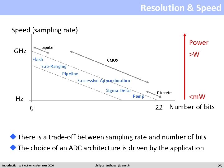
Resolution & Speed (sampling rate) Power bipolar GHz >W Flash CMOS Sub-Ranging Pipeline Successive Approximation Sigma-Delta Hz 6 Ramp Discrete <m. W 22 Number of bits u There is a trade-off between sampling rate and number of bits u The choice of an ADC architecture is driven by the application Introduction to Electronics Summer 2009 philippe. farthouat@cern. ch 25

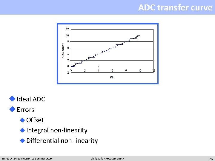
ADC transfer curve u Ideal ADC u Errors u Offset u Integral non-linearity u Differential non-linearity Introduction to Electronics Summer 2009 philippe. farthouat@cern. ch 26

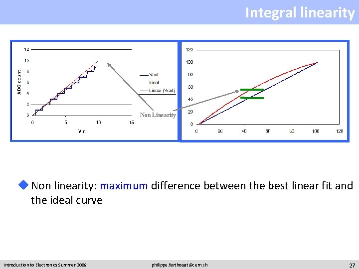
Integral linearity Non Linearity u Non linearity: maximum difference between the best linear fit and the ideal curve Introduction to Electronics Summer 2009 philippe. farthouat@cern. ch 27

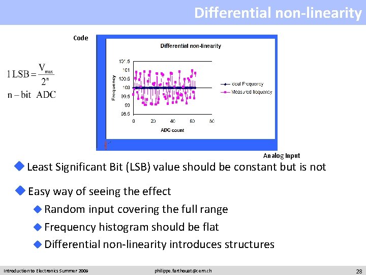
Differential non-linearity Code -0. 6 LSB DNL +0. 5 LSB DNL Analog Input u Least Significant Bit (LSB) value should be constant but is not u Easy way of seeing the effect u Random input covering the full range u Frequency histogram should be flat u Differential non-linearity introduces structures Introduction to Electronics Summer 2009 philippe. farthouat@cern. ch 28

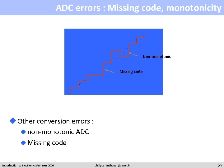
ADC errors : Missing code, monotonicity Non-monotonic Missing code u Other conversion errors : u non-monotonic ADC u Missing code Introduction to Electronics Summer 2009 philippe. farthouat@cern. ch 29

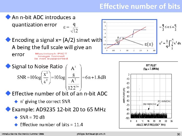
Effective number of bits u An n-bit ADC introduces a quantization error u Encoding a signal x= (A/2) sinwt with A being the full scale will give an error q e(x) u Signal to Noise Ratio u Effective number of bit of an n-bit ADC u n’ giving the correct SNR u Example: AD 9235 12 -bit 20 to 65 MHz SNR = 70 d. B u Effective number of bits = 11. 4 u Introduction to Electronics Summer 2009 philippe. farthouat@cern. ch 30

Types of ADC u Flash ADC & Subranging Flash ADC u Pipeline ADC u Successive Approximation ADC u Ramp ADC u Sigma-Delta Introduction to Electronics Summer 2009 philippe. farthouat@cern. ch 31

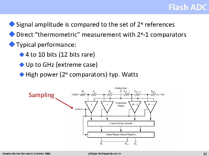
Flash ADC u Signal amplitude is compared to the set of 2 n references u Direct “thermometric” measurement with 2 n-1 comparators u Typical performance: u 4 to 10 bits (12 bits rare) u Up to GHz (extreme case) u High power (2 n comparators) typ. Watts Sampling Introduction to Electronics Summer 2009 philippe. farthouat@cern. ch 32

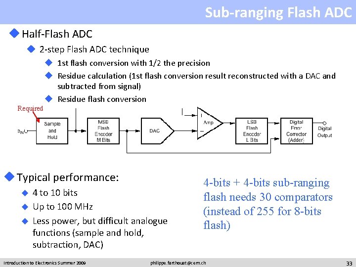
Sub-ranging Flash ADC u Half-Flash ADC u 2 -step Flash ADC technique u 1 st flash conversion with 1/2 the precision u Residue calculation (1 st flash conversion result reconstructed with a DAC and subtracted from signal) u Residue flash conversion Required u Typical performance: 4 to 10 bits u Up to 100 MHz u Less power, but difficult analogue functions (sample and hold, subtraction, DAC) u Introduction to Electronics Summer 2009 4 -bits + 4 -bits sub-ranging flash needs 30 comparators (instead of 255 for 8 -bits flash) philippe. farthouat@cern. ch 33

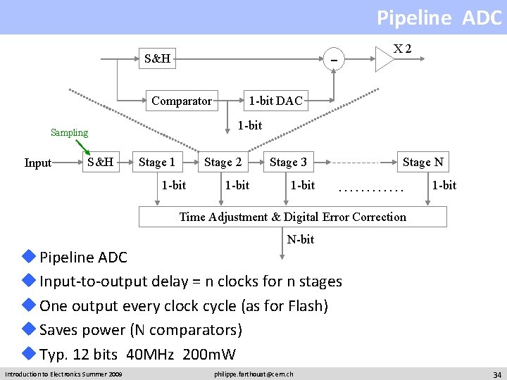
Pipeline ADC - S&H Comparator S&H 1 -bit DAC 1 -bit Sampling Input X 2 Stage 1 Stage 2 1 -bit Stage 3 1 -bit Stage N ………… 1 -bit Time Adjustment & Digital Error Correction N-bit u Pipeline ADC u Input-to-output delay = n clocks for n stages u One output every clock cycle (as for Flash) u Saves power (N comparators) u Typ. 12 bits 40 MHz 200 m. W Introduction to Electronics Summer 2009 philippe. farthouat@cern. ch 34

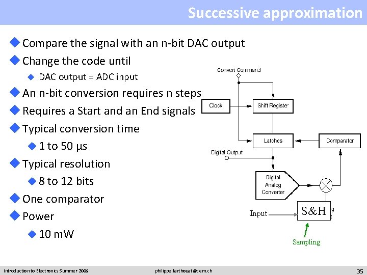
Successive approximation u Compare the signal with an n-bit DAC output u Change the code until u DAC output = ADC input u An n-bit conversion requires n steps u Requires a Start and an End signals u Typical conversion time u 1 to 50 µs u Typical resolution u 8 to 12 bits u One comparator u Power u 10 m. W Introduction to Electronics Summer 2009 philippe. farthouat@cern. ch Input S&H Sampling 35

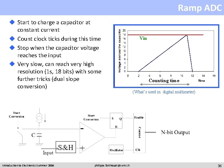
Ramp ADC u Start to charge a capacitor at constant current u Count clock ticks during this time u Stop when the capacitor voltage reaches the input u Very slow, can reach very high resolution (1 s, 18 bits) with some further tricks (dual slope conversion) Input Introduction to Electronics Summer 2009 Vin Counting time (What’s used in digital multimeter) S&H philippe. farthouat@cern. ch 36

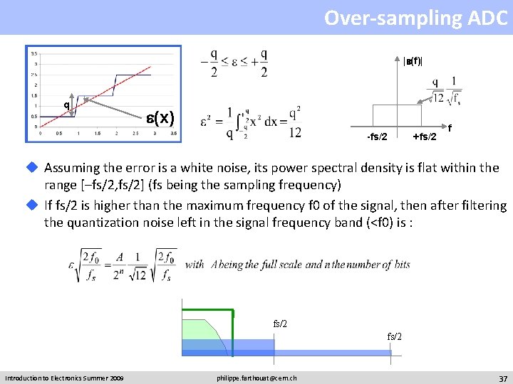
Over-sampling ADC |e(f)| q e(x) -fs/2 +fs/2 f u Assuming the error is a white noise, its power spectral density is flat within the range [–fs/2, fs/2] (fs being the sampling frequency) u If fs/2 is higher than the maximum frequency f 0 of the signal, then after filtering the quantization noise left in the signal frequency band (<f 0) is : fs/2 Introduction to Electronics Summer 2009 philippe. farthouat@cern. ch 37

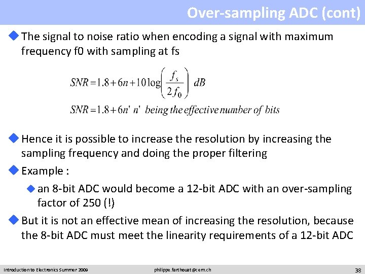
Over-sampling ADC (cont) u The signal to noise ratio when encoding a signal with maximum frequency f 0 with sampling at fs u Hence it is possible to increase the resolution by increasing the sampling frequency and doing the proper filtering u Example : u an 8 -bit ADC would become a 12 -bit ADC with an over-sampling factor of 250 (!) u But it is not an effective mean of increasing the resolution, because the 8 -bit ADC must meet the linearity requirements of a 12 -bit ADC Introduction to Electronics Summer 2009 philippe. farthouat@cern. ch 38

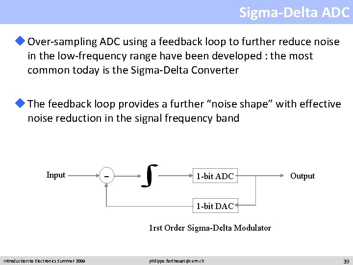
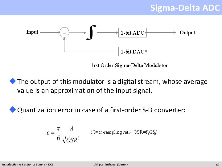
Sigma-Delta ADC u Over-sampling ADC using a feedback loop to further reduce noise in the low-frequency range have been developed : the most common today is the Sigma-Delta Converter u The feedback loop provides a further “noise shape” with effective noise reduction in the signal frequency band Input - 1 -bit ADC Output 1 -bit DAC 1 rst Order Sigma-Delta Modulator Introduction to Electronics Summer 2009 philippe. farthouat@cern. ch 39

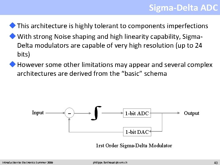
Sigma-Delta ADC u This architecture is highly tolerant to components imperfections u With strong Noise shaping and high linearity capability, Sigma. Delta modulators are capable of very high resolution (up to 24 bits) u However some other limitations may appear and several complex architectures are derived from the “basic” schema Input - 1 -bit ADC Output 1 -bit DAC 1 rst Order Sigma-Delta Modulator Introduction to Electronics Summer 2009 philippe. farthouat@cern. ch 40

Sigma-Delta ADC Input - 1 -bit ADC Output 1 -bit DAC 1 rst Order Sigma-Delta Modulator u The output of this modulator is a digital stream, whose average value is an approximation of the input signal. u Quantization error in case of a first-order S-D converter: (Over-sampling ratio OSR=fs/2 f 0) Introduction to Electronics Summer 2009 philippe. farthouat@cern. ch 41

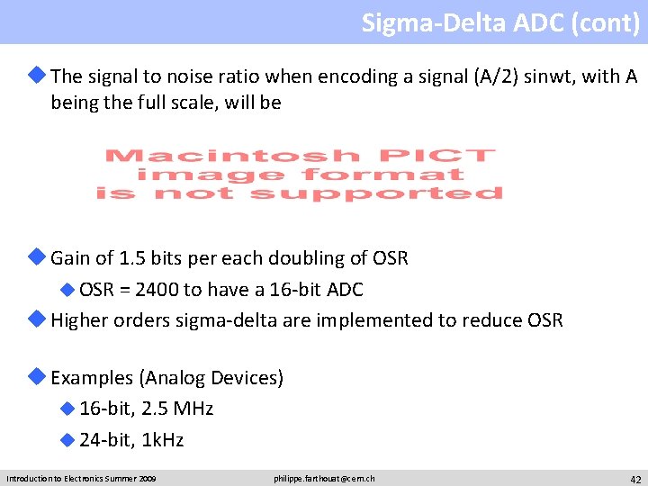
Sigma-Delta ADC (cont) u The signal to noise ratio when encoding a signal (A/2) sinwt, with A being the full scale, will be u Gain of 1. 5 bits per each doubling of OSR u OSR = 2400 to have a 16 -bit ADC u Higher orders sigma-delta are implemented to reduce OSR u Examples (Analog Devices) u 16 -bit, 2. 5 MHz u 24 -bit, 1 k. Hz Introduction to Electronics Summer 2009 philippe. farthouat@cern. ch 42

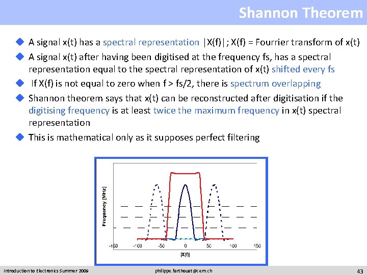
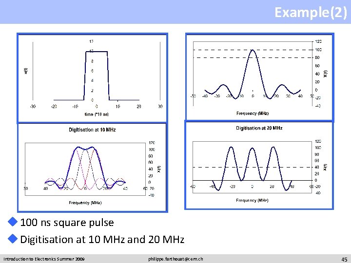
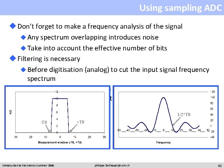
Shannon Theorem u A signal x(t) has a spectral representation |X(f)|; X(f) = Fourrier transform of x(t) u A signal x(t) after having been digitised at the frequency fs, has a spectral representation equal to the spectral representation of x(t) shifted every fs u If X(f) is not equal to zero when f > fs/2, there is spectrum overlapping u Shannon theorem says that x(t) can be reconstructed after digitisation if the digitising frequency is at least twice the maximum frequency in x(t) spectral representation u This is mathematical only as it supposes perfect filtering Introduction to Electronics Summer 2009 philippe. farthouat@cern. ch 43

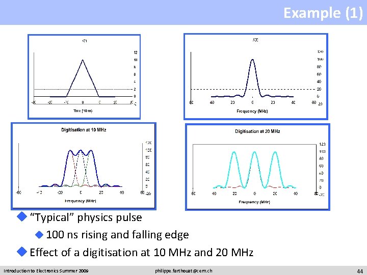
Example (1) u “Typical” physics pulse u 100 ns rising and falling edge u Effect of a digitisation at 10 MHz and 20 MHz Introduction to Electronics Summer 2009 philippe. farthouat@cern. ch 44

Example(2) u 100 ns square pulse u Digitisation at 10 MHz and 20 MHz Introduction to Electronics Summer 2009 philippe. farthouat@cern. ch 45

Using sampling ADC u Don’t forget to make a frequency analysis of the signal u Any spectrum overlapping introduces noise u Take into account the effective number of bits u Filtering is necessary u Before digitisation (analog) to cut the input signal frequency spectrum u After digitisation (digital) to extract the signal frequency spectrum and to compensate the effect of digitisation over a finite time window 1/2*T 0 -T 0 Introduction to Electronics Summer 2009 +T 0 philippe. farthouat@cern. ch 46

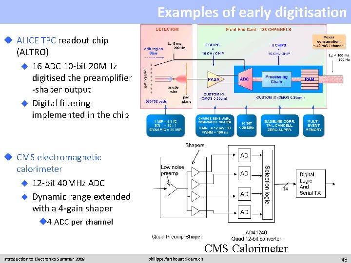
Trends in digitisation u We see more and more the digitisation happening “as soon as possible” in the readout chain u Minimises the difficult problems of handling analog data u. Noise u. Needs for keeping data for a while before a trigger decision arrives ue. g. in LHC experiments, data stored every 25 ns (Bunch crossing period) and trigger decision after sevral µs u Complex filtering for noise optimisation, tails cancelation, … can be done in a digital way in a very efficient and flexible way Introduction to Electronics Summer 2009 philippe. farthouat@cern. ch 47

Examples of early digitisation u ALICE TPC readout chip (ALTRO) u 16 ADC 10 -bit 20 MHz digitised the preamplifier -shaper output u Digital filtering implemented in the chip u CMS electromagnetic calorimeter u 12 -bit 40 MHz ADC u Dynamic range extended with a 4 -gain shaper u 4 ADC per channel CMS Calorimeter Introduction to Electronics Summer 2009 philippe. farthouat@cern. ch 48

Future projects with early digitisation u Super ALTRO for reading out a Linear Collider TPC u 32 or 64 complete channels including the preamplifiers, the 10 bit 10 MHz ADC and the digital data processing u Upgrade of the ATLAS calorimeters for s. LHC u Coding at 40 MHz, 14– 16 -bit u About 200000 channels u For all these applications, very low power ADC are needed u That’s now possible thanks to the evolution of technologies Introduction to Electronics Summer 2009 philippe. farthouat@cern. ch 49