Introduction to Data Conversion EE 174 SJSU Tan
![DNL and INL of ADC k INL (k) = ∑ DNL[i] i=1 DNL and INL of ADC k INL (k) = ∑ DNL[i] i=1](https://slidetodoc.com/presentation_image_h/90ad80910e03491edaa08b6b5e90bec7/image-30.jpg)
![ADC Differential & Integral Nonlinearity Example k INL (k) = ∑ DNL[i] i=1 Notice: ADC Differential & Integral Nonlinearity Example k INL (k) = ∑ DNL[i] i=1 Notice:](https://slidetodoc.com/presentation_image_h/90ad80910e03491edaa08b6b5e90bec7/image-33.jpg)
- Slides: 67

Introduction to Data Conversion EE 174 – SJSU Tan Nguyen

• Introduction to Data Conversion • Introduction to ADC and DAC • DAC specifications • ADC/DAC Performances • Types ADC/DAC

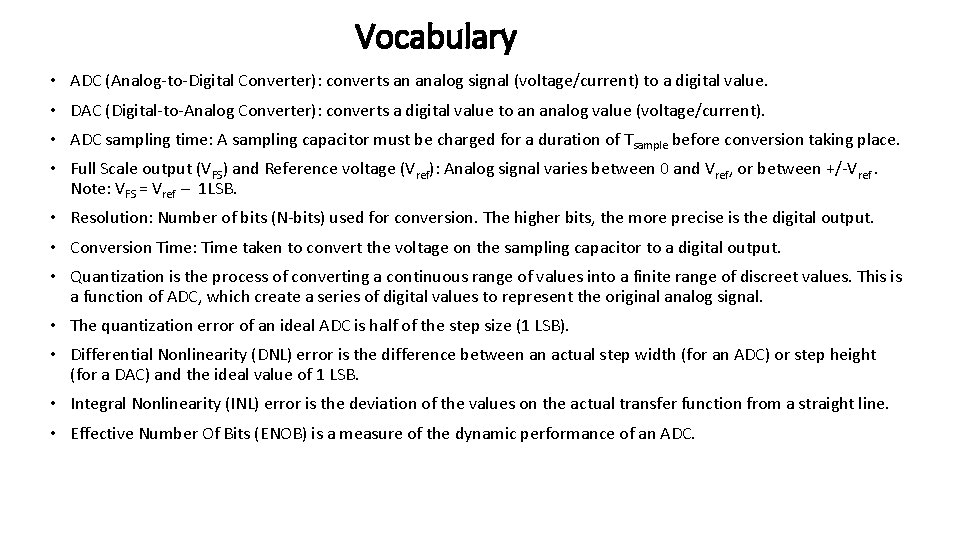
Vocabulary • ADC (Analog-to-Digital Converter): converts an analog signal (voltage/current) to a digital value. • DAC (Digital-to-Analog Converter): converts a digital value to an analog value (voltage/current). • ADC sampling time: A sampling capacitor must be charged for a duration of Tsample before conversion taking place. • Full Scale output (VFS) and Reference voltage (Vref): Analog signal varies between 0 and Vref, or between +/-Vref. Note: VFS = Vref – 1 LSB. • Resolution: Number of bits (N-bits) used for conversion. The higher bits, the more precise is the digital output. • Conversion Time: Time taken to convert the voltage on the sampling capacitor to a digital output. • Quantization is the process of converting a continuous range of values into a finite range of discreet values. This is a function of ADC, which create a series of digital values to represent the original analog signal. • The quantization error of an ideal ADC is half of the step size (1 LSB). • Differential Nonlinearity (DNL) error is the difference between an actual step width (for an ADC) or step height (for a DAC) and the ideal value of 1 LSB. • Integral Nonlinearity (INL) error is the deviation of the values on the actual transfer function from a straight line. • Effective Number Of Bits (ENOB) is a measure of the dynamic performance of an ADC.

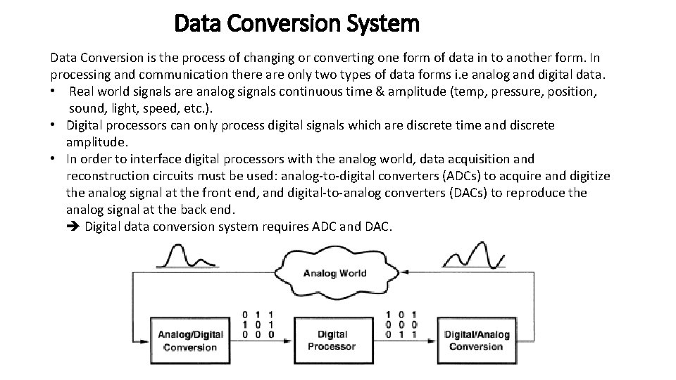
Data Conversion System Data Conversion is the process of changing or converting one form of data in to another form. In processing and communication there are only two types of data forms i. e analog and digital data. • Real world signals are analog signals continuous time & amplitude (temp, pressure, position, sound, light, speed, etc. ). • Digital processors can only process digital signals which are discrete time and discrete amplitude. • In order to interface digital processors with the analog world, data acquisition and reconstruction circuits must be used: analog-to-digital converters (ADCs) to acquire and digitize the analog signal at the front end, and digital-to-analog converters (DACs) to reproduce the analog signal at the back end. Digital data conversion system requires ADC and DAC.

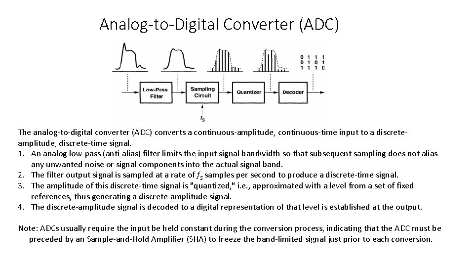
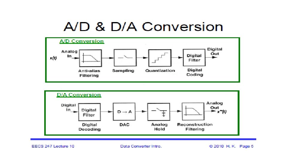
Analog-to-Digital Converter (ADC) The analog-to-digital converter (ADC) converts a continuous-amplitude, continuous-time input to a discreteamplitude, discrete-time signal. 1. An analog low-pass (anti-alias) filter limits the input signal bandwidth so that subsequent sampling does not alias any unwanted noise or signal components into the actual signal band. 2. The filter output signal is sampled at a rate of f. S samples per second to produce a discrete-time signal. 3. The amplitude of this discrete-time signal is "quantized, " i. e. , approximated with a level from a set of fixed references, thus generating a discrete-amplitude signal. 4. The discrete-amplitude signal is decoded to a digital representation of that level is established at the output. Note: ADCs usually require the input be held constant during the conversion process, indicating that the ADC must be preceded by an Sample-and-Hold Amplifier (SHA) to freeze the band-limited signal just prior to each conversion.

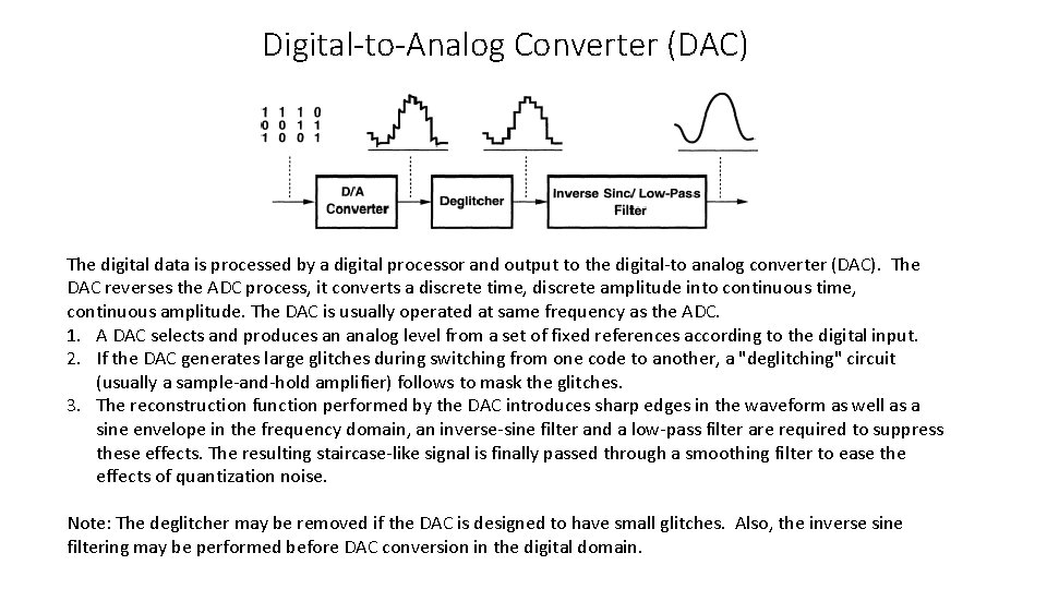
Digital-to-Analog Converter (DAC) The digital data is processed by a digital processor and output to the digital-to analog converter (DAC). The DAC reverses the ADC process, it converts a discrete time, discrete amplitude into continuous time, continuous amplitude. The DAC is usually operated at same frequency as the ADC. 1. A DAC selects and produces an analog level from a set of fixed references according to the digital input. 2. If the DAC generates large glitches during switching from one code to another, a "deglitching" circuit (usually a sample-and-hold amplifier) follows to mask the glitches. 3. The reconstruction function performed by the DAC introduces sharp edges in the waveform as well as a sine envelope in the frequency domain, an inverse-sine filter and a low-pass filter are required to suppress these effects. The resulting staircase-like signal is finally passed through a smoothing filter to ease the effects of quantization noise. Note: The deglitcher may be removed if the DAC is designed to have small glitches. Also, the inverse sine filtering may be performed before DAC conversion in the digital domain.

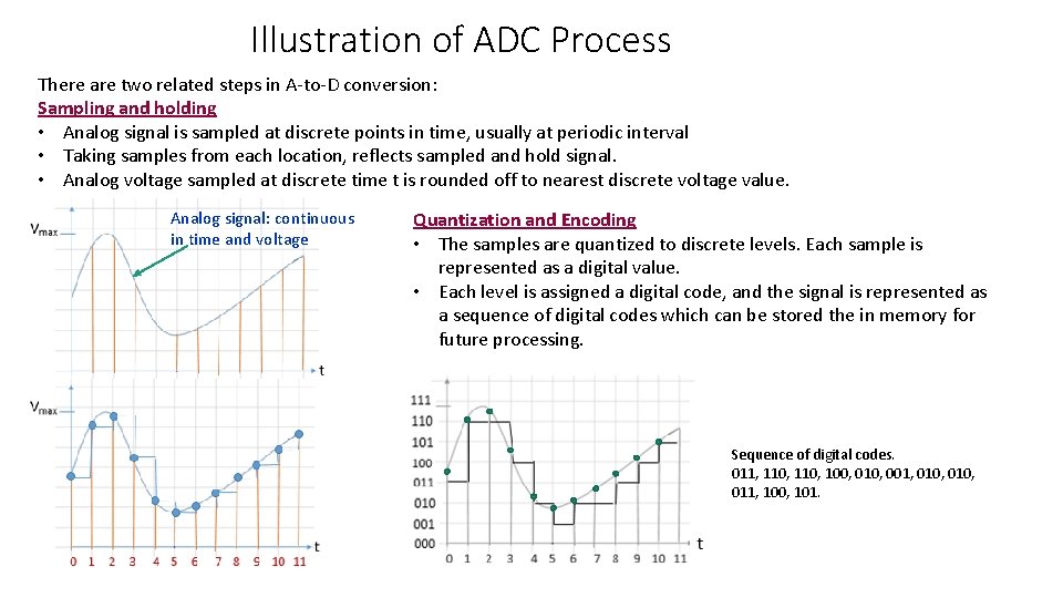
Illustration of ADC Process There are two related steps in A-to-D conversion: Sampling and holding • Analog signal is sampled at discrete points in time, usually at periodic interval • Taking samples from each location, reflects sampled and hold signal. • Analog voltage sampled at discrete time t is rounded off to nearest discrete voltage value. Analog signal: continuous in time and voltage Quantization and Encoding • The samples are quantized to discrete levels. Each sample is represented as a digital value. • Each level is assigned a digital code, and the signal is represented as a sequence of digital codes which can be stored the in memory for future processing. Sequence of digital codes. 011, 110, 100, 010, 001, 010, 011, 100, 101.

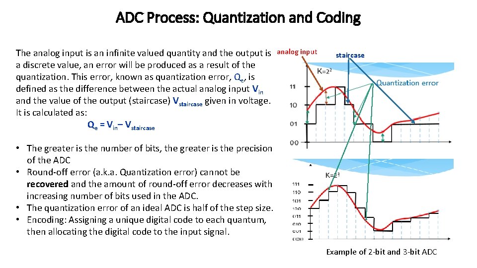
ADC Process: Quantization and Coding The analog input is an infinite valued quantity and the output is a discrete value, an error will be produced as a result of the quantization. This error, known as quantization error, Qe, is defined as the difference between the actual analog input Vin and the value of the output (staircase) Vstaircase given in voltage. It is calculated as: Qe = Vin– Vstaircase analog input staircase • The greater is the number of bits, the greater is the precision of the ADC • Round-off error (a. k. a. Quantization error) cannot be recovered and the amount of round-off error decreases with increasing number of bits used in the ADC. • The quantization error of an ideal ADC is half of the step size. • Encoding: Assigning a unique digital code to each quantum, then allocating the digital code to the input signal. Example of 2 -bit and 3 -bit ADC

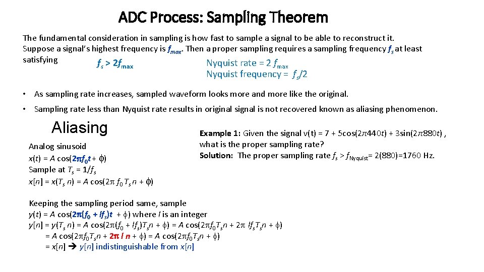
ADC Process: Sampling Theorem The fundamental consideration in sampling is how fast to sample a signal to be able to reconstruct it. Suppose a signal’s highest frequency is fmax. Then a proper sampling requires a sampling frequency fs at least satisfying f > 2 f Nyquist rate = 2 f s max Nyquist frequency = fs/2 • As sampling rate increases, sampled waveform looks more and more like the original. • Sampling rate less than Nyquist rate results in original signal is not recovered known as aliasing phenomenon. Aliasing Analog sinusoid x(t) = A cos(2 pf 0 t + f) Sample at Ts = 1/fs x[n] = x(Ts n) = A cos(2 p f 0 Ts n + f) Example 1: Given the signal v(t) = 7 + 5 cos(2π440 t) + 3 sin(2π880 t) , what is the proper sampling rate? Solution: The proper sampling rate fs > f. Nyquist= 2(880)=1760 Hz. Keeping the sampling period same, sample y(t) = A cos(2 p(f 0 + lfs)t + f) where l is an integer y[n] = y(Ts n) = A cos(2 p(f 0 + lfs)Tsn + f) = A cos(2 pf 0 Tsn + 2 p lfs. Tsn + f) = A cos(2 pf 0 Tsn + 2 p l n + f) = A cos(2 pf 0 Tsn + f) = x[n] y[n] indistinguishable from x[n]

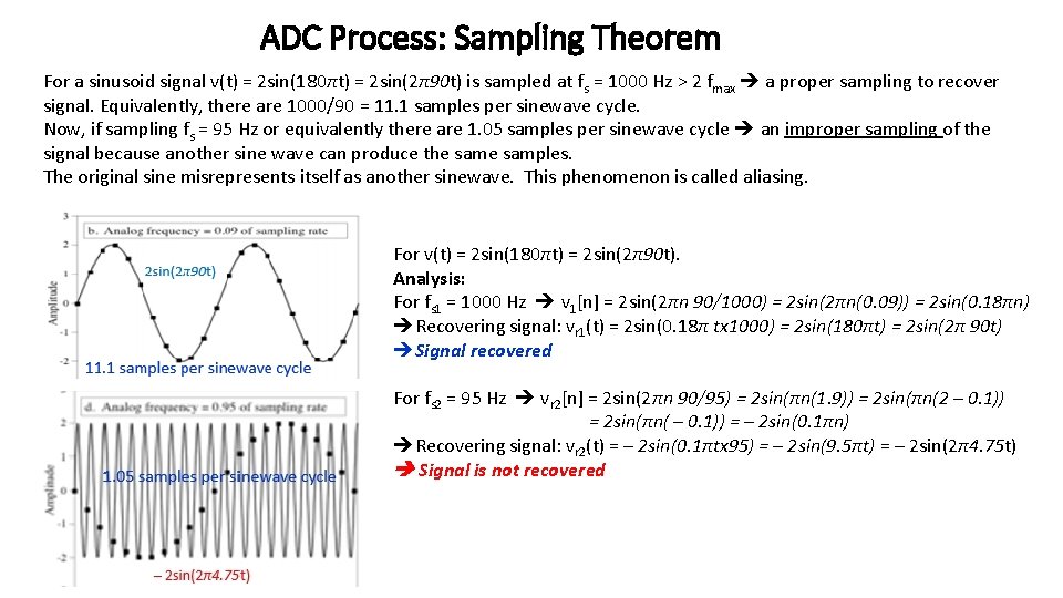
ADC Process: Sampling Theorem For a sinusoid signal v(t) = 2 sin(180πt) = 2 sin(2π90 t) is sampled at fs = 1000 Hz > 2 fmax a proper sampling to recover signal. Equivalently, there are 1000/90 = 11. 1 samples per sinewave cycle. Now, if sampling fs = 95 Hz or equivalently there are 1. 05 samples per sinewave cycle an improper sampling of the signal because another sine wave can produce the samples. The original sine misrepresents itself as another sinewave. This phenomenon is called aliasing. For v(t) = 2 sin(180πt) = 2 sin(2π90 t). Analysis: For fs 1 = 1000 Hz v 1[n] = 2 sin(2πn 90/1000) = 2 sin(2πn(0. 09)) = 2 sin(0. 18πn) Recovering signal: vr 1(t) = 2 sin(0. 18π tx 1000) = 2 sin(180πt) = 2 sin(2π 90 t) Signal recovered For fs 2 = 95 Hz vr 2[n] = 2 sin(2πn 90/95) = 2 sin(πn(1. 9)) = 2 sin(πn(2 – 0. 1)) = 2 sin(πn( – 0. 1)) = – 2 sin(0. 1πn) Recovering signal: vr 2(t) = – 2 sin(0. 1πtx 95) = – 2 sin(9. 5πt) = – 2 sin(2π4. 75 t) Signal is not recovered

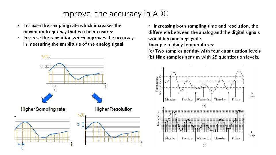
Improve the accuracy in ADC • Increase the sampling rate which increases the maximum frequency that can be measured. • Increase the resolution which improves the accuracy in measuring the amplitude of the analog signal. • Increasing both sampling time and resolution, the difference between the analog and the digital signals would become negligible Example of daily temperatures: (a) Two samples per day with four quantization levels (b) Nine samples per day with 25 quantization levels.

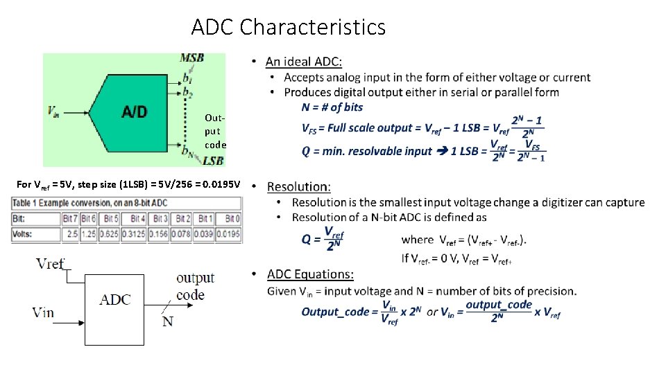
ADC Characteristics Output code For Vref = 5 V, step size (1 LSB) = 5 V/256 = 0. 0195 V

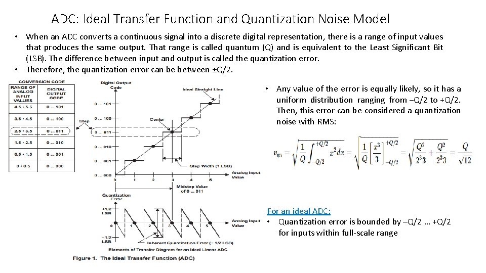
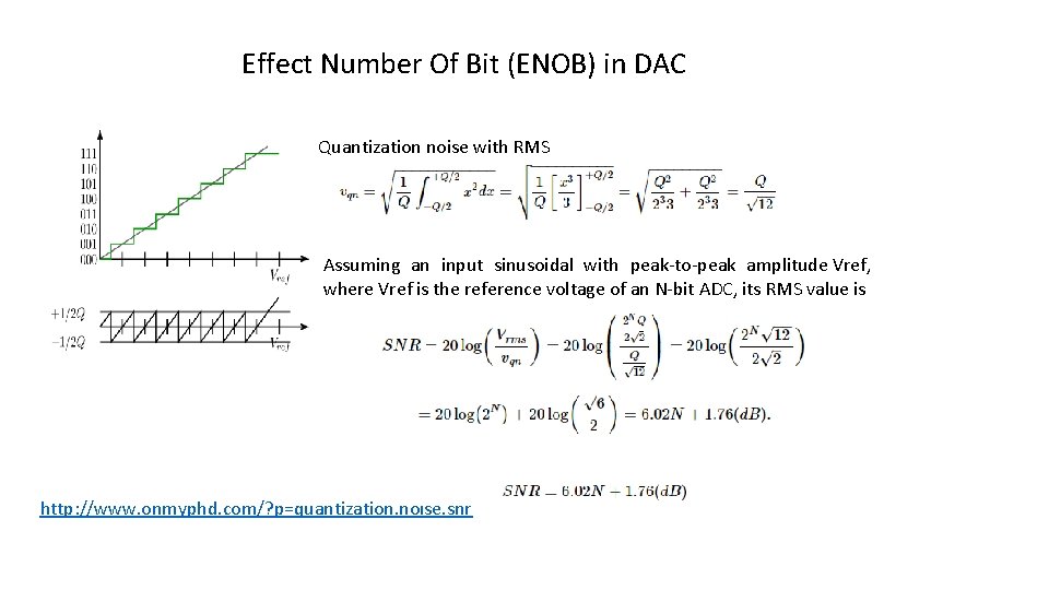
ADC: Ideal Transfer Function and Quantization Noise Model • When an ADC converts a continuous signal into a discrete digital representation, there is a range of input values that produces the same output. That range is called quantum (Q) and is equivalent to the Least Significant Bit (LSB). The difference between input and output is called the quantization error. • Therefore, the quantization error can be between ±Q/2. • Any value of the error is equally likely, so it has a uniform distribution ranging from −Q/2 to +Q/2. Then, this error can be considered a quantization noise with RMS: For an ideal ADC: • Quantization error is bounded by –Q/2 … +Q/2 for inputs within full-scale range

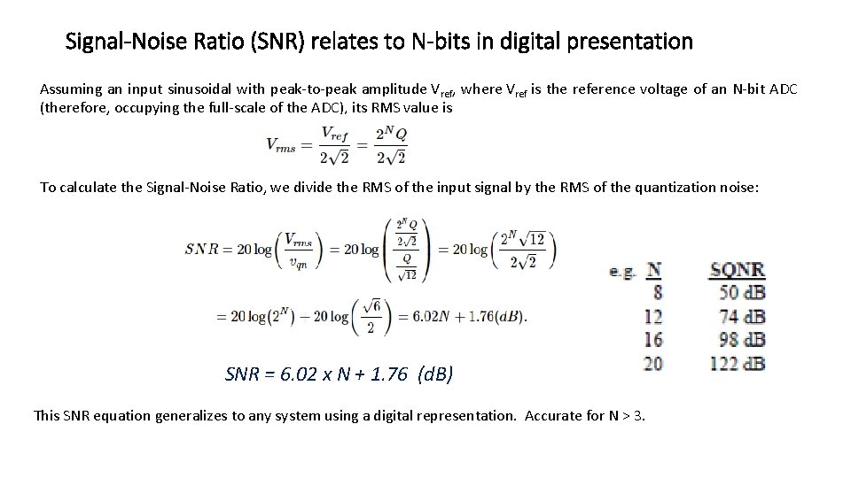
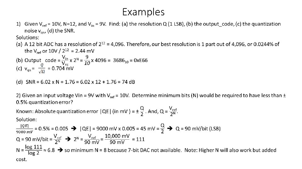
Signal-Noise Ratio (SNR) relates to N-bits in digital presentation Assuming an input sinusoidal with peak-to-peak amplitude Vref, where Vref is the reference voltage of an N-bit ADC (therefore, occupying the full-scale of the ADC), its RMS value is To calculate the Signal-Noise Ratio, we divide the RMS of the input signal by the RMS of the quantization noise: SNR = 6. 02 x N + 1. 76 (d. B) This SNR equation generalizes to any system using a digital representation. Accurate for N > 3.

Examples

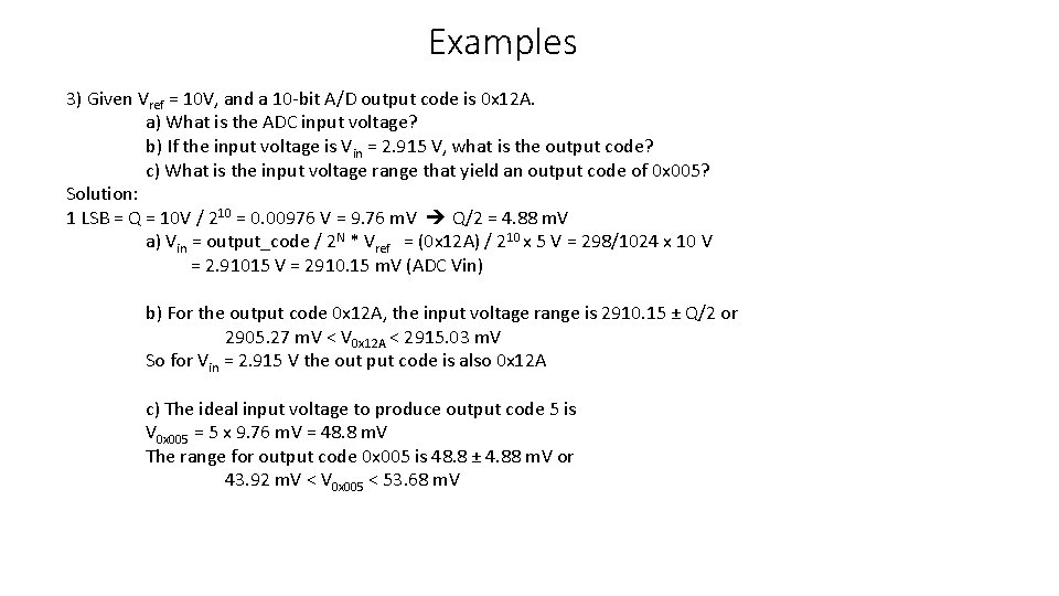
Examples 3) Given Vref = 10 V, and a 10 -bit A/D output code is 0 x 12 A. a) What is the ADC input voltage? b) If the input voltage is Vin = 2. 915 V, what is the output code? c) What is the input voltage range that yield an output code of 0 x 005? Solution: 1 LSB = Q = 10 V / 210 = 0. 00976 V = 9. 76 m. V Q/2 = 4. 88 m. V a) Vin = output_code / 2 N * Vref = (0 x 12 A) / 210 x 5 V = 298/1024 x 10 V = 2. 91015 V = 2910. 15 m. V (ADC Vin) b) For the output code 0 x 12 A, the input voltage range is 2910. 15 ± Q/2 or 2905. 27 m. V < V 0 x 12 A < 2915. 03 m. V So for Vin = 2. 915 V the out put code is also 0 x 12 A c) The ideal input voltage to produce output code 5 is V 0 x 005 = 5 x 9. 76 m. V = 48. 8 m. V The range for output code 0 x 005 is 48. 8 ± 4. 88 m. V or 43. 92 m. V < V 0 x 005 < 53. 68 m. V

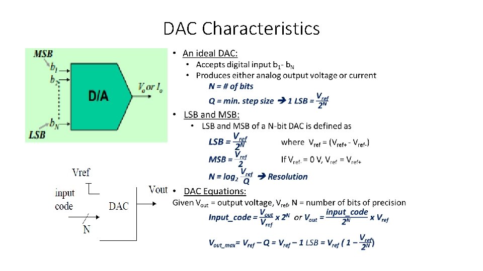
DAC Characteristics

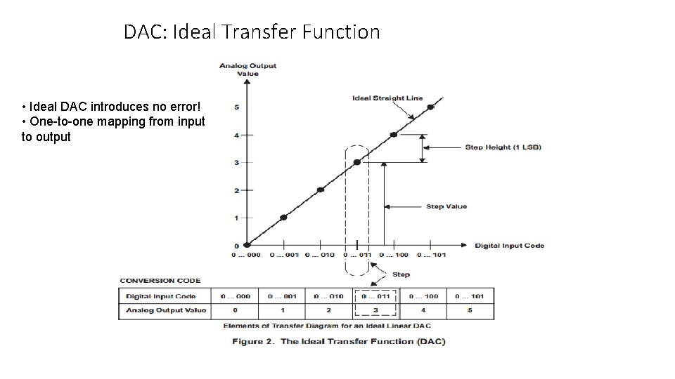
DAC: Ideal Transfer Function DAC • Ideal DAC introduces no error! • One-to-one mapping from input to output

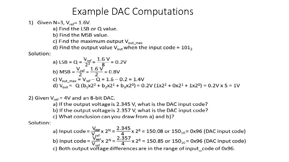
Example DAC Computations

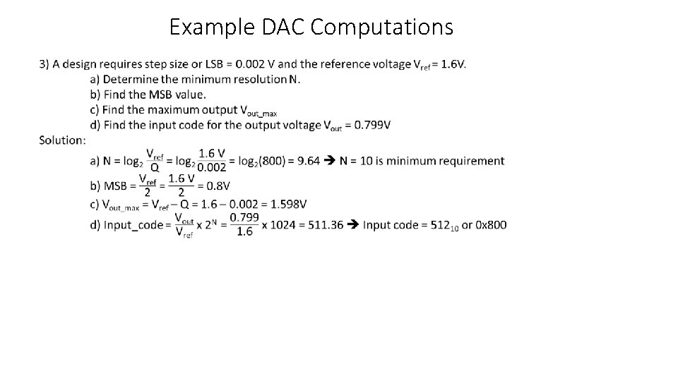
Example DAC Computations

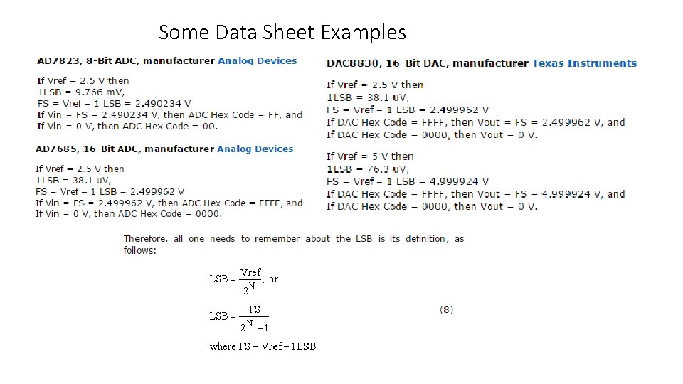
Some Data Sheet Examples

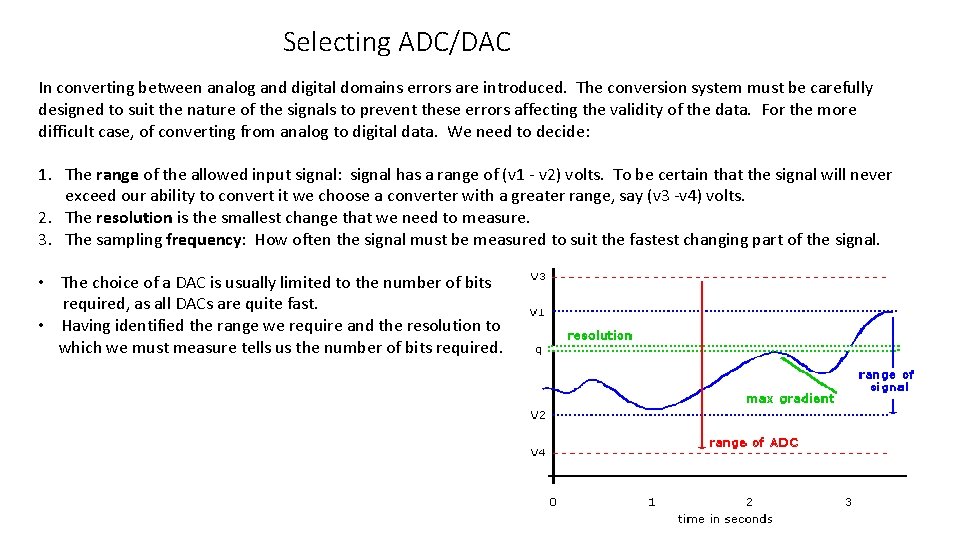
Selecting ADC/DAC In converting between analog and digital domains errors are introduced. The conversion system must be carefully designed to suit the nature of the signals to prevent these errors affecting the validity of the data. For the more difficult case, of converting from analog to digital data. We need to decide: 1. The range of the allowed input signal: signal has a range of (v 1 - v 2) volts. To be certain that the signal will never exceed our ability to convert it we choose a converter with a greater range, say (v 3 -v 4) volts. 2. The resolution is the smallest change that we need to measure. 3. The sampling frequency: How often the signal must be measured to suit the fastest changing part of the signal. • The choice of a DAC is usually limited to the number of bits required, as all DACs are quite fast. • Having identified the range we require and the resolution to which we must measure tells us the number of bits required.

Data Converter Performance Metric EE 174 – SJSU Tan Nguyen

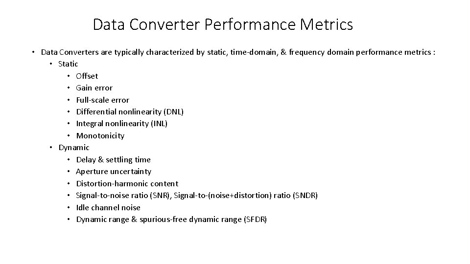
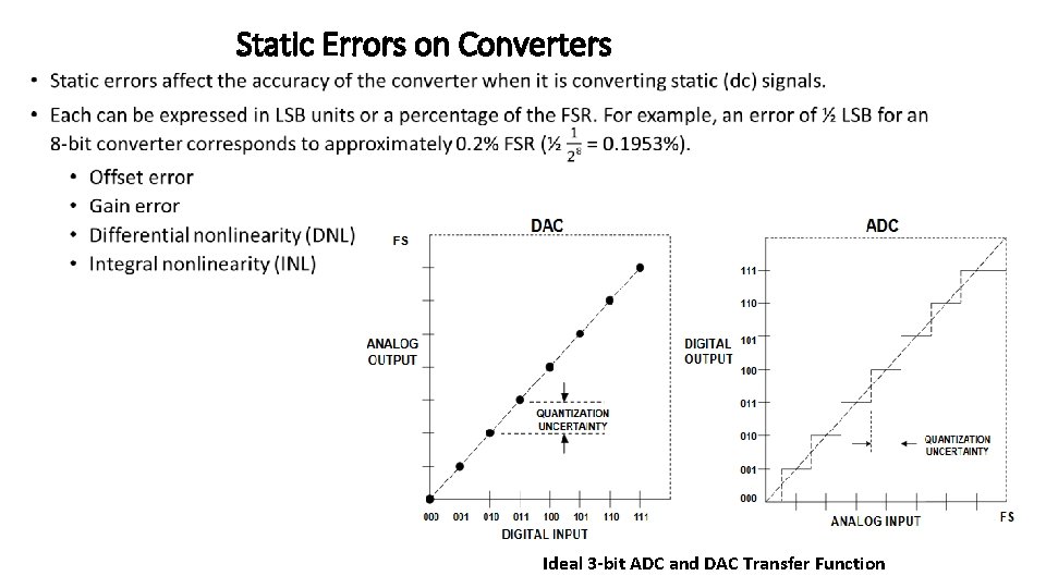
Data Converter Performance Metrics • Data Converters are typically characterized by static, time-domain, & frequency domain performance metrics : • Static • Offset • Gain error • Full-scale error • Differential nonlinearity (DNL) • Integral nonlinearity (INL) • Monotonicity • Dynamic • Delay & settling time • Aperture uncertainty • Distortion-harmonic content • Signal-to-noise ratio (SNR), Signal-to-(noise+distortion) ratio (SNDR) • Idle channel noise • Dynamic range & spurious-free dynamic range (SFDR)

Static Errors on Converters • Ideal 3 -bit ADC and DAC Transfer Function

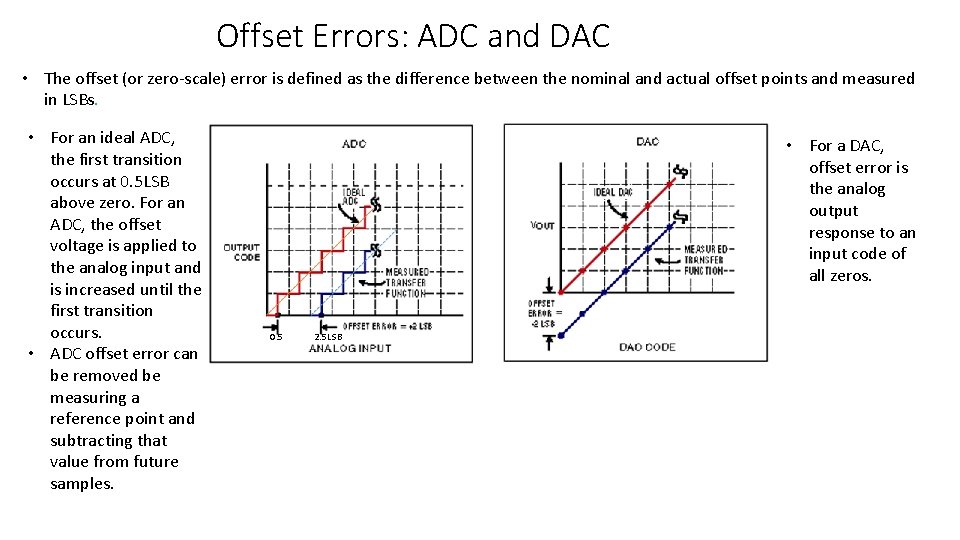
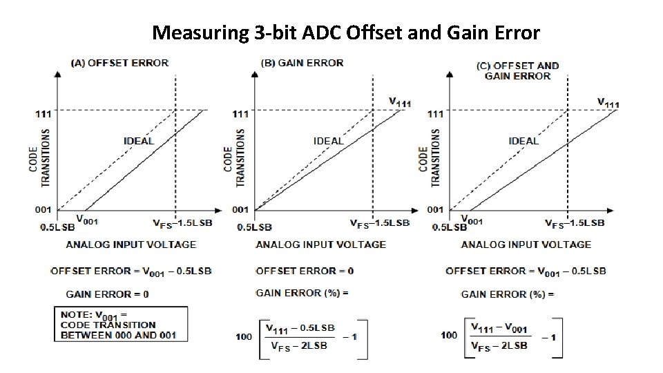
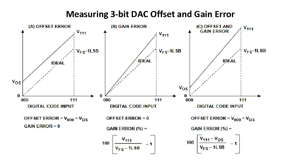
Error (Zaoand scale. DAC er) Offset Errors: ADC • The offset (or zero-scale) error is defined as the difference between the nominal and actual offset points and measured in LSBs. • For an ideal ADC, the first transition occurs at 0. 5 LSB above zero. For an ADC, the offset voltage is applied to the analog input and is increased until the first transition occurs. • ADC offset error can be removed be measuring a reference point and subtracting that value from future samples. • For a DAC, offset error is the analog output response to an input code of all zeros. 0. 5 2. 5 LSB

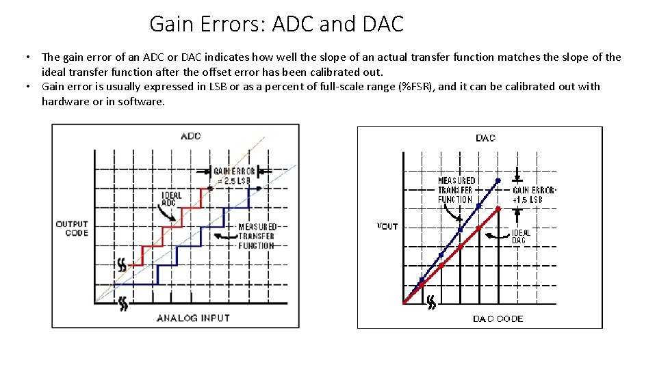
Gain Errors: ADC and DAC Gain Error • The gain error of an ADC or DAC indicates how well the slope of an actual transfer function matches the slope of the ideal transfer function after the offset error has been calibrated out. • Gain error is usually expressed in LSB or as a percent of full-scale range (%FSR), and it can be calibrated out with hardware or in software.

Measuring 3 -bit ADC Offset and Gain Error

Measuring 3 -bit DAC Offset and Gain Error
![DNL and INL of ADC k INL k DNLi i1 DNL and INL of ADC k INL (k) = ∑ DNL[i] i=1](https://slidetodoc.com/presentation_image_h/90ad80910e03491edaa08b6b5e90bec7/image-30.jpg)
DNL and INL of ADC k INL (k) = ∑ DNL[i] i=1

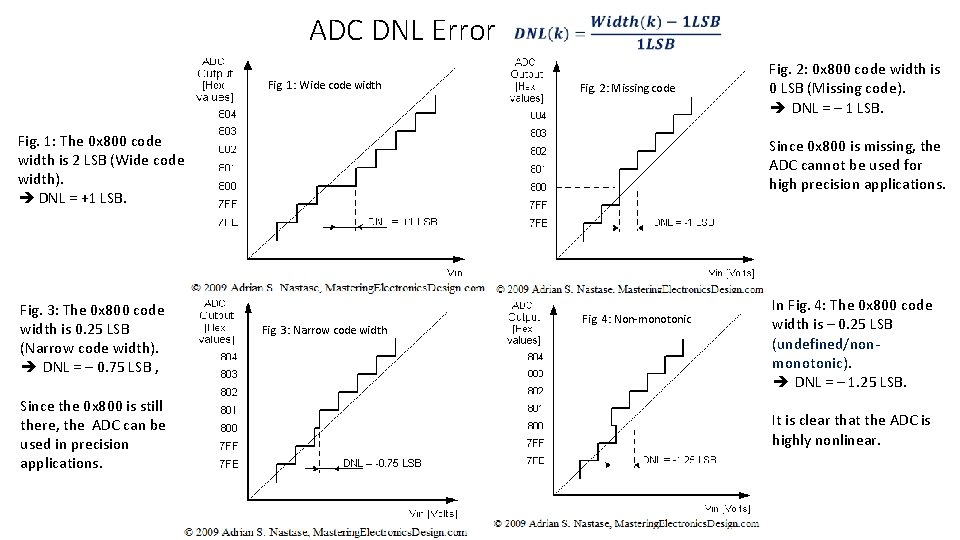
ADC DNL Error Fig. 1: Wide code width Fig. 2: Missing code Fig. 1: The 0 x 800 code width is 2 LSB (Wide code width). DNL = +1 LSB. Fig. 3: The 0 x 800 code width is 0. 25 LSB (Narrow code width). DNL = – 0. 75 LSB , Since the 0 x 800 is still there, the ADC can be used in precision applications. Fig. 2: 0 x 800 code width is 0 LSB (Missing code). DNL = – 1 LSB. Since 0 x 800 is missing, the ADC cannot be used for high precision applications. Fig. 3: Narrow code width Fig. 4: Non-monotonic In Fig. 4: The 0 x 800 code width is – 0. 25 LSB (undefined/non- monotonic). DNL = – 1. 25 LSB. It is clear that the ADC is highly nonlinear.

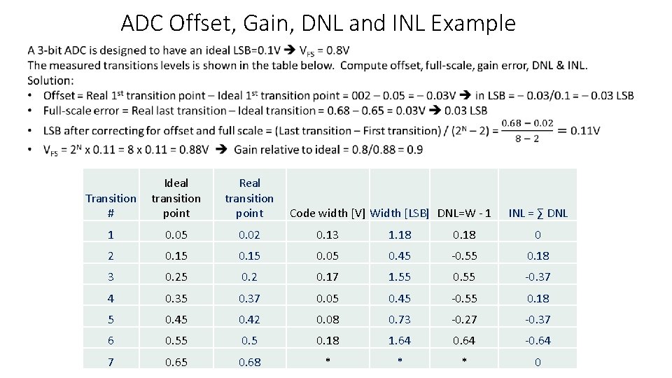
ADC Offset, Gain, DNL and INL Example Ideal Transition transition # point Real transition point Code width [V] Width [LSB] DNL=W - 1 INL = ∑ DNL 1 0. 05 0. 02 0. 13 1. 18 0 2 0. 15 0. 05 0. 45 -0. 55 0. 18 3 0. 25 0. 2 0. 17 1. 55 0. 55 -0. 37 4 0. 35 0. 37 0. 05 0. 45 -0. 55 0. 18 5 0. 42 0. 08 0. 73 -0. 27 -0. 37 6 0. 55 0. 18 1. 64 0. 64 -0. 64 7 0. 65 0. 68 * * * 0
![ADC Differential Integral Nonlinearity Example k INL k DNLi i1 Notice ADC Differential & Integral Nonlinearity Example k INL (k) = ∑ DNL[i] i=1 Notice:](https://slidetodoc.com/presentation_image_h/90ad80910e03491edaa08b6b5e90bec7/image-33.jpg)
ADC Differential & Integral Nonlinearity Example k INL (k) = ∑ DNL[i] i=1 Notice: For end-point corrected measurement INL[0] undefined INL[1]=0 INL[2 N-1]=0

Effect Number Of Bit (ENOB) in DAC Quantization noise with RMS Assuming an input sinusoidal with peak-to-peak amplitude Vref, where Vref is the reference voltage of an N-bit ADC, its RMS value is http: //www. onmyphd. com/? p=quantization. noise. snr

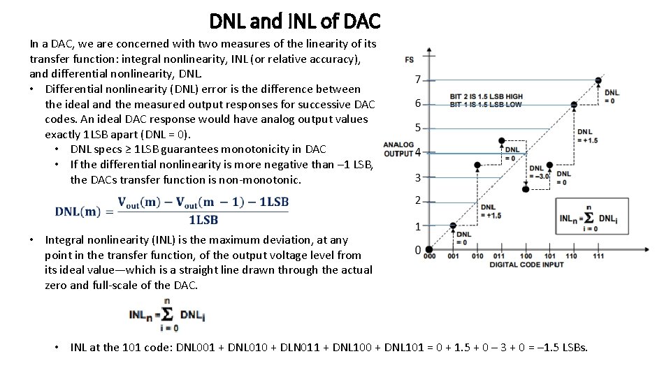
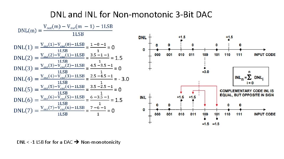
DNL and INL of DAC In a DAC, we are concerned with two measures of the linearity of its transfer function: integral nonlinearity, INL (or relative accuracy), and differential nonlinearity, DNL. • Differential nonlinearity (DNL) error is the difference between the ideal and the measured output responses for successive DAC codes. An ideal DAC response would have analog output values exactly 1 LSB apart (DNL = 0). • DNL specs ≥ 1 LSB guarantees monotonicity in DAC • If the differential nonlinearity is more negative than – 1 LSB, the DACs transfer function is non-monotonic. • Integral nonlinearity (INL) is the maximum deviation, at any point in the transfer function, of the output voltage level from its ideal value—which is a straight line drawn through the actual zero and full-scale of the DAC. • INL at the 101 code: DNL 001 + DNL 010 + DLN 011 + DNL 100 + DNL 101 = 0 + 1. 5 + 0 – 3 + 0 = – 1. 5 LSBs.

DNL and INL for Non-monotonic 3 -Bit DAC DNL < -1 LSB for a DAC Non-monotonicity

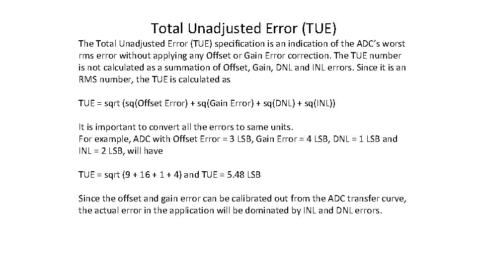
Total Unadjusted Error (TUE) The Total Unadjusted Error (TUE) specification is an indication of the ADC’s worst rms error without applying any Offset or Gain Error correction. The TUE number is not calculated as a summation of Offset, Gain, DNL and INL errors. Since it is an RMS number, the TUE is calculated as TUE = sqrt (sq(Offset Error) + sq(Gain Error) + sq(DNL) + sq(INL)) It is important to convert all the errors to same units. For example, ADC with Offset Error = 3 LSB, Gain Error = 4 LSB, DNL = 1 LSB and INL = 2 LSB, will have TUE = sqrt (9 + 16 + 1 + 4) and TUE = 5. 48 LSB Since the offset and gain error can be calibrated out from the ADC transfer curve, the actual error in the application will be dominated by INL and DNL errors.

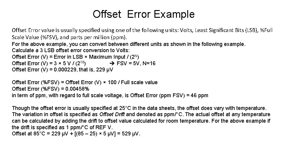
Offset Error Example Offset Error value is usually specified using one of the following units: Volts, Least Significant Bits (LSB), %Full Scale Value (%FSV), and parts per million (ppm). For the above example, you can convert between different units as shown in the following example. Calculate a 3 LSB offset error conversion to Volts: Offset Error (V) = Error in LSB × Maximum Input / (2 N) Offset Error (V) = 3 × 5 V / (216) FSV = 5 V, N=16 Offset Error (V) = 0. 000229, that is, 229 μV spacer Offset Error (%FSV) = Offset Error (V) × 100 / Full scale value Offset Error (%FSV) = 0. 00458% in term of ppm, with regard to full scale voltage, is Offset Error (ppm FSV) = 46 ppm Though the offset error is usually specified at 25°C in the data sheets, the offset does vary with temperature. The variation in offset is specified as Offset Drift and denoted as ppm/°C. The actual offset at any temperature can be calculated by adding the drift to offset value calculated for room temperature. For the above example if the drift is specified as 1 ppm/°C of REF V. Offset at 85°C = 229 μV + [(85 – 25) × 5 μV] = 529 μV.

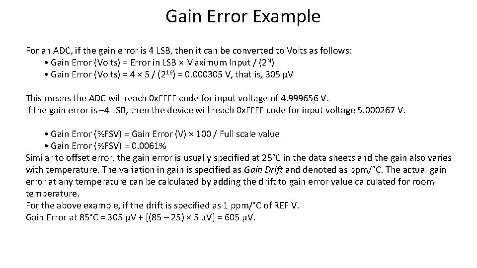
Gain Error Example For an ADC, if the gain error is 4 LSB, then it can be converted to Volts as follows: • Gain Error (Volts) = Error in LSB × Maximum Input / (2 N) • Gain Error (Volts) = 4 × 5 / (216) = 0. 000305 V, that is, 305 μV This means the ADC will reach 0 x. FFFF code for input voltage of 4. 999656 V. If the gain error is – 4 LSB, then the device will reach 0 x. FFFF code for input voltage 5. 000267 V. • Gain Error (%FSV) = Gain Error (V) × 100 / Full scale value • Gain Error (%FSV) = 0. 0061% Similar to offset error, the gain error is usually specified at 25°C in the data sheets and the gain also varies with temperature. The variation in gain is specified as Gain Drift and denoted as ppm/°C. The actual gain error at any temperature can be calculated by adding the drift to gain error value calculated for room temperature. For the above example, if the drift is specified as 1 ppm/°C of REF V. Gain Error at 85°C = 305 μV + [(85 – 25) × 5 μV] = 605 μV.

Types of ADC • • Flash ADC Successive approximation converter Counter Ramp Converter Integrating ADC

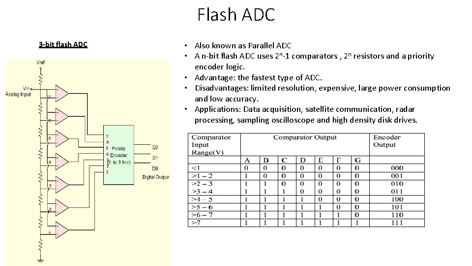
Flash ADC 3 -bit flash ADC • Also known as Parallel ADC • A n-bit flash ADC uses 2 n-1 comparators , 2 n resistors and a priority encoder logic. • Advantage: the fastest type of ADC. • Disadvantages: limited resolution, expensive, large power consumption and low accuracy. • Applications: Data acquisition, satellite communication, radar processing, sampling oscilloscope and high density disk drives. 7 6 5 4 3 2 1

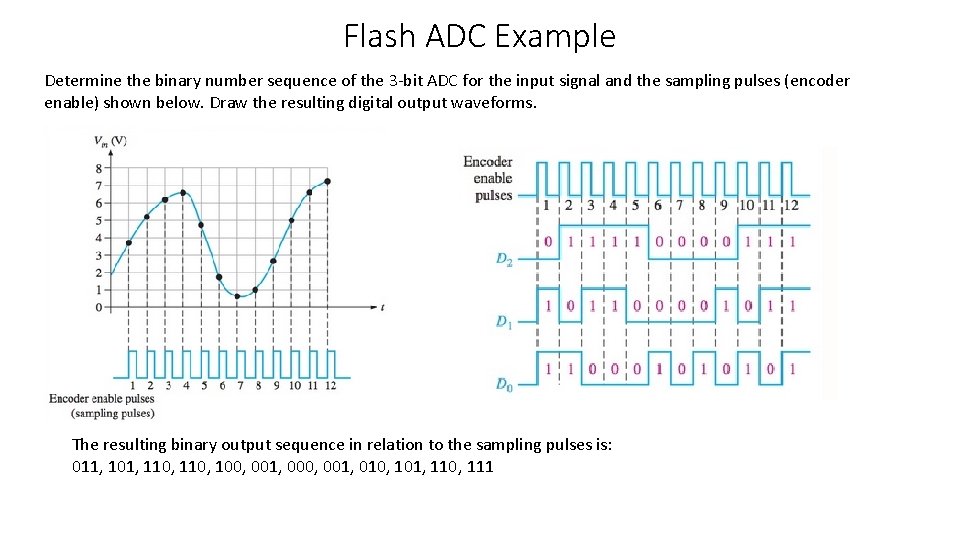
Flash ADC Example Determine the binary number sequence of the 3 -bit ADC for the input signal and the sampling pulses (encoder enable) shown below. Draw the resulting digital output waveforms. The resulting binary output sequence in relation to the sampling pulses is: 011, 101, 110, 100, 001, 010, 101, 110, 111

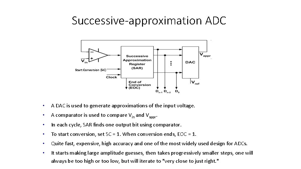
Successive-approximation ADC Start Conversion (SC) • A DAC is used to generate approximations of the input voltage. • A comparator is used to compare Vin and Vappr. • In each cycle, SAR finds one output bit using comparator. • To start conversion, set SC = 1. When conversion ends, EOC = 1. • Quite fast, expensive, high accuracy and one of the most widely used design for ADCs. • It starts making large amplitude guesses, then takes progressively smaller steps, one will always be too high or too low, but will iterate to "very close to just right. "

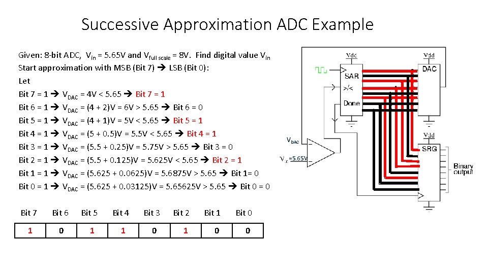
Successive Approximation ADC Example Given: 8 -bit ADC, Vin = 5. 65 V and Vfull scale = 8 V. Find digital value Vin Start approximation with MSB (Bit 7) LSB (Bit 0): Let Bit 7 = 1 VDAC = 4 V < 5. 65 Bit 7 = 1 Bit 6 = 1 VDAC = (4 + 2)V = 6 V > 5. 65 Bit 6 = 0 Bit 5 = 1 VDAC = (4 + 1)V = 5 V < 5. 65 Bit 5 = 1 Bit 4 = 1 VDAC = (5 + 0. 5)V = 5. 5 V < 5. 65 Bit 4 = 1 Bit 3 = 1 VDAC = (5. 5 + 0. 25)V = 5. 75 V > 5. 65 Bit 3 = 0 Bit 2 = 1 VDAC = (5. 5 + 0. 125)V = 5. 625 V < 5. 65 Bit 2 = 1 Bit 1 = 1 VDAC = (5. 625 + 0. 0625)V = 5. 6875 V > 5. 65 Bit 1= 0 Bit 0 = 1 VDAC = (5. 625 + 0. 03125)V = 5. 65625 V > 5. 65 Bit 0 = 0 Bit 7 Bit 6 Bit 5 Bit 4 Bit 3 Bit 2 Bit 1 Bit 0 1 0 1 0 0 VDAC = 5. 65 V

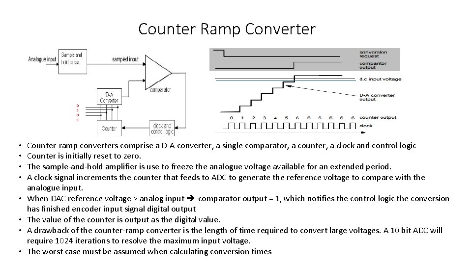
Counter Ramp Converter 0 1 • • Counter-ramp converters comprise a D-A converter, a single comparator, a counter, a clock and control logic Counter is initially reset to zero. The sample-and-hold amplifier is use to freeze the analogue voltage available for an extended period. A clock signal increments the counter that feeds to ADC to generate the reference voltage to compare with the analogue input. When DAC reference voltage > analog input comparator output = 1, which notifies the control logic the conversion has finished encoder input signal digital output The value of the counter is output as the digital value. A drawback of the counter-ramp converter is the length of time required to convert large voltages. A 10 bit ADC will require 1024 iterations to resolve the maximum input voltage. The worst case must be assumed when calculating conversion times

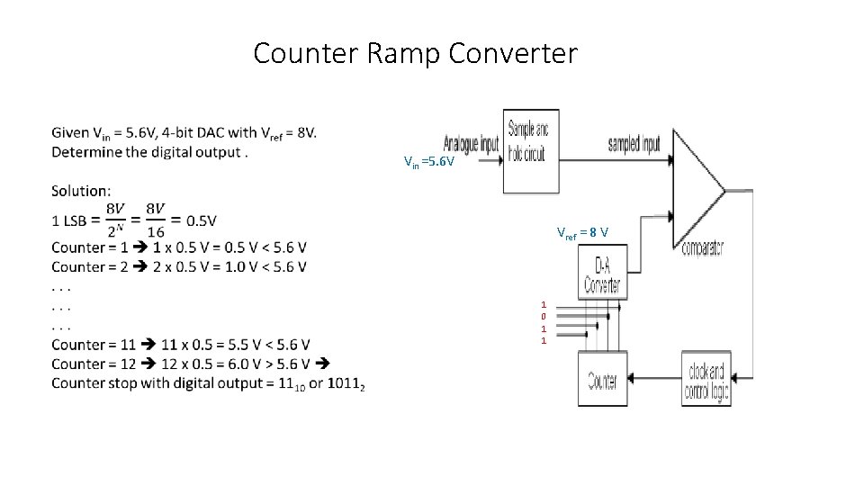
Counter Ramp Converter Vin =5. 6 V Vref = 8 V 1 0 1 1

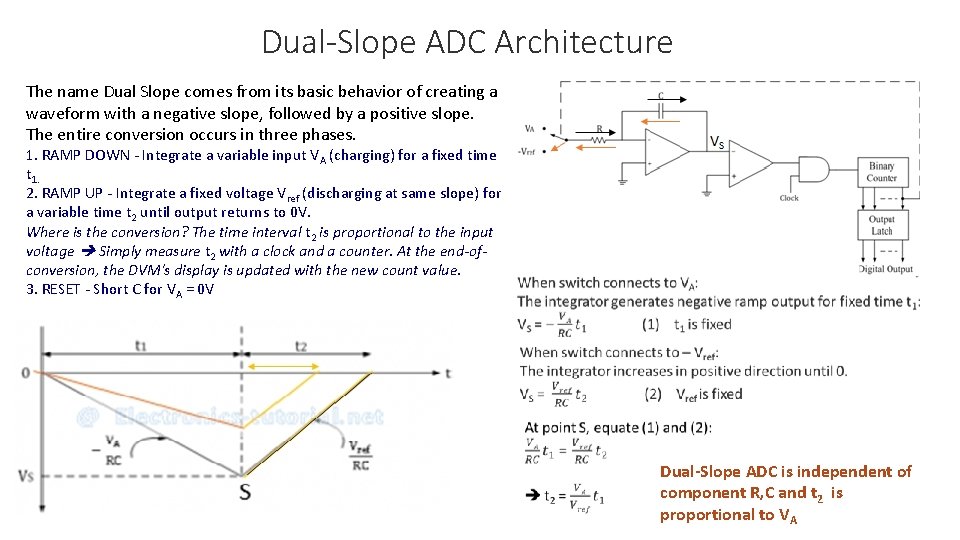
Dual-Slope ADC Architecture The name Dual Slope comes from its basic behavior of creating a waveform with a negative slope, followed by a positive slope. The entire conversion occurs in three phases. 1. RAMP DOWN - Integrate a variable input VA (charging) for a fixed time t 1. 2. RAMP UP - Integrate a fixed voltage Vref (discharging at same slope) for a variable time t 2 until output returns to 0 V. Where is the conversion? The time interval t 2 is proportional to the input voltage Simply measure t 2 with a clock and a counter. At the end-ofconversion, the DVM's display is updated with the new count value. 3. RESET - Short C for VA = 0 V Dual-Slope ADC is independent of component R, C and t 2 is proportional to VA

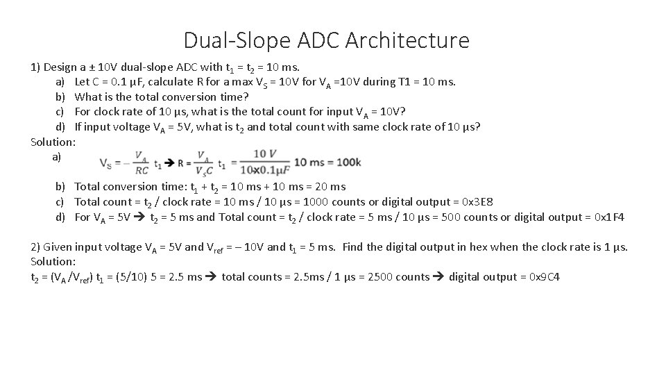
Dual-Slope ADC Architecture 1) Design a ± 10 V dual-slope ADC with t 1 = t 2 = 10 ms. a) Let C = 0. 1 µF, calculate R for a max VS = 10 V for VA =10 V during T 1 = 10 ms. b) What is the total conversion time? c) For clock rate of 10 µs, what is the total count for input VA = 10 V? d) If input voltage VA = 5 V, what is t 2 and total count with same clock rate of 10 µs? Solution: a) b) Total conversion time: t 1 + t 2 = 10 ms + 10 ms = 20 ms c) Total count = t 2 / clock rate = 10 ms / 10 µs = 1000 counts or digital output = 0 x 3 E 8 d) For VA = 5 V t 2 = 5 ms and Total count = t 2 / clock rate = 5 ms / 10 µs = 500 counts or digital output = 0 x 1 F 4 2) Given input voltage VA = 5 V and Vref = – 10 V and t 1 = 5 ms. Find the digital output in hex when the clock rate is 1 µs. Solution: t 2 = (VA /Vref) t 1 = (5/10) 5 = 2. 5 ms total counts = 2. 5 ms / 1 µs = 2500 counts digital output = 0 x 9 C 4

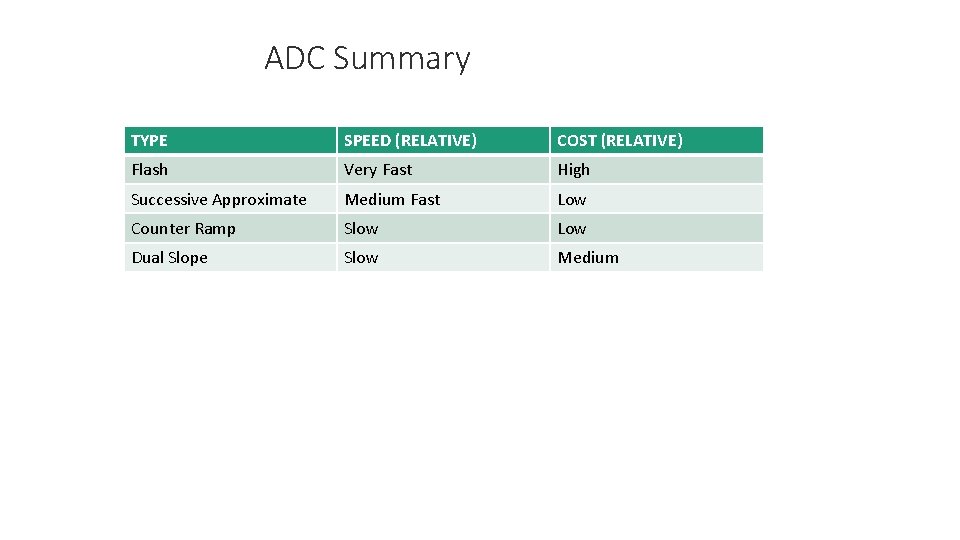
ADC Summary TYPE SPEED (RELATIVE) COST (RELATIVE) Flash Very Fast High Successive Approximate Medium Fast Low Counter Ramp Slow Low Dual Slope Slow Medium

Types of DAC • Binary Weighted Resistor • R-2 R (Non-inverting and Inverting) Ladder

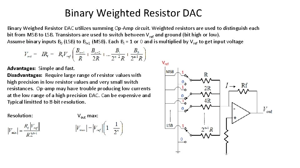
Binary Weighted Resistor DAC Binary Weighed Resistor DAC utilizes summing Op-Amp circuit. Weighted resistors are used to distinguish each bit from MSB to LSB. Transistors are used to switch between Vref and ground (bit high or low). Assume binary inputs B 0 (LSB) to Bn-1 (MSB). Each Bi = 1 or 0 and is multiplied by Vref to get input voltage Advantages: Simple and fast. Disadvantages: Require large range of resistor values with high precision in low resistor values and very small switch resistances. Op-amp may have trouble producing low currents at the low range of a high precision DAC. Can be expensive and Typical limitted to 8 -bit resolution. Resolution: Vout max:

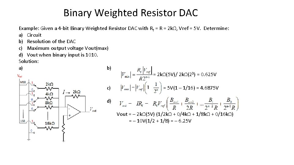
Binary Weighted Resistor DAC Example: Given a 4 -bit Binary Weighted Resistor DAC with Rf = R = 2 kΩ, Vref = 5 V. Determine: a) Circuit b) Resolution of the DAC c) Maximum output voltage Vout(max) d) Vout when binary input is 1010. Solution: a) b) = 2 kΩ(5 V)/ 2 kΩ(23) = 0. 625 V c) = 5 V(1 – 1/16) = 4. 6875 V d) Vout = – 2 kΩ(5 V) (1/2 kΩ + 0/4 kΩ + 1/8 kΩ + 0/16 kΩ) = – 10 V(1/2 + 1/8) = – 6. 25 V

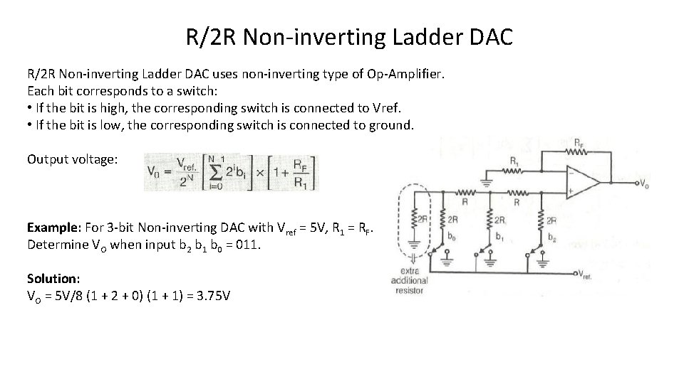
R/2 R Non-inverting Ladder DAC uses non-inverting type of Op-Amplifier. Each bit corresponds to a switch: • If the bit is high, the corresponding switch is connected to Vref. • If the bit is low, the corresponding switch is connected to ground. Output voltage: Example: For 3 -bit Non-inverting DAC with Vref = 5 V, R 1 = RF. Determine VO when input b 2 b 1 b 0 = 011. Solution: VO = 5 V/8 (1 + 2 + 0) (1 + 1) = 3. 75 V

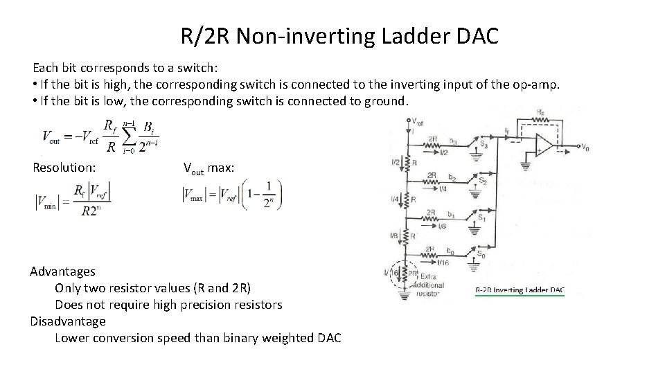
R/2 R Non-inverting Ladder DAC Each bit corresponds to a switch: • If the bit is high, the corresponding switch is connected to the inverting input of the op-amp. • If the bit is low, the corresponding switch is connected to ground. Resolution: Vout max: Advantages Only two resistor values (R and 2 R) Does not require high precision resistors Disadvantage Lower conversion speed than binary weighted DAC

Sampling and Reconstruction of Signal

x(t) x~(t)

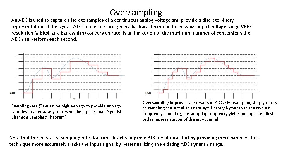
Oversampling An ADC is used to capture discrete samples of a continuous analog voltage and provide a discrete binary representation of the signal. ADC converters are generally characterized in three ways: input voltage range VREF, resolution (# bits), and bandwidth (conversion rate) is an indication of the maximum number of conversions the ADC can perform each second. Sampling rate (T) must be high enough to provide enough samples to adequately represent the input signal (Nyquist. Shannon Sampling Theorem). Oversampling improves the results of ADC. Oversampling simply refers to sampling the signal at a rate significantly higher than the Nyquist Frequency. Doubling the sampling frequency yields an improved firstorder representation of the input signal Note that the increased sampling rate does not directly improve ADC resolution, but by providing more samples, this technique more accurately tracks the input signal by better utilizing the existing ADC dynamic range.

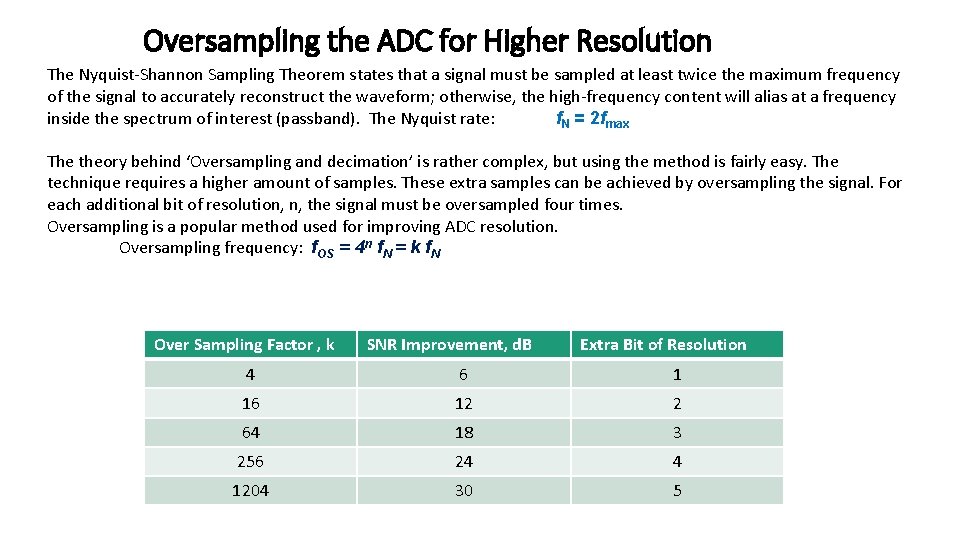
Oversampling the ADC for Higher Resolution The Nyquist-Shannon Sampling Theorem states that a signal must be sampled at least twice the maximum frequency of the signal to accurately reconstruct the waveform; otherwise, the high-frequency content will alias at a frequency inside the spectrum of interest (passband). The Nyquist rate: f. N = 2 fmax The theory behind ‘Oversampling and decimation’ is rather complex, but using the method is fairly easy. The technique requires a higher amount of samples. These extra samples can be achieved by oversampling the signal. For each additional bit of resolution, n, the signal must be oversampled four times. Oversampling is a popular method used for improving ADC resolution. Oversampling frequency: f. OS = 4 n f. N = k f. N Over Sampling Factor , k SNR Improvement, d. B Extra Bit of Resolution 4 6 1 16 12 2 64 18 3 256 24 4 1204 30 5

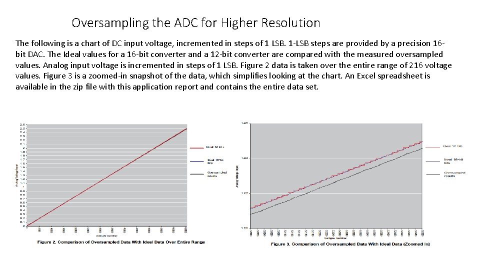
Oversampling the ADC for Higher Resolution The following is a chart of DC input voltage, incremented in steps of 1 LSB. 1 -LSB steps are provided by a precision 16 bit DAC. The Ideal values for a 16 -bit converter and a 12 -bit converter are compared with the measured oversampled values. Analog input voltage is incremented in steps of 1 LSB. Figure 2 data is taken over the entire range of 216 voltage values. Figure 3 is a zoomed-in snapshot of the data, which simplifies looking at the chart. An Excel spreadsheet is available in the zip file with this application report and contains the entire data set.

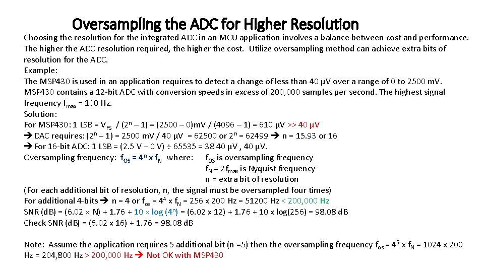
Oversampling the ADC for Higher Resolution Choosing the resolution for the integrated ADC in an MCU application involves a balance between cost and performance. The higher the ADC resolution required, the higher the cost. Utilize oversampling method can achieve extra bits of resolution for the ADC. Example: The MSP 430 is used in an application requires to detect a change of less than 40 µV over a range of 0 to 2500 m. V. MSP 430 contains a 12 -bit ADC with conversion speeds in excess of 200, 000 samples per second. The highest signal frequency fmax = 100 Hz. Solution: For MSP 430: 1 LSB = VFS / (2 n – 1) = (2500 – 0)m. V / (4096 – 1) = 610 µV >> 40 µV DAC requires: (2 n – 1) = 2500 m. V / 40 µV = 62500 or 2 n = 62499 n = 15. 93 or 16 For 16 -bit ADC: 1 LSB = (2. 5 V – 0 V) ÷ 65535 = 38 40 µV , 40 µV. Oversampling frequency: f. OS = 4 n x f. N where: f. OS is oversampling frequency f. N = 2 fmax is Nyquist frequency n = extra bit of resolution (For each additional bit of resolution, n, the signal must be oversampled four times) For additional 4 -bits n = 4 or fos = 44 x f. N = 256 x 200 Hz = 51200 Hz < 200, 000 Hz SNR (d. B) = (6. 02 × N) + 1. 76 + 10 × log (4 n) = (6. 02 x 12) + 1. 76 + 10 x log(256) = 98. 08 d. B Check SNR (d. B) = (6. 02 x 16) + 1. 76 = 98. 08 d. B Note: Assume the application requires 5 additional bit (n =5) then the oversampling frequency fos = 45 x f. N = 1024 x 200 Hz = 204, 800 Hz > 200, 000 Hz Not OK with MSP 430

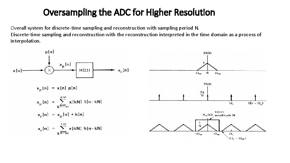
Oversampling the ADC for Higher Resolution Overall system for discrete-time sampling and reconstruction with sampling period N. Discrete-time sampling and reconstruction with the reconstruction interpreted in the time domain as a process of interpolation.

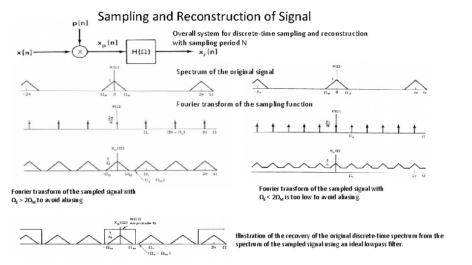
Sampling and Reconstruction of Signal Overall system for discrete-time sampling and reconstruction with sampling period N Spectrum of the original signal Fourier transform of the sampling function Fourier transform of the sampled signal with ΩS > 2ΩM to avoid aliasing Fourier transform of the sampled signal with ΩS < 2ΩM is too low to avoid aliasing. Illustration of the recovery of the original discrete-time spectrum from the spectrum of the sampled signal using an ideal lowpass filter.

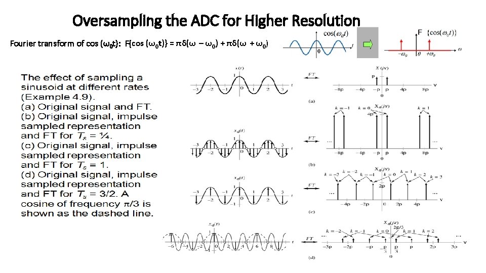
Oversampling the ADC for Higher Resolution Fourier transform of cos (ω0 t): F{cos (ω0 t)} = πδ(ω – ω0) + πδ(ω + ω0)

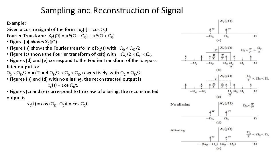
Sampling and Reconstruction of Signal Example: Given a cosine signal of the form: x. C(t) = cos Ω 0 t Fourier Transform: XC(jΩ) = πδ(Ω − Ω 0) + πδ(Ω + Ω 0) • Figure (a) shows XC(jΩ). • Figure (b) shows the Fourier transform of x. S(t) with Ω 0 < ΩS /2. • Figure (c) shows the Fourier transform of xs(t) with ΩS /2 < Ω 0 < ΩS. • Figures (d) and (e) correspond to the Fourier transform of the lowpass filter output for Ω 0 < ΩS /2 = π/T and ΩS /2 < Ω 0 < ΩS, respectively, with ΩC = ΩS /2. • Figures (b) and (d) with no aliasing, the reconstructed output is x. C(t) = cos Ω 0 t. • Figures (c) and (e) correspond to the case of aliasing, the reconstructed output is x. C(t) = cos (ΩS - Ω 0)t ≠ cos Ω 0 t.

References: Electronic Devices 9 th Edition by Thomas Floyd file: ///C: /Users/test 1/Downloads/slaa 323. pdf http: //www. atmel. com/images/doc 8003. pdf http: //www. analog. com/media/en/training-seminars/design-handbooks/Data-Conversion-Handbook/Chapter 8. pdf https: //www. physik. uni-kl. de/fileadmin/beigang/Vorlesungen/WS_07_08/Fourier_Transforms_Rick_Trebino. pdf web. engr. oregonstate. edu/~thinhq/teaching/ece 352/spring 07/ch 4 b. ppt ume. gatech. edu/mechatronics_course/DAC_S 05. ppt http: //www. analog. com/media/en/training-seminars/design-handbooks/Data-Conversion-Handbook/Chapter 5. pdf http: //www. analog. com/static/imported-files/tutorials/MT-003. pdf http: //www. hit. bme. hu/~papay/edu/Acrobat/Data. Conv. pdf Evaluating High Speed DAC Performance by Walt Kester – Analog Devices MT-013 Tutorial http: //www. ni. com/white-paper/4806/en/ Home > Products and Services > White Papers > Understanding Resolution in High-Speed Digitizers/Oscilloscopes http: //inst. eecs. berkeley. edu/~ee 247/fa 10/files 07/lectures/L 11_2_f 10. pdf http: //194. 81. 104. 27/~brian/DSP/ADC_notes. pdf ume. gatech. edu/mechatronics_course/ADC_F 10. pptx https: //inst. eecs. berkeley. edu/~ee 247/fa 07/lectures. html http: //control. ucsd. edu/mauricio/courses/mae 143 a/lectures/8 sampling. pdf http: //www. maximintegrated. com/en/app-notes/index. mvp/id/1041 http: //users. ece. utexas. edu/~bevans/courses/ee 313/lectures/16_Sampling_Theorem/lecture 16. ppt http: //nptel. ac. in/courses/112103174/module 2/lec 8/2. html http: //www. electronics-tutorial. net/analog-integrated-circuits/data-converters/dual-slope-type-adc/ http: //www. asdlib. org/online. Articles/elabware/Scheeline_ADC/ADC_V 2 F. html

References: www. ti. com/lit/an/slaa 587. pdf 1. Understanding Data Converters – SLAA 013 2. ADS 8318 data sheet – SLAS 568 A http: //citeseerx. ist. psu. edu/viewdoc/download; jsessionid=98 D 88 A 3076 BBB 49 FAD 450352 ABDA 637 E? doi=10. 1. 1. 130. 7043&rep=rep 1&type=pdf www. skillbank. co. uk/Signal. Conversion/index. htm http: //164. 100. 133. 129: 81/e. CONTENT/Uploads/session_06_Introduction%20 to%20 Data%20 Converter. pdf http: //masteringelectronicsdesign. com/an-adc-and-dac-least-significant-bit-lsb/ http: //www. analog. com/static/imported-files/tutorials/MT-003. pdf https: //inst. eecs. berkeley. edu/~ee 247/fa 07/files 07/lectures/L 12_f 07. pdf http: //www. ecircuitcenter. com/Circuits/DVM/dual_slope_int 1. htm http: //www. hit. bme. hu/~papay/edu/Acrobat/Data. Conv. pdf http: //masteringelectronicsdesign. com/an-adc-and-dac-integral-non-linearity-inl/ Evaluating High Speed DAC Performance by Walt Kester – Analog Devices MT-013 Tutorial https: //inst. eecs. berkeley. edu/~ee 247/fa 07/lectures. html http: //www. dspguide. com/ch 3/1. htm http: //www. cse. psu. edu/~chip/course/analog/lecture/SFDR 1. pdf http: //www. cypress. com/file/144536/download http: //www. atx 7006. com/articles/static_analysis/dac#gain_error https: //www. maximintegrated. com/en/app-notes/index. mvp/id/641 http: //blog. prosig. com/2008/04/14/what-is-db-noise-floor-dynamic-range/

References: http: //194. 81. 104. 27/~brian/DSP/ADC_notes. pdf http: //ume. gatech. edu/mechatronics_course/ADC_F 08. pdf http: //astro. temple. edu/~silage/Chapter 8 MS. pdf http: //www. embedded. com/design/configurable-systems/4025078/Understanding-analog-to-digital-converterspecifications ume. gatech. edu/mechatronics_course/ADC_F 12. pptx http: //www. elin. ttu. ee/~olev/lect 2. pdf http: //my. ece. msstate. edu/faculty/reese/ece 3724_pic 16/lectures/adcdac. pdf http: //www. mediacollege. com/glossary/q/quantization. html http: //www. ti. com/lit/an/slaa 013. pdf http: //www. ti. com/europe/downloads/Key%20 Parameters. pdf https: //courses. engr. illinois. edu/ece 110/content/course. Notes/files/? sampling. And. Quantization http: //www. onmyphd. com/? p=quantization. noise. snr http: //ecetutorials. com/digital-electronics/data-converters-dac-or-adc/