Introduction to CMOS VLSI Design Lecture 25 Package

- Slides: 36

Introduction to CMOS VLSI Design Lecture 25: Package, Power, Clock, and I/O David Harris 25: Package, Power, and I/O Harvey Mudd College Spring 2007 1

Outline q q Packaging Power Distribution Clock Distribution I/O 25: Package, Power, and I/O CMOS VLSI Design 2

Packages q Package functions – Electrical connection of signals and power from chip to board – Little delay or distortion – Mechanical connection of chip to board – Removes heat produced on chip – Protects chip from mechanical damage – Compatible with thermal expansion – Inexpensive to manufacture and test 25: Package, Power, and I/O CMOS VLSI Design 3

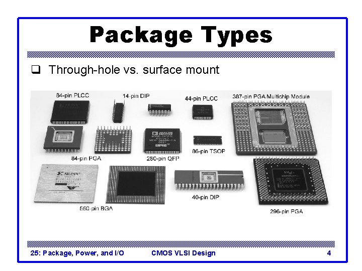
Package Types q Through-hole vs. surface mount 25: Package, Power, and I/O CMOS VLSI Design 4

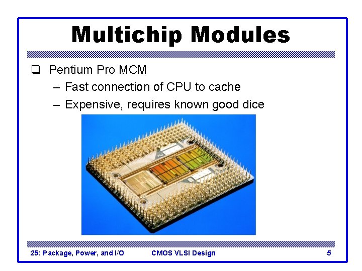
Multichip Modules q Pentium Pro MCM – Fast connection of CPU to cache – Expensive, requires known good dice 25: Package, Power, and I/O CMOS VLSI Design 5

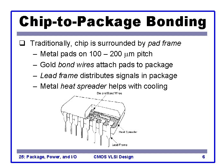
Chip-to-Package Bonding q Traditionally, chip is surrounded by pad frame – Metal pads on 100 – 200 mm pitch – Gold bond wires attach pads to package – Lead frame distributes signals in package – Metal heat spreader helps with cooling 25: Package, Power, and I/O CMOS VLSI Design 6

Advanced Packages q Bond wires contribute parasitic inductance q Fancy packages have many signal, power layers – Like tiny printed circuit boards q Flip-chip places connections across surface of die rather than around periphery – Top level metal pads covered with solder balls – Chip flips upside down – Carefully aligned to package (done blind!) – Heated to melt balls – Also called C 4 (Controlled Collapse Chip Connection) 25: Package, Power, and I/O CMOS VLSI Design 7

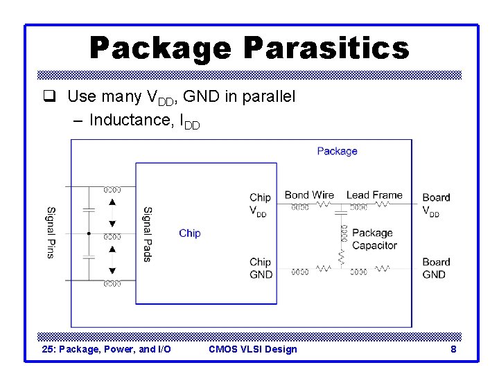
Package Parasitics q Use many VDD, GND in parallel – Inductance, IDD 25: Package, Power, and I/O CMOS VLSI Design 8

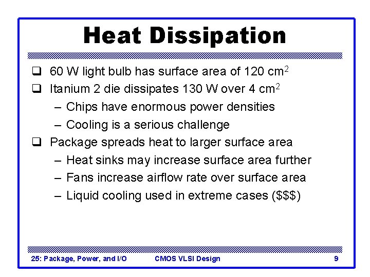
Heat Dissipation q 60 W light bulb has surface area of 120 cm 2 q Itanium 2 die dissipates 130 W over 4 cm 2 – Chips have enormous power densities – Cooling is a serious challenge q Package spreads heat to larger surface area – Heat sinks may increase surface area further – Fans increase airflow rate over surface area – Liquid cooling used in extreme cases ($$$) 25: Package, Power, and I/O CMOS VLSI Design 9

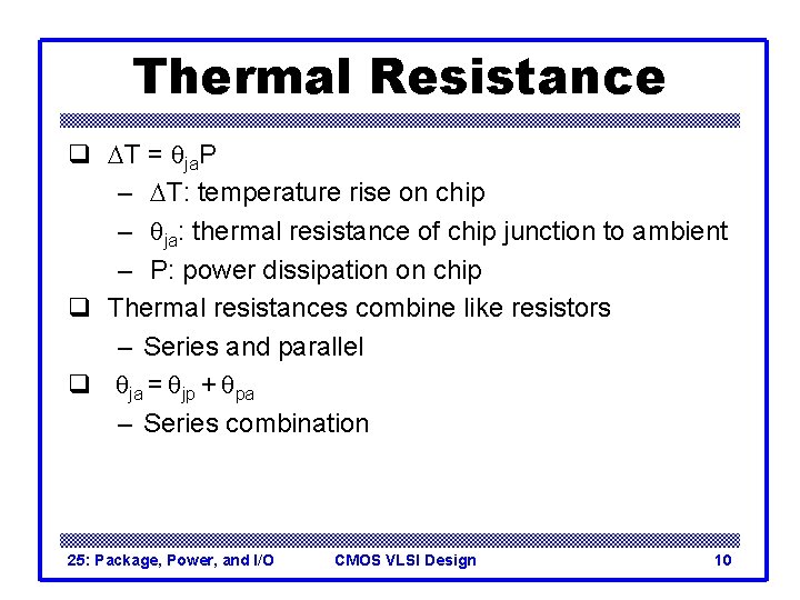
Thermal Resistance q DT = qja. P – DT: temperature rise on chip – qja: thermal resistance of chip junction to ambient – P: power dissipation on chip q Thermal resistances combine like resistors – Series and parallel q qja = qjp + qpa – Series combination 25: Package, Power, and I/O CMOS VLSI Design 10

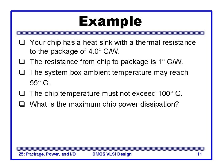
Example q Your chip has a heat sink with a thermal resistance to the package of 4. 0° C/W. q The resistance from chip to package is 1° C/W. q The system box ambient temperature may reach 55° C. q The chip temperature must not exceed 100° C. q What is the maximum chip power dissipation? 25: Package, Power, and I/O CMOS VLSI Design 11

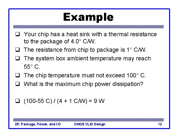
Example q Your chip has a heat sink with a thermal resistance to the package of 4. 0° C/W. q The resistance from chip to package is 1° C/W. q The system box ambient temperature may reach 55° C. q The chip temperature must not exceed 100° C. q What is the maximum chip power dissipation? q (100 -55 C) / (4 + 1 C/W) = 9 W 25: Package, Power, and I/O CMOS VLSI Design 12

Power Distribution q Power Distribution Network functions – Carry current from pads to transistors on chip – Maintain stable voltage with low noise – Provide average and peak power demands – Provide current return paths for signals – Avoid electromigration & self-heating wearout – Consume little chip area and wire – Easy to lay out 25: Package, Power, and I/O CMOS VLSI Design 13

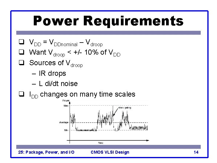
Power Requirements q VDD = VDDnominal – Vdroop q Want Vdroop < +/- 10% of VDD q Sources of Vdroop – IR drops – L di/dt noise q IDD changes on many time scales 25: Package, Power, and I/O CMOS VLSI Design 14

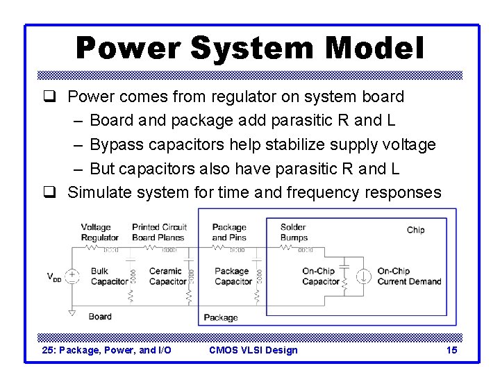
Power System Model q Power comes from regulator on system board – Board and package add parasitic R and L – Bypass capacitors help stabilize supply voltage – But capacitors also have parasitic R and L q Simulate system for time and frequency responses 25: Package, Power, and I/O CMOS VLSI Design 15

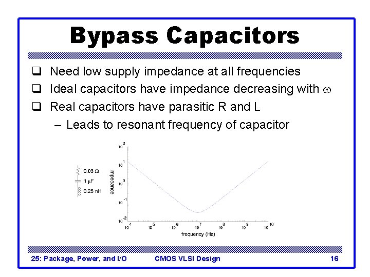
Bypass Capacitors q Need low supply impedance at all frequencies q Ideal capacitors have impedance decreasing with w q Real capacitors have parasitic R and L – Leads to resonant frequency of capacitor 25: Package, Power, and I/O CMOS VLSI Design 16

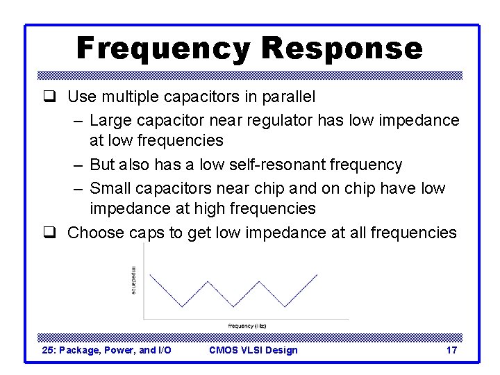
Frequency Response q Use multiple capacitors in parallel – Large capacitor near regulator has low impedance at low frequencies – But also has a low self-resonant frequency – Small capacitors near chip and on chip have low impedance at high frequencies q Choose caps to get low impedance at all frequencies 25: Package, Power, and I/O CMOS VLSI Design 17

Clock Distribution q On a small chip, the clock distribution network is just a wire – And possibly an inverter for clkb q On practical chips, the RC delay of the wire resistance and gate load is very long – Variations in this delay cause clock to get to different elements at different times – This is called clock skew q Most chips use repeaters to buffer the clock and equalize the delay – Reduces but doesn’t eliminate skew 25: Package, Power, and I/O CMOS VLSI Design 18

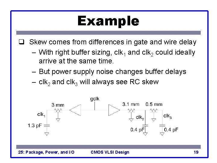
Example q Skew comes from differences in gate and wire delay – With right buffer sizing, clk 1 and clk 2 could ideally arrive at the same time. – But power supply noise changes buffer delays – clk 2 and clk 3 will always see RC skew 25: Package, Power, and I/O CMOS VLSI Design 19

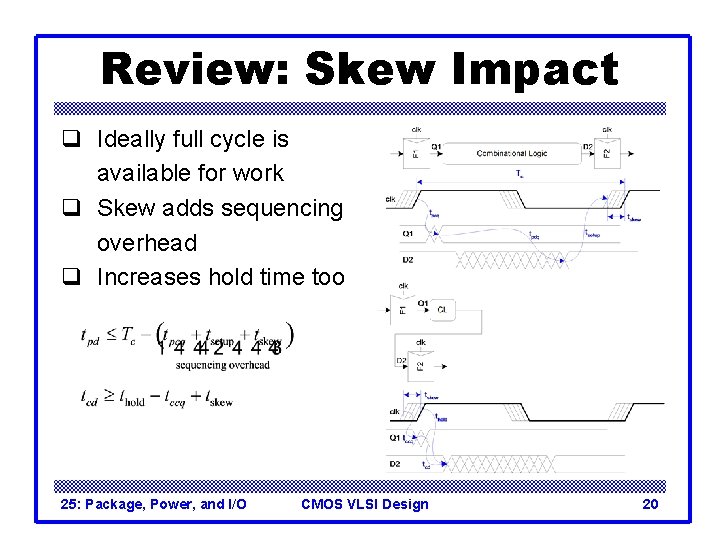
Review: Skew Impact q Ideally full cycle is available for work q Skew adds sequencing overhead q Increases hold time too 25: Package, Power, and I/O CMOS VLSI Design 20

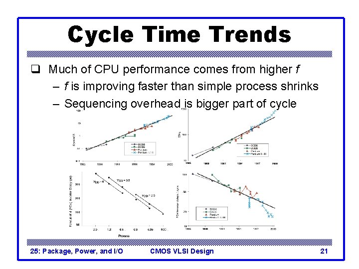
Cycle Time Trends q Much of CPU performance comes from higher f – f is improving faster than simple process shrinks – Sequencing overhead is bigger part of cycle 25: Package, Power, and I/O CMOS VLSI Design 21

Solutions q Reduce clock skew – Careful clock distribution network design – Plenty of metal wiring resources q Analyze clock skew – Only budget actual, not worst case skews – Local vs. global skew budgets q Tolerate clock skew – Choose circuit structures insensitive to skew 25: Package, Power, and I/O CMOS VLSI Design 22

Clock Dist. Networks q q Ad hoc Grids H-tree Hybrid 25: Package, Power, and I/O CMOS VLSI Design 23

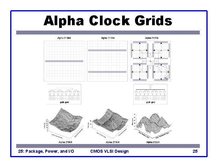
Clock Grids q q Use grid on two or more levels to carry clock Make wires wide to reduce RC delay Ensures low skew between nearby points But possibly large skew across die 25: Package, Power, and I/O CMOS VLSI Design 24

Alpha Clock Grids 25: Package, Power, and I/O CMOS VLSI Design 25

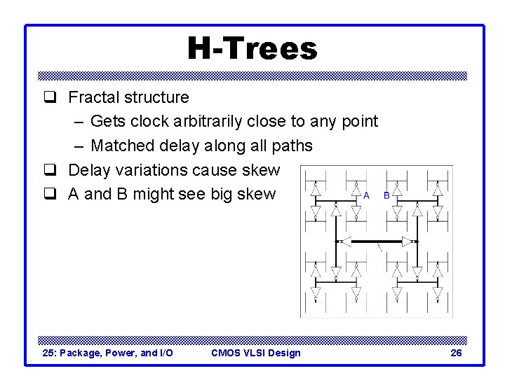
H-Trees q Fractal structure – Gets clock arbitrarily close to any point – Matched delay along all paths q Delay variations cause skew q A and B might see big skew 25: Package, Power, and I/O CMOS VLSI Design 26

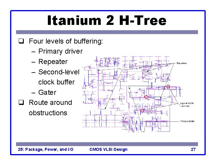
Itanium 2 H-Tree q Four levels of buffering: – Primary driver – Repeater – Second-level clock buffer – Gater q Route around obstructions 25: Package, Power, and I/O CMOS VLSI Design 27

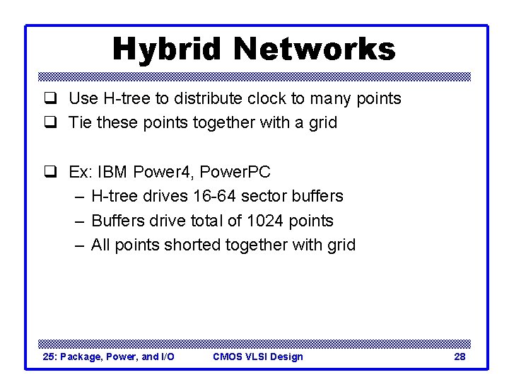
Hybrid Networks q Use H-tree to distribute clock to many points q Tie these points together with a grid q Ex: IBM Power 4, Power. PC – H-tree drives 16 -64 sector buffers – Buffers drive total of 1024 points – All points shorted together with grid 25: Package, Power, and I/O CMOS VLSI Design 28

Input / Output q Input/Output System functions – Communicate between chip and external world – Drive large capacitance off chip – Operate at compatible voltage levels – Provide adequate bandwidth – Limit slew rates to control di/dt noise – Protect chip against electrostatic discharge – Use small number of pins (low cost) 25: Package, Power, and I/O CMOS VLSI Design 29

I/O Pad Design q Pad types – VDD / GND – Output – Input – Bidirectional – Analog 25: Package, Power, and I/O CMOS VLSI Design 30

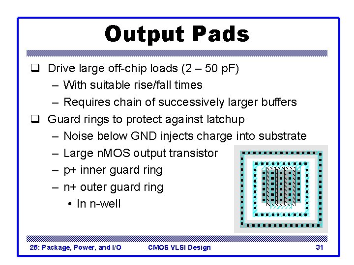
Output Pads q Drive large off-chip loads (2 – 50 p. F) – With suitable rise/fall times – Requires chain of successively larger buffers q Guard rings to protect against latchup – Noise below GND injects charge into substrate – Large n. MOS output transistor – p+ inner guard ring – n+ outer guard ring • In n-well 25: Package, Power, and I/O CMOS VLSI Design 31

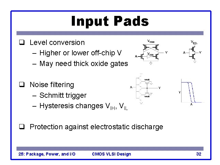
Input Pads q Level conversion – Higher or lower off-chip V – May need thick oxide gates q Noise filtering – Schmitt trigger – Hysteresis changes VIH, VIL q Protection against electrostatic discharge 25: Package, Power, and I/O CMOS VLSI Design 32

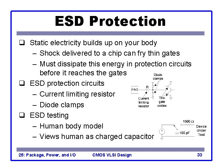
ESD Protection q Static electricity builds up on your body – Shock delivered to a chip can fry thin gates – Must dissipate this energy in protection circuits before it reaches the gates q ESD protection circuits – Current limiting resistor – Diode clamps q ESD testing – Human body model – Views human as charged capacitor 25: Package, Power, and I/O CMOS VLSI Design 33

Bidirectional Pads q Combine input and output pad q Need tristate driver on output – Use enable signal to set direction – Optimized tristate avoids huge series transistors 25: Package, Power, and I/O CMOS VLSI Design 34

Analog Pads q Pass analog voltages directly in or out of chip – No buffering – Protection circuits must not distort voltages 25: Package, Power, and I/O CMOS VLSI Design 35

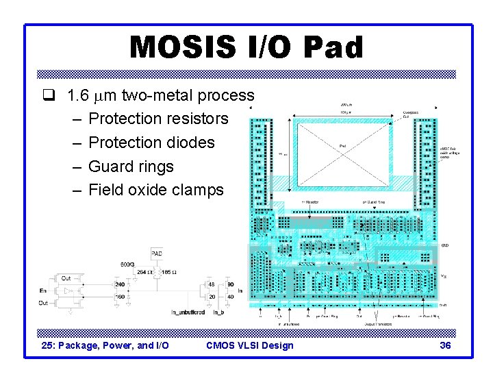
MOSIS I/O Pad q 1. 6 mm two-metal process – Protection resistors – Protection diodes – Guard rings – Field oxide clamps 25: Package, Power, and I/O CMOS VLSI Design 36