Introduction to CMOS VLSI Design Lecture 21 Scaling












- Slides: 61

Introduction to CMOS VLSI Design Lecture 21: Scaling and Economics David Harris 21: Scaling and Economics Harvey Mudd College Spring 2004 1

Outline q Scaling – Transistors – Interconnect – Future Challenges q VLSI Economics 21: Scaling and Economics CMOS VLSI Design 2

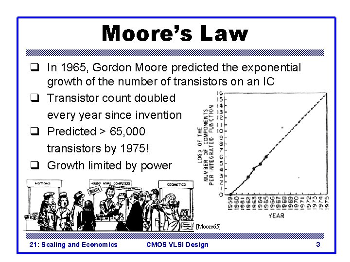
Moore’s Law q In 1965, Gordon Moore predicted the exponential growth of the number of transistors on an IC q Transistor count doubled every year since invention q Predicted > 65, 000 transistors by 1975! q Growth limited by power [Moore 65] 21: Scaling and Economics CMOS VLSI Design 3

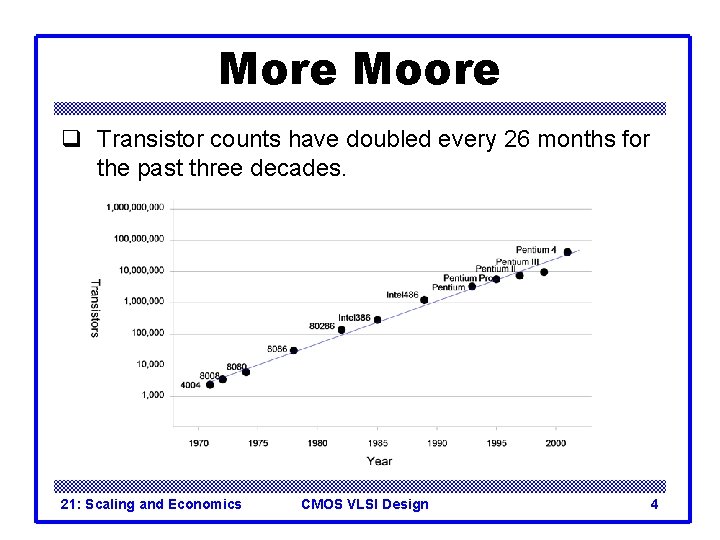
More Moore q Transistor counts have doubled every 26 months for the past three decades. 21: Scaling and Economics CMOS VLSI Design 4

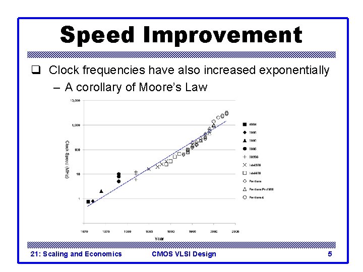
Speed Improvement q Clock frequencies have also increased exponentially – A corollary of Moore’s Law 21: Scaling and Economics CMOS VLSI Design 5

Why? q Why more transistors per IC? q Why faster computers? 21: Scaling and Economics CMOS VLSI Design 6

Why? q Why more transistors per IC? – Smaller transistors – Larger dice q Why faster computers? 21: Scaling and Economics CMOS VLSI Design 7

Why? q Why more transistors per IC? – Smaller transistors – Larger dice q Why faster computers? – Smaller, faster transistors – Better microarchitecture (more IPC) – Fewer gate delays per cycle 21: Scaling and Economics CMOS VLSI Design 8

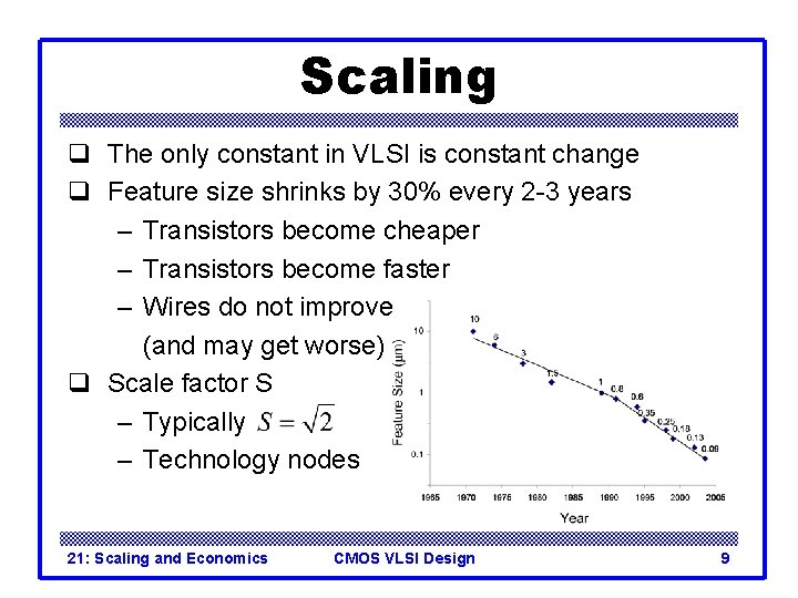
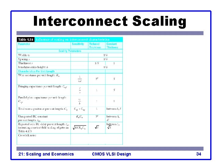
Scaling q The only constant in VLSI is constant change q Feature size shrinks by 30% every 2 -3 years – Transistors become cheaper – Transistors become faster – Wires do not improve (and may get worse) q Scale factor S – Typically – Technology nodes 21: Scaling and Economics CMOS VLSI Design 9

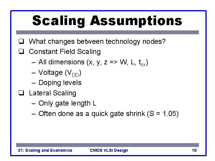
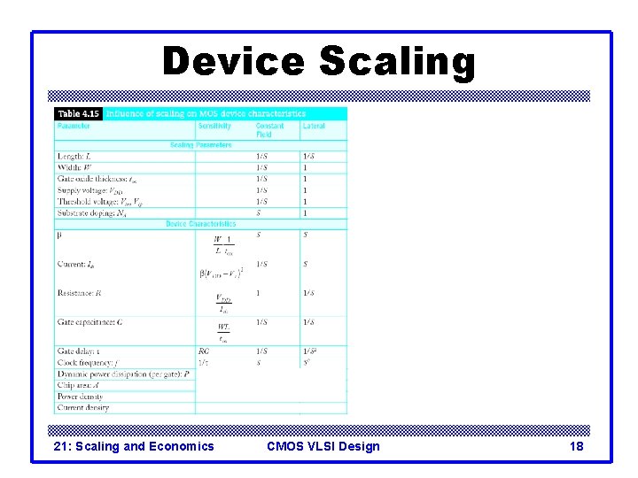
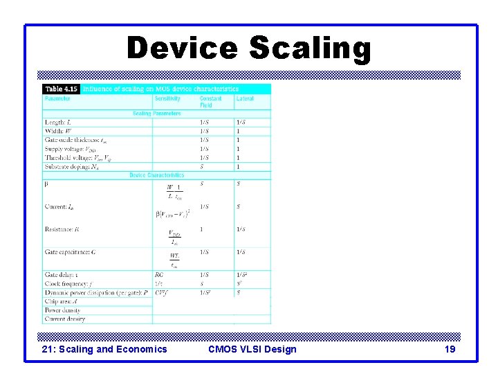
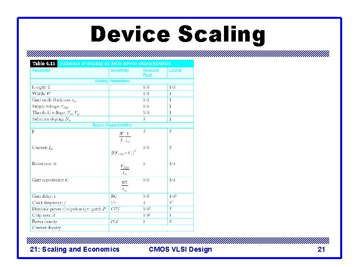
Scaling Assumptions q What changes between technology nodes? q Constant Field Scaling – All dimensions (x, y, z => W, L, tox) – Voltage (VDD) – Doping levels q Lateral Scaling – Only gate length L – Often done as a quick gate shrink (S = 1. 05) 21: Scaling and Economics CMOS VLSI Design 10

Device Scaling 21: Scaling and Economics CMOS VLSI Design 11

Device Scaling 21: Scaling and Economics CMOS VLSI Design 12

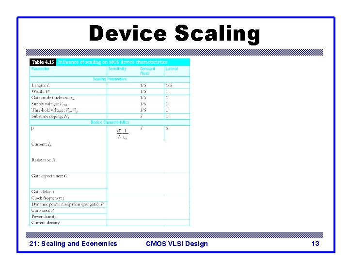
Device Scaling 21: Scaling and Economics CMOS VLSI Design 13

Device Scaling 21: Scaling and Economics CMOS VLSI Design 14

Device Scaling 21: Scaling and Economics CMOS VLSI Design 15

Device Scaling 21: Scaling and Economics CMOS VLSI Design 16

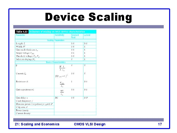
Device Scaling 21: Scaling and Economics CMOS VLSI Design 17

Device Scaling 21: Scaling and Economics CMOS VLSI Design 18

Device Scaling 21: Scaling and Economics CMOS VLSI Design 19

Device Scaling 21: Scaling and Economics CMOS VLSI Design 20

Device Scaling 21: Scaling and Economics CMOS VLSI Design 21

Device Scaling 21: Scaling and Economics CMOS VLSI Design 22

Observations q Gate capacitance per micron is nearly independent of process q But ON resistance * micron improves with process q Gates get faster with scaling (good) q Dynamic power goes down with scaling (good) q Current density goes up with scaling (bad) q Velocity saturation makes lateral scaling unsustainable 21: Scaling and Economics CMOS VLSI Design 23

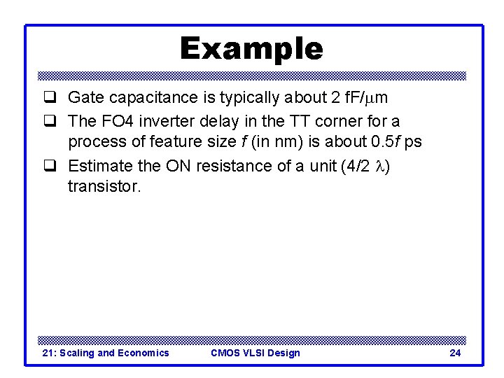
Example q Gate capacitance is typically about 2 f. F/mm q The FO 4 inverter delay in the TT corner for a process of feature size f (in nm) is about 0. 5 f ps q Estimate the ON resistance of a unit (4/2 l) transistor. 21: Scaling and Economics CMOS VLSI Design 24

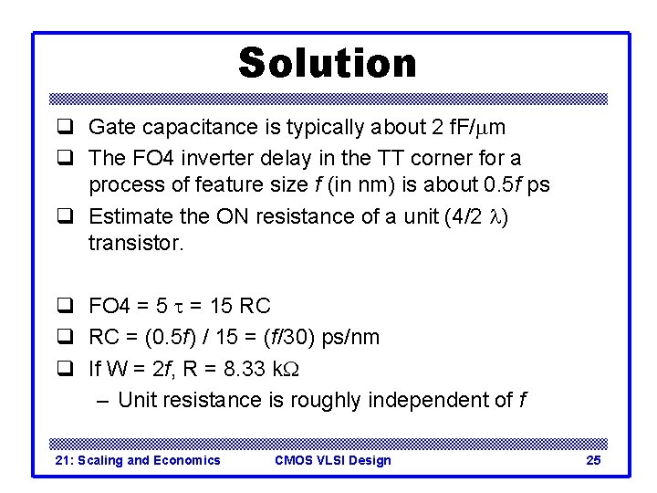
Solution q Gate capacitance is typically about 2 f. F/mm q The FO 4 inverter delay in the TT corner for a process of feature size f (in nm) is about 0. 5 f ps q Estimate the ON resistance of a unit (4/2 l) transistor. q FO 4 = 5 t = 15 RC q RC = (0. 5 f) / 15 = (f/30) ps/nm q If W = 2 f, R = 8. 33 k. W – Unit resistance is roughly independent of f 21: Scaling and Economics CMOS VLSI Design 25

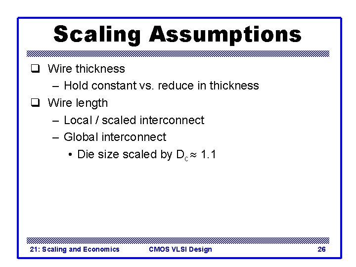
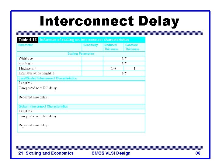
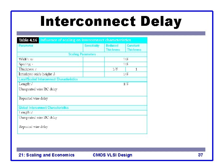
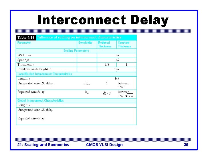
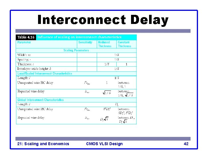
Scaling Assumptions q Wire thickness – Hold constant vs. reduce in thickness q Wire length – Local / scaled interconnect – Global interconnect • Die size scaled by Dc 1. 1 21: Scaling and Economics CMOS VLSI Design 26

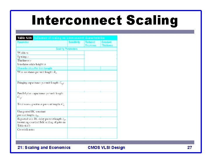
Interconnect Scaling 21: Scaling and Economics CMOS VLSI Design 27

Interconnect Scaling 21: Scaling and Economics CMOS VLSI Design 28

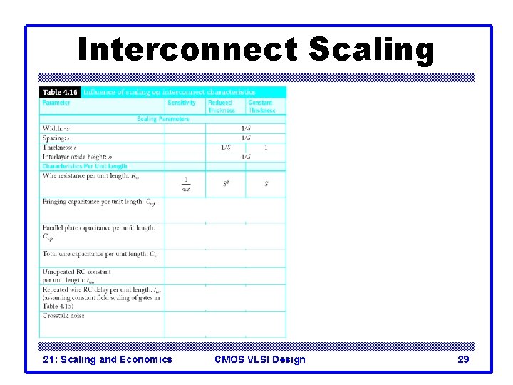
Interconnect Scaling 21: Scaling and Economics CMOS VLSI Design 29

Interconnect Scaling 21: Scaling and Economics CMOS VLSI Design 30

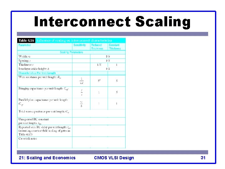
Interconnect Scaling 21: Scaling and Economics CMOS VLSI Design 31

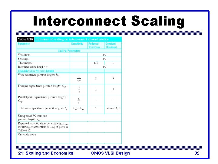
Interconnect Scaling 21: Scaling and Economics CMOS VLSI Design 32

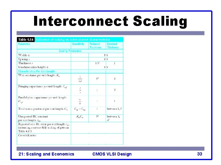
Interconnect Scaling 21: Scaling and Economics CMOS VLSI Design 33

Interconnect Scaling 21: Scaling and Economics CMOS VLSI Design 34

Interconnect Scaling 21: Scaling and Economics CMOS VLSI Design 35

Interconnect Delay 21: Scaling and Economics CMOS VLSI Design 36

Interconnect Delay 21: Scaling and Economics CMOS VLSI Design 37

Interconnect Delay 21: Scaling and Economics CMOS VLSI Design 38

Interconnect Delay 21: Scaling and Economics CMOS VLSI Design 39

Interconnect Delay 21: Scaling and Economics CMOS VLSI Design 40

Interconnect Delay 21: Scaling and Economics CMOS VLSI Design 41

Interconnect Delay 21: Scaling and Economics CMOS VLSI Design 42

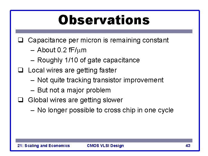
Observations q Capacitance per micron is remaining constant – About 0. 2 f. F/mm – Roughly 1/10 of gate capacitance q Local wires are getting faster – Not quite tracking transistor improvement – But not a major problem q Global wires are getting slower – No longer possible to cross chip in one cycle 21: Scaling and Economics CMOS VLSI Design 43

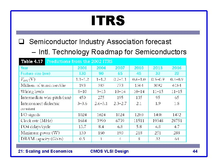
ITRS q Semiconductor Industry Association forecast – Intl. Technology Roadmap for Semiconductors 21: Scaling and Economics CMOS VLSI Design 44

Scaling Implications q q q Improved Performance Improved Cost Interconnect Woes Power Woes Productivity Challenges Physical Limits 21: Scaling and Economics CMOS VLSI Design 45

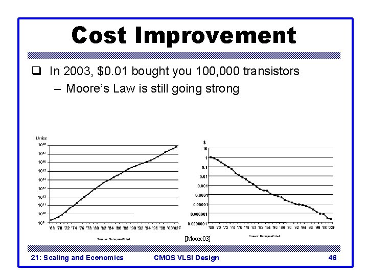
Cost Improvement q In 2003, $0. 01 bought you 100, 000 transistors – Moore’s Law is still going strong [Moore 03] 21: Scaling and Economics CMOS VLSI Design 46

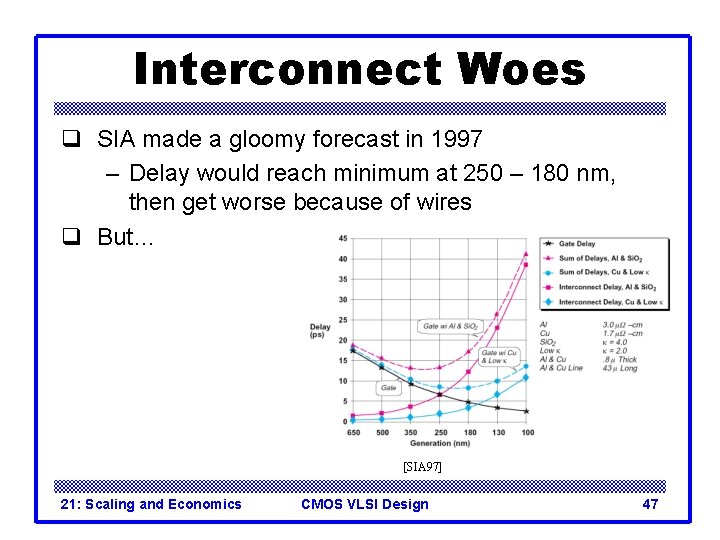
Interconnect Woes q SIA made a gloomy forecast in 1997 – Delay would reach minimum at 250 – 180 nm, then get worse because of wires q But… [SIA 97] 21: Scaling and Economics CMOS VLSI Design 47

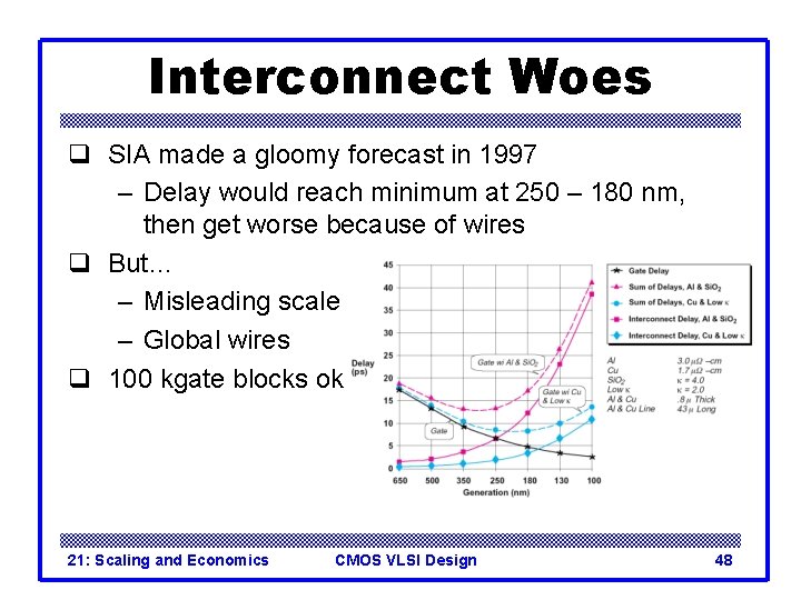
Interconnect Woes q SIA made a gloomy forecast in 1997 – Delay would reach minimum at 250 – 180 nm, then get worse because of wires q But… – Misleading scale – Global wires q 100 kgate blocks ok 21: Scaling and Economics CMOS VLSI Design 48

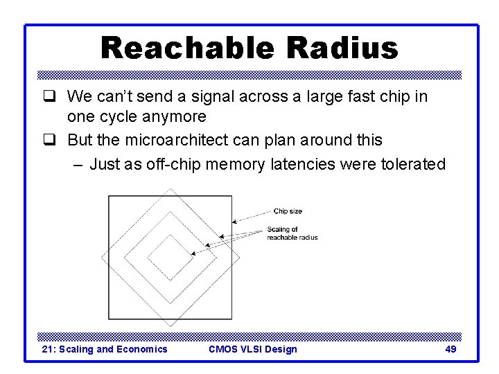
Reachable Radius q We can’t send a signal across a large fast chip in one cycle anymore q But the microarchitect can plan around this – Just as off-chip memory latencies were tolerated 21: Scaling and Economics CMOS VLSI Design 49

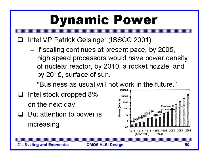
Dynamic Power q Intel VP Patrick Gelsinger (ISSCC 2001) – If scaling continues at present pace, by 2005, high speed processors would have power density of nuclear reactor, by 2010, a rocket nozzle, and by 2015, surface of sun. – “Business as usual will not work in the future. ” q Intel stock dropped 8% on the next day q But attention to power is increasing [Moore 03] 21: Scaling and Economics CMOS VLSI Design 50

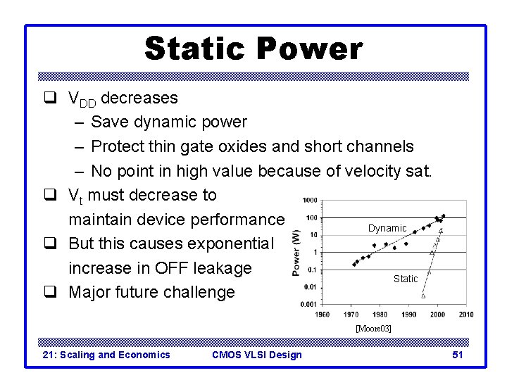
Static Power q VDD decreases – Save dynamic power – Protect thin gate oxides and short channels – No point in high value because of velocity sat. q Vt must decrease to maintain device performance Dynamic q But this causes exponential increase in OFF leakage Static q Major future challenge [Moore 03] 21: Scaling and Economics CMOS VLSI Design 51

Productivity q Transistor count is increasing faster than designer productivity (gates / week) – Bigger design teams • Up to 500 for a high-end microprocessor – More expensive design cost – Pressure to raise productivity • Rely on synthesis, IP blocks – Need for good engineering managers 21: Scaling and Economics CMOS VLSI Design 52

Physical Limits q Will Moore’s Law run out of steam? – Can’t build transistors smaller than an atom… q Many reasons have been predicted for end of scaling – Dynamic power – Subthreshold leakage, tunneling – Short channel effects – Fabrication costs – Electromigration – Interconnect delay q Rumors of demise have been exaggerated 21: Scaling and Economics CMOS VLSI Design 53

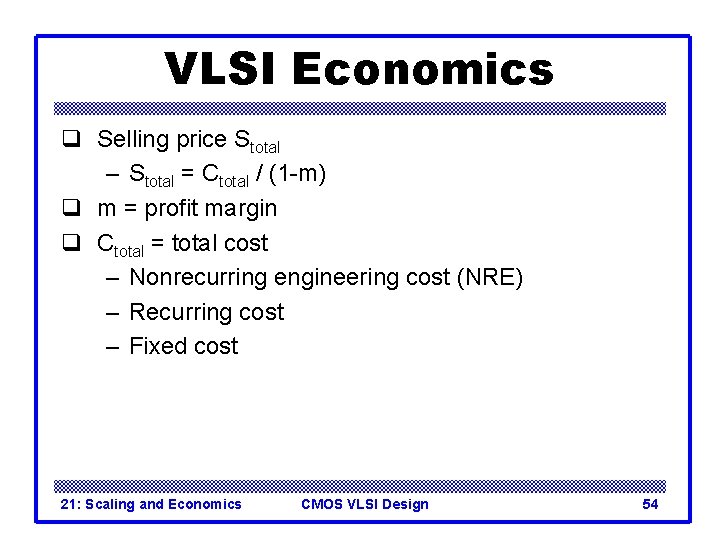
VLSI Economics q Selling price Stotal – Stotal = Ctotal / (1 -m) q m = profit margin q Ctotal = total cost – Nonrecurring engineering cost (NRE) – Recurring cost – Fixed cost 21: Scaling and Economics CMOS VLSI Design 54

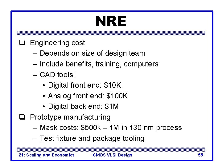
NRE q Engineering cost – Depends on size of design team – Include benefits, training, computers – CAD tools: • Digital front end: $10 K • Analog front end: $100 K • Digital back end: $1 M q Prototype manufacturing – Mask costs: $500 k – 1 M in 130 nm process – Test fixture and package tooling 21: Scaling and Economics CMOS VLSI Design 55

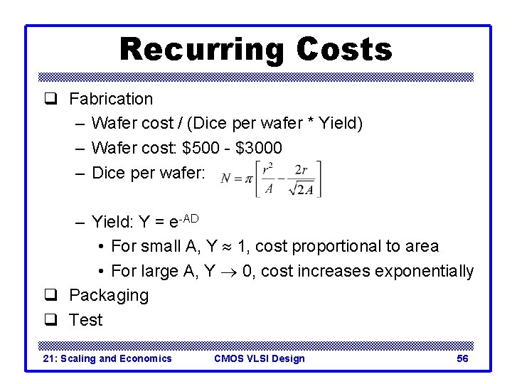
Recurring Costs q Fabrication – Wafer cost / (Dice per wafer * Yield) – Wafer cost: $500 - $3000 – Dice per wafer: – Yield: Y = e-AD • For small A, Y 1, cost proportional to area • For large A, Y 0, cost increases exponentially q Packaging q Test 21: Scaling and Economics CMOS VLSI Design 56

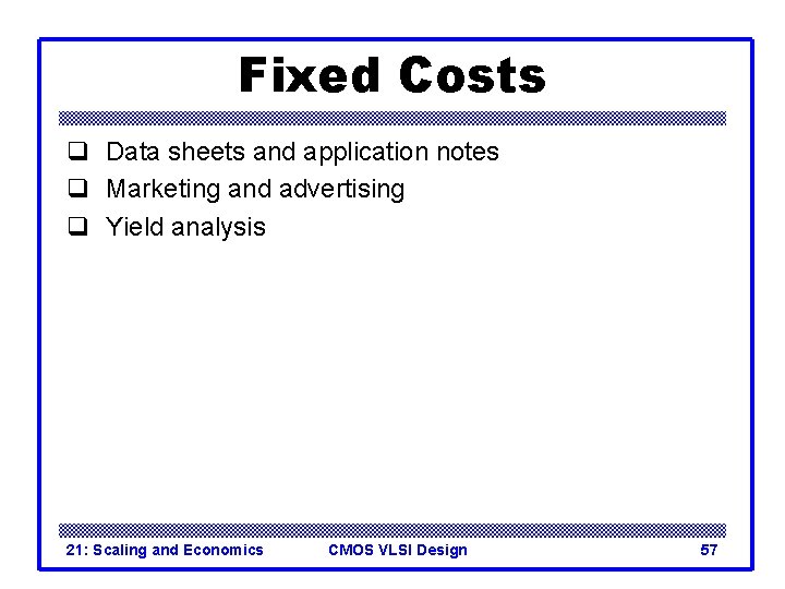
Fixed Costs q Data sheets and application notes q Marketing and advertising q Yield analysis 21: Scaling and Economics CMOS VLSI Design 57

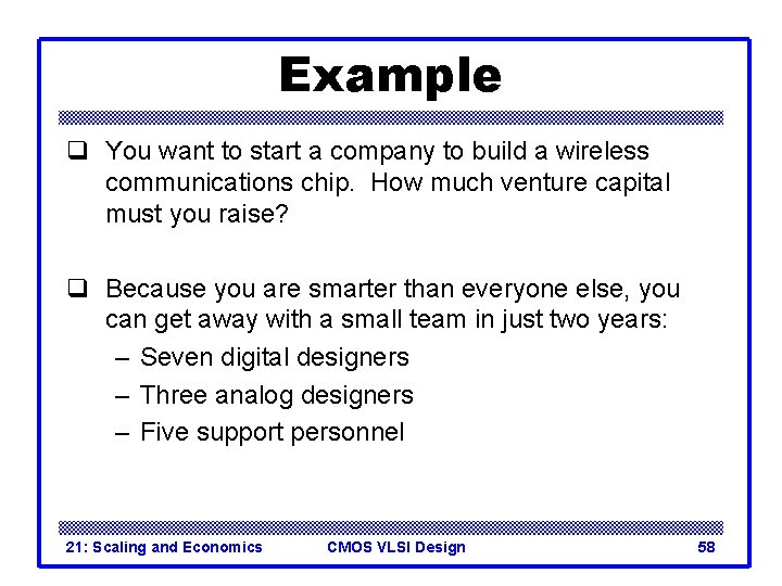
Example q You want to start a company to build a wireless communications chip. How much venture capital must you raise? q Because you are smarter than everyone else, you can get away with a small team in just two years: – Seven digital designers – Three analog designers – Five support personnel 21: Scaling and Economics CMOS VLSI Design 58

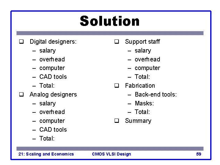
Solution q Digital designers: – salary – overhead – computer – CAD tools – Total: q Analog designers – salary – overhead – computer – CAD tools – Total: 21: Scaling and Economics q Support staff – salary – overhead – computer – Total: q Fabrication – Back-end tools: – Masks: – Total: q Summary CMOS VLSI Design 59

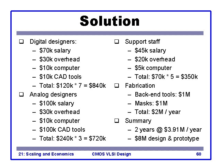
Solution q Digital designers: – $70 k salary – $30 k overhead – $10 k computer – $10 k CAD tools – Total: $120 k * 7 = $840 k q Analog designers – $100 k salary – $30 k overhead – $10 k computer – $100 k CAD tools – Total: $240 k * 3 = $720 k 21: Scaling and Economics q Support staff – $45 k salary – $20 k overhead – $5 k computer – Total: $70 k * 5 = $350 k q Fabrication – Back-end tools: $1 M – Masks: $1 M – Total: $2 M / year q Summary – 2 years @ $3. 91 M / year – $8 M design & prototype CMOS VLSI Design 60

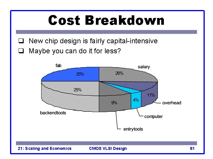
Cost Breakdown q New chip design is fairly capital-intensive q Maybe you can do it for less? 21: Scaling and Economics CMOS VLSI Design 61