Introduction to CMOS VLSI Design Lecture 18 Design
- Slides: 24

Introduction to CMOS VLSI Design Lecture 18: Design for Low Power David Harris 18: Design for Low Power Harvey Mudd College Spring 2004 1

Outline q q Power and Energy Dynamic Power Static Power Low Power Design 18: Design for Low Power CMOS VLSI Design 2

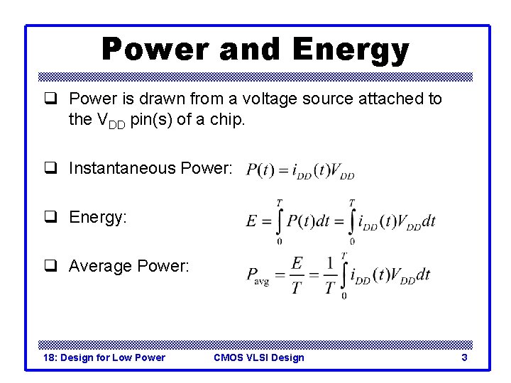
Power and Energy q Power is drawn from a voltage source attached to the VDD pin(s) of a chip. q Instantaneous Power: q Energy: q Average Power: 18: Design for Low Power CMOS VLSI Design 3

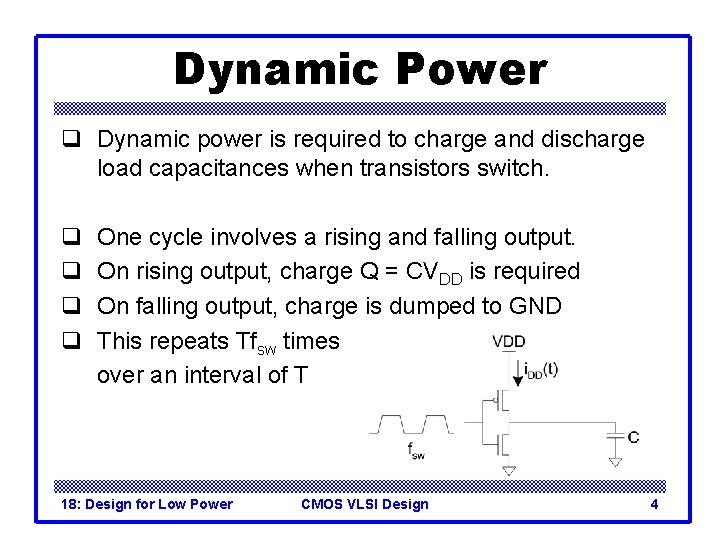
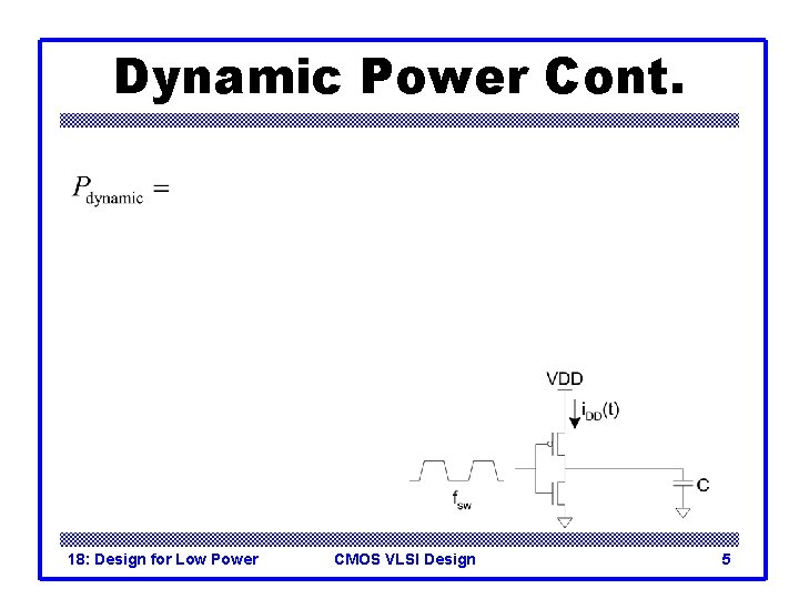
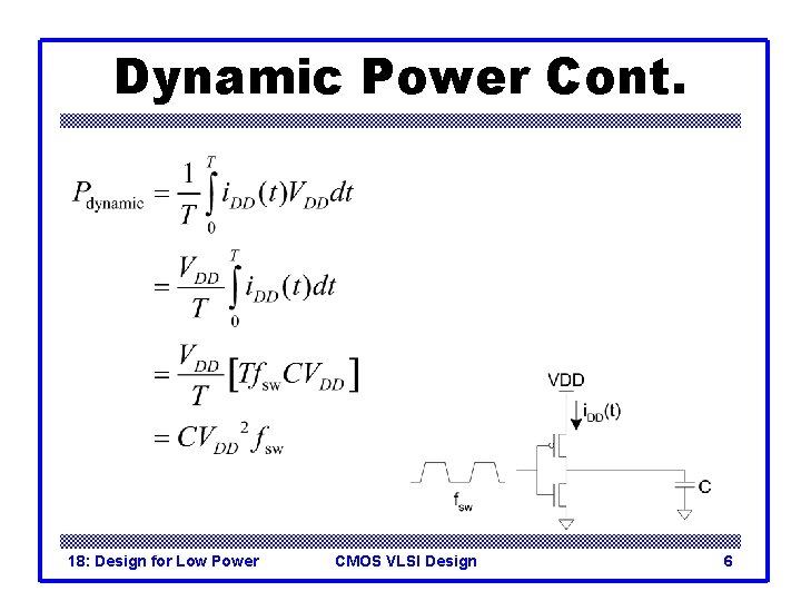
Dynamic Power q Dynamic power is required to charge and discharge load capacitances when transistors switch. q q One cycle involves a rising and falling output. On rising output, charge Q = CVDD is required On falling output, charge is dumped to GND This repeats Tfsw times over an interval of T 18: Design for Low Power CMOS VLSI Design 4

Dynamic Power Cont. 18: Design for Low Power CMOS VLSI Design 5

Dynamic Power Cont. 18: Design for Low Power CMOS VLSI Design 6

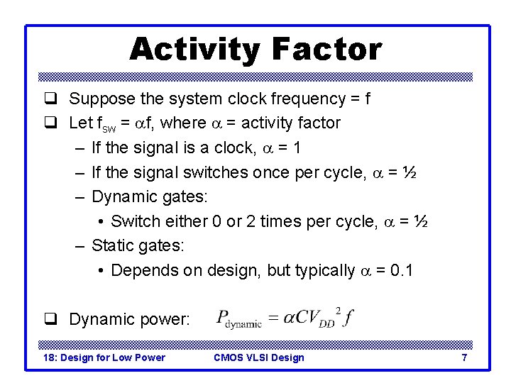
Activity Factor q Suppose the system clock frequency = f q Let fsw = af, where a = activity factor – If the signal is a clock, a = 1 – If the signal switches once per cycle, a = ½ – Dynamic gates: • Switch either 0 or 2 times per cycle, a = ½ – Static gates: • Depends on design, but typically a = 0. 1 q Dynamic power: 18: Design for Low Power CMOS VLSI Design 7

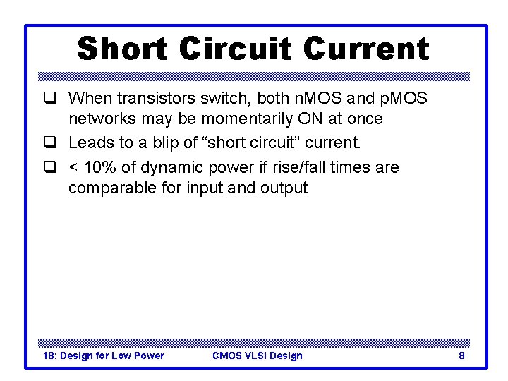
Short Circuit Current q When transistors switch, both n. MOS and p. MOS networks may be momentarily ON at once q Leads to a blip of “short circuit” current. q < 10% of dynamic power if rise/fall times are comparable for input and output 18: Design for Low Power CMOS VLSI Design 8

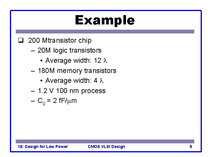
Example q 200 Mtransistor chip – 20 M logic transistors • Average width: 12 l – 180 M memory transistors • Average width: 4 l – 1. 2 V 100 nm process – Cg = 2 f. F/mm 18: Design for Low Power CMOS VLSI Design 9

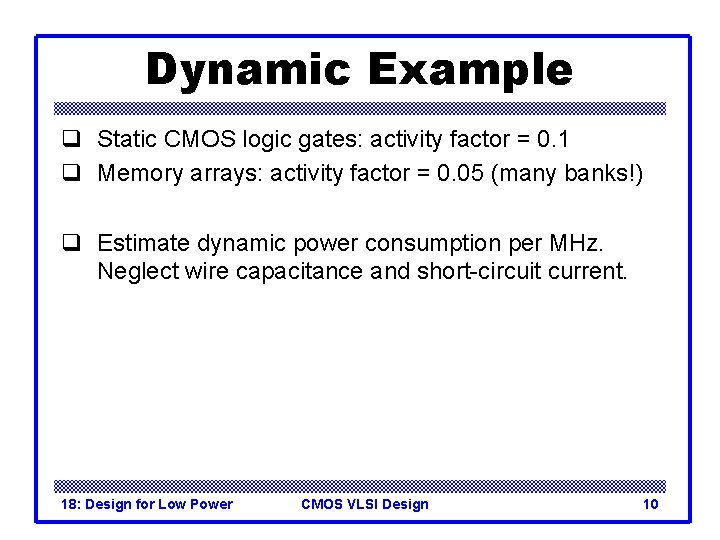
Dynamic Example q Static CMOS logic gates: activity factor = 0. 1 q Memory arrays: activity factor = 0. 05 (many banks!) q Estimate dynamic power consumption per MHz. Neglect wire capacitance and short-circuit current. 18: Design for Low Power CMOS VLSI Design 10

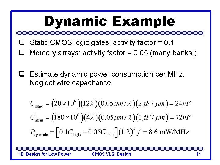
Dynamic Example q Static CMOS logic gates: activity factor = 0. 1 q Memory arrays: activity factor = 0. 05 (many banks!) q Estimate dynamic power consumption per MHz. Neglect wire capacitance. 18: Design for Low Power CMOS VLSI Design 11

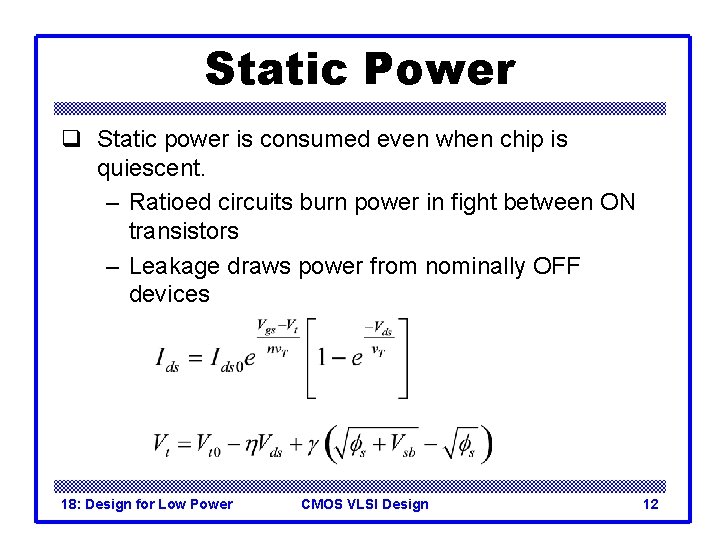
Static Power q Static power is consumed even when chip is quiescent. – Ratioed circuits burn power in fight between ON transistors – Leakage draws power from nominally OFF devices 18: Design for Low Power CMOS VLSI Design 12

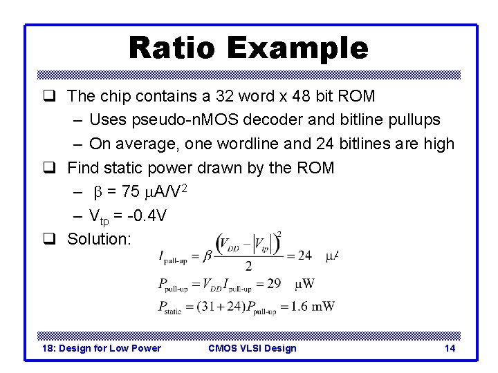
Ratio Example q The chip contains a 32 word x 48 bit ROM – Uses pseudo-n. MOS decoder and bitline pullups – On average, one wordline and 24 bitlines are high q Find static power drawn by the ROM – b = 75 m. A/V 2 – Vtp = -0. 4 V 18: Design for Low Power CMOS VLSI Design 13

Ratio Example q The chip contains a 32 word x 48 bit ROM – Uses pseudo-n. MOS decoder and bitline pullups – On average, one wordline and 24 bitlines are high q Find static power drawn by the ROM – b = 75 m. A/V 2 – Vtp = -0. 4 V q Solution: 18: Design for Low Power CMOS VLSI Design 14

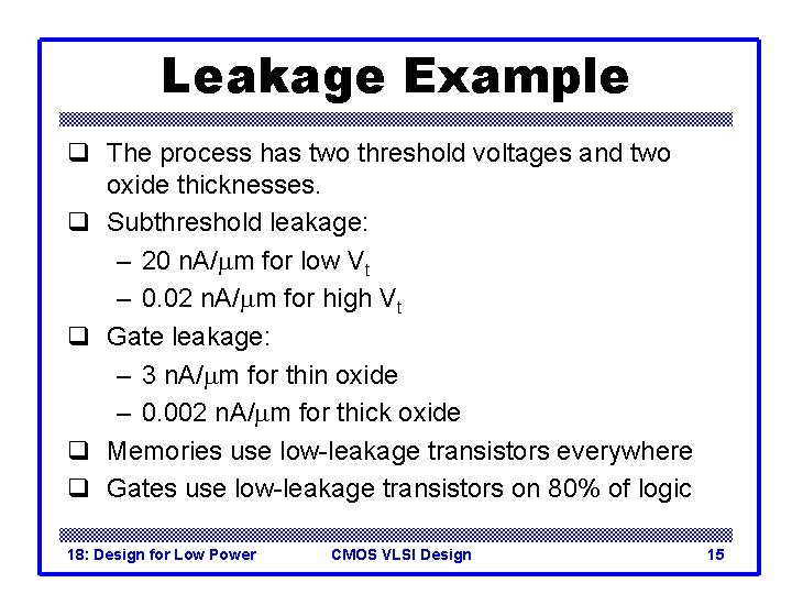
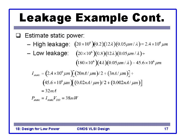
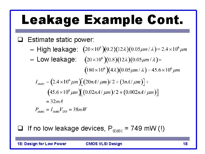
Leakage Example q The process has two threshold voltages and two oxide thicknesses. q Subthreshold leakage: – 20 n. A/mm for low Vt – 0. 02 n. A/mm for high Vt q Gate leakage: – 3 n. A/mm for thin oxide – 0. 002 n. A/mm for thick oxide q Memories use low-leakage transistors everywhere q Gates use low-leakage transistors on 80% of logic 18: Design for Low Power CMOS VLSI Design 15

Leakage Example Cont. q Estimate static power: 18: Design for Low Power CMOS VLSI Design 16

Leakage Example Cont. q Estimate static power: – High leakage: – Low leakage: 18: Design for Low Power CMOS VLSI Design 17

Leakage Example Cont. q Estimate static power: – High leakage: – Low leakage: q If no low leakage devices, Pstatic = 749 m. W (!) 18: Design for Low Power CMOS VLSI Design 18

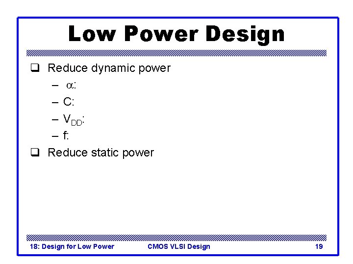
Low Power Design q Reduce dynamic power – a: – C: – VDD: – f: q Reduce static power 18: Design for Low Power CMOS VLSI Design 19

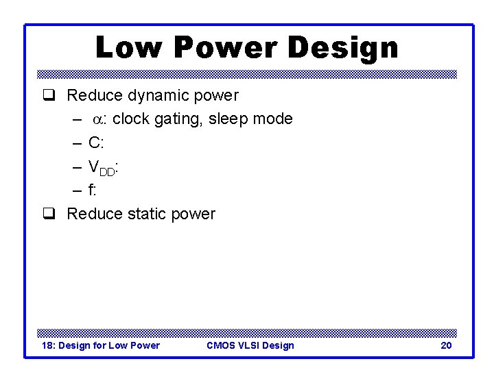
Low Power Design q Reduce dynamic power – a: clock gating, sleep mode – C: – VDD: – f: q Reduce static power 18: Design for Low Power CMOS VLSI Design 20

Low Power Design q Reduce dynamic power – a: clock gating, sleep mode – C: small transistors (esp. on clock), short wires – VDD: – f: q Reduce static power 18: Design for Low Power CMOS VLSI Design 21

Low Power Design q Reduce dynamic power – a: clock gating, sleep mode – C: small transistors (esp. on clock), short wires – VDD: lowest suitable voltage – f: q Reduce static power 18: Design for Low Power CMOS VLSI Design 22

Low Power Design q Reduce dynamic power – a: clock gating, sleep mode – C: small transistors (esp. on clock), short wires – VDD: lowest suitable voltage – f: lowest suitable frequency q Reduce static power 18: Design for Low Power CMOS VLSI Design 23

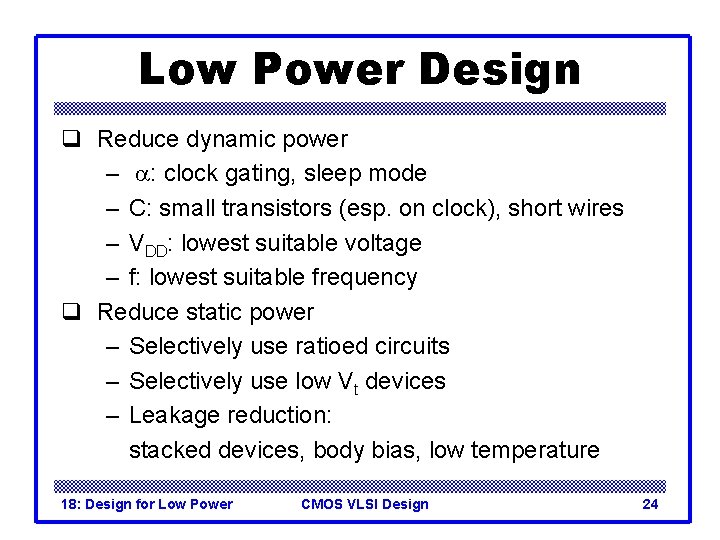
Low Power Design q Reduce dynamic power – a: clock gating, sleep mode – C: small transistors (esp. on clock), short wires – VDD: lowest suitable voltage – f: lowest suitable frequency q Reduce static power – Selectively use ratioed circuits – Selectively use low Vt devices – Leakage reduction: stacked devices, body bias, low temperature 18: Design for Low Power CMOS VLSI Design 24