Introduction to CMOS VLSI Design Lecture 10 Sequential


- Slides: 54

Introduction to CMOS VLSI Design Lecture 10: Sequential Circuits David Harris 10: Sequential Circuits Harvey Mudd College Spring 2004 1

Outline q q q q Floorplanning Sequencing Element Design Max and Min-Delay Clock Skew Time Borrowing Two-Phase Clocking 10: Sequential Circuits CMOS VLSI Design 2

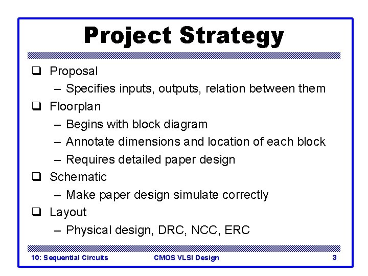
Project Strategy q Proposal – Specifies inputs, outputs, relation between them q Floorplan – Begins with block diagram – Annotate dimensions and location of each block – Requires detailed paper design q Schematic – Make paper design simulate correctly q Layout – Physical design, DRC, NCC, ERC 10: Sequential Circuits CMOS VLSI Design 3

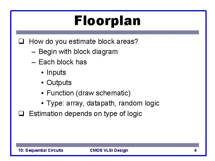
Floorplan q How do you estimate block areas? – Begin with block diagram – Each block has • Inputs • Outputs • Function (draw schematic) • Type: array, datapath, random logic q Estimation depends on type of logic 10: Sequential Circuits CMOS VLSI Design 4

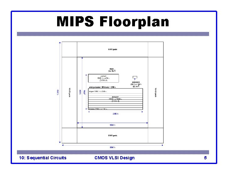
MIPS Floorplan 10: Sequential Circuits CMOS VLSI Design 5

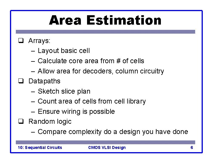
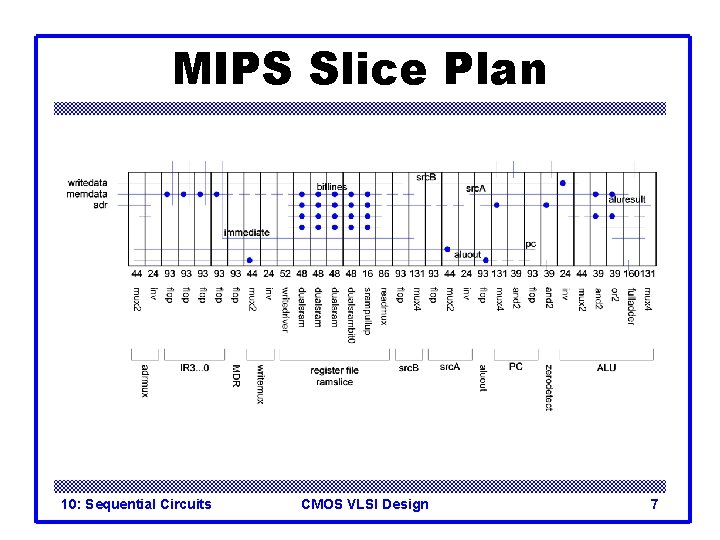
Area Estimation q Arrays: – Layout basic cell – Calculate core area from # of cells – Allow area for decoders, column circuitry q Datapaths – Sketch slice plan – Count area of cells from cell library – Ensure wiring is possible q Random logic – Compare complexity do a design you have done 10: Sequential Circuits CMOS VLSI Design 6

MIPS Slice Plan 10: Sequential Circuits CMOS VLSI Design 7

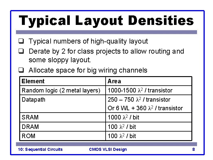
Typical Layout Densities q Typical numbers of high-quality layout q Derate by 2 for class projects to allow routing and some sloppy layout. q Allocate space for big wiring channels Element Area Random logic (2 metal layers) 1000 -1500 l 2 / transistor Datapath 250 – 750 l 2 / transistor Or 6 WL + 360 l 2 / transistor SRAM 1000 l 2 / bit DRAM 100 l 2 / bit ROM 100 l 2 / bit 10: Sequential Circuits CMOS VLSI Design 8

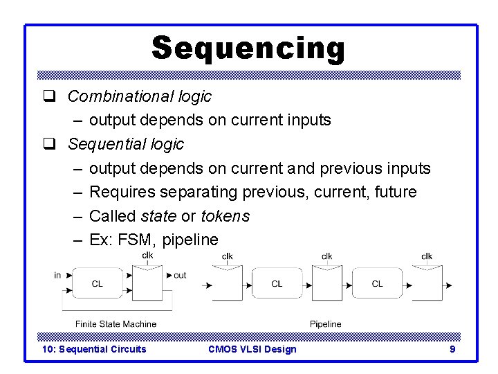
Sequencing q Combinational logic – output depends on current inputs q Sequential logic – output depends on current and previous inputs – Requires separating previous, current, future – Called state or tokens – Ex: FSM, pipeline 10: Sequential Circuits CMOS VLSI Design 9

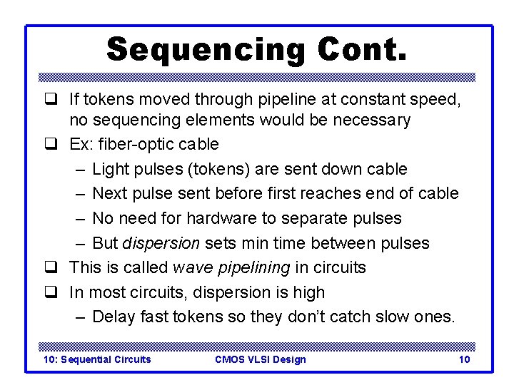
Sequencing Cont. q If tokens moved through pipeline at constant speed, no sequencing elements would be necessary q Ex: fiber-optic cable – Light pulses (tokens) are sent down cable – Next pulse sent before first reaches end of cable – No need for hardware to separate pulses – But dispersion sets min time between pulses q This is called wave pipelining in circuits q In most circuits, dispersion is high – Delay fast tokens so they don’t catch slow ones. 10: Sequential Circuits CMOS VLSI Design 10

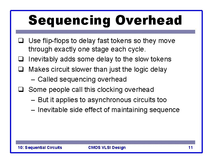
Sequencing Overhead q Use flip-flops to delay fast tokens so they move through exactly one stage each cycle. q Inevitably adds some delay to the slow tokens q Makes circuit slower than just the logic delay – Called sequencing overhead q Some people call this clocking overhead – But it applies to asynchronous circuits too – Inevitable side effect of maintaining sequence 10: Sequential Circuits CMOS VLSI Design 11

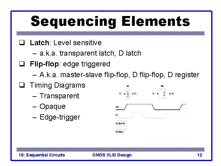
Sequencing Elements q Latch: Level sensitive – a. k. a. transparent latch, D latch q Flip-flop: edge triggered – A. k. a. master-slave flip-flop, D register q Timing Diagrams – Transparent – Opaque – Edge-trigger 10: Sequential Circuits CMOS VLSI Design 12

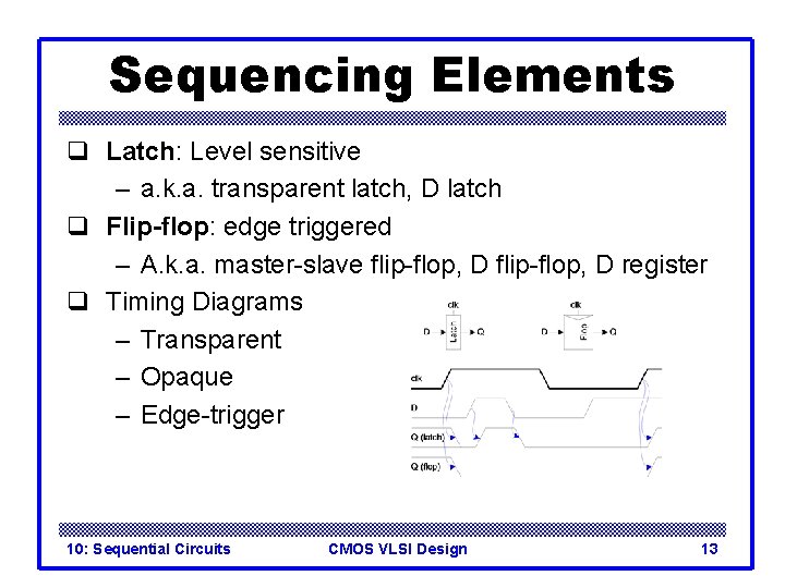
Sequencing Elements q Latch: Level sensitive – a. k. a. transparent latch, D latch q Flip-flop: edge triggered – A. k. a. master-slave flip-flop, D register q Timing Diagrams – Transparent – Opaque – Edge-trigger 10: Sequential Circuits CMOS VLSI Design 13

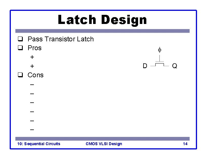
Latch Design q Pass Transistor Latch q Pros + + q Cons – – – 10: Sequential Circuits CMOS VLSI Design 14

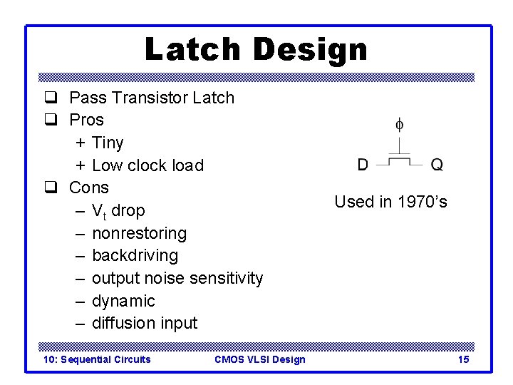
Latch Design q Pass Transistor Latch q Pros + Tiny + Low clock load q Cons – Vt drop – nonrestoring – backdriving – output noise sensitivity – dynamic – diffusion input 10: Sequential Circuits CMOS VLSI Design Used in 1970’s 15

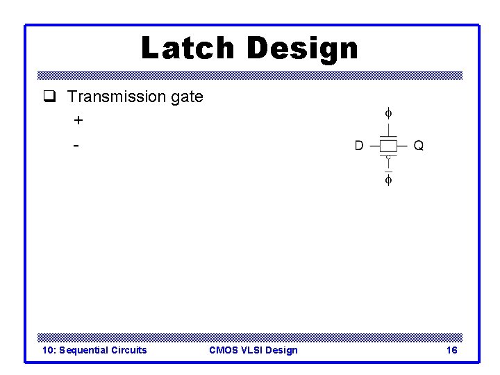
Latch Design q Transmission gate + - 10: Sequential Circuits CMOS VLSI Design 16

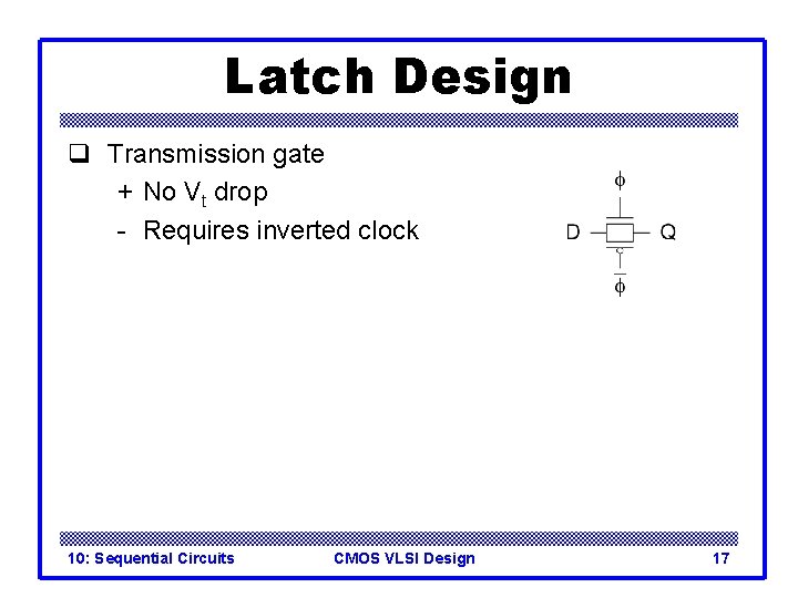
Latch Design q Transmission gate + No Vt drop - Requires inverted clock 10: Sequential Circuits CMOS VLSI Design 17

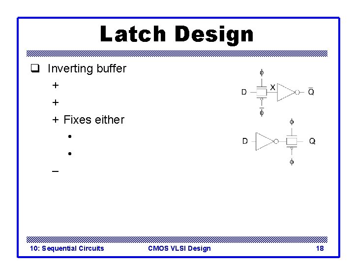
Latch Design q Inverting buffer + + + Fixes either • • – 10: Sequential Circuits CMOS VLSI Design 18

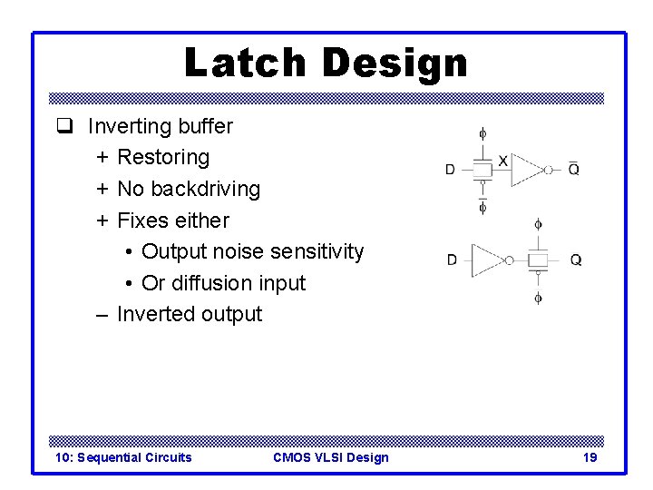
Latch Design q Inverting buffer + Restoring + No backdriving + Fixes either • Output noise sensitivity • Or diffusion input – Inverted output 10: Sequential Circuits CMOS VLSI Design 19

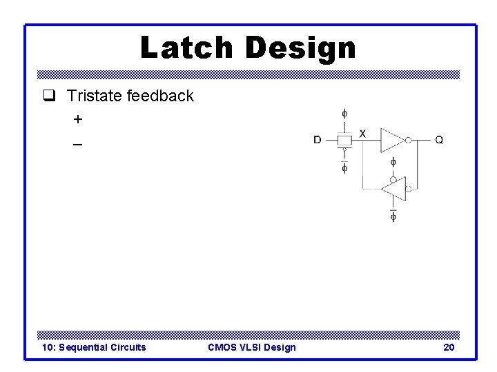
Latch Design q Tristate feedback + – 10: Sequential Circuits CMOS VLSI Design 20

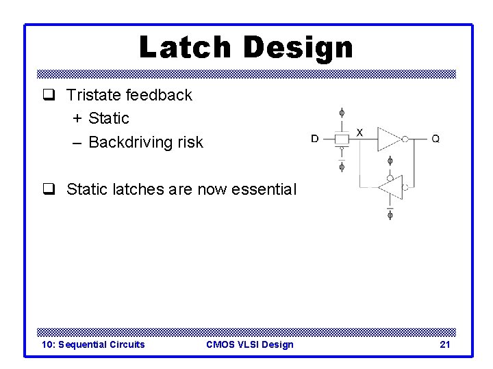
Latch Design q Tristate feedback + Static – Backdriving risk q Static latches are now essential 10: Sequential Circuits CMOS VLSI Design 21

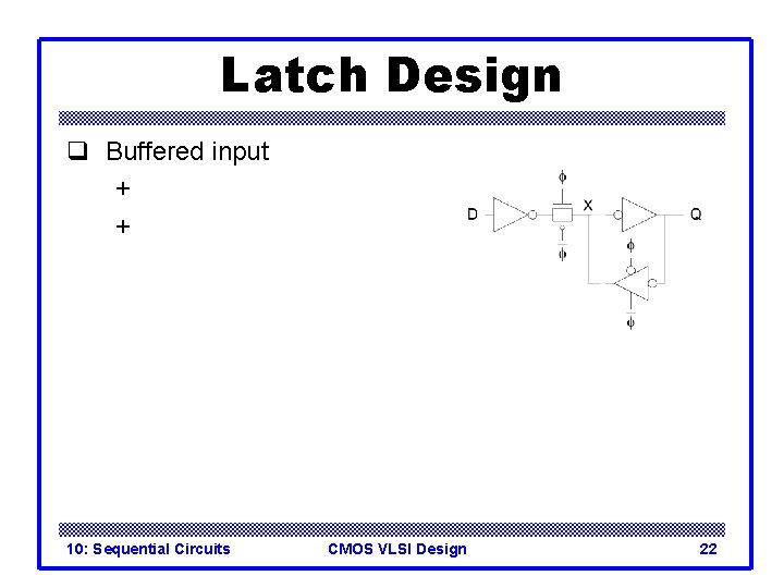
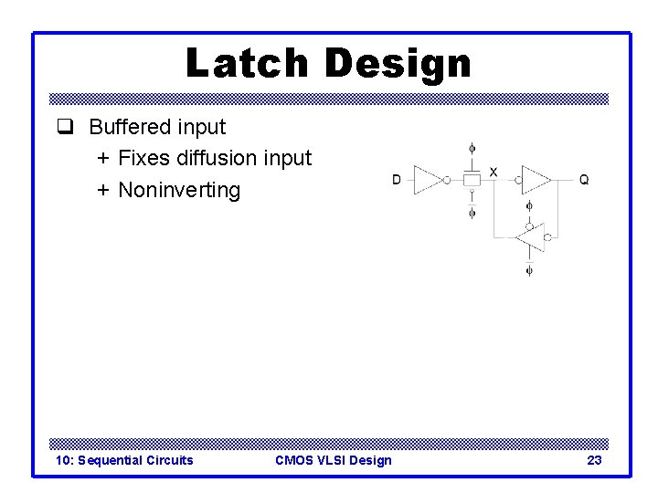
Latch Design q Buffered input + + 10: Sequential Circuits CMOS VLSI Design 22

Latch Design q Buffered input + Fixes diffusion input + Noninverting 10: Sequential Circuits CMOS VLSI Design 23

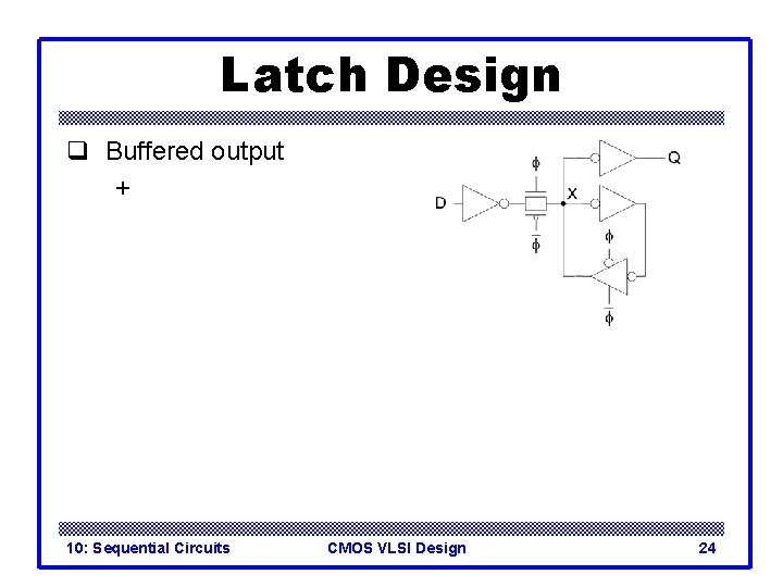
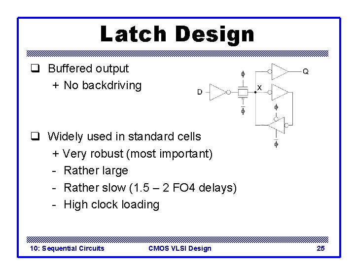
Latch Design q Buffered output + 10: Sequential Circuits CMOS VLSI Design 24

Latch Design q Buffered output + No backdriving q Widely used in standard cells + Very robust (most important) - Rather large - Rather slow (1. 5 – 2 FO 4 delays) - High clock loading 10: Sequential Circuits CMOS VLSI Design 25

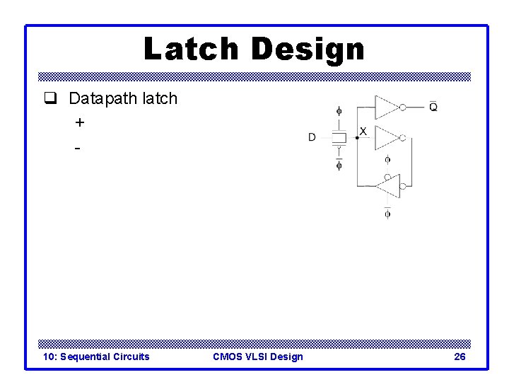
Latch Design q Datapath latch + - 10: Sequential Circuits CMOS VLSI Design 26

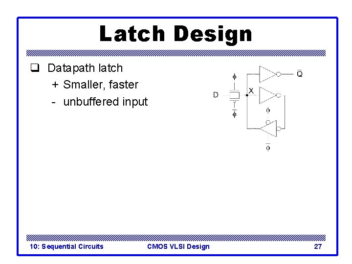
Latch Design q Datapath latch + Smaller, faster - unbuffered input 10: Sequential Circuits CMOS VLSI Design 27

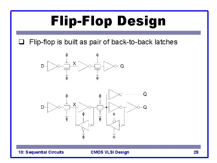
Flip-Flop Design q Flip-flop is built as pair of back-to-back latches 10: Sequential Circuits CMOS VLSI Design 28

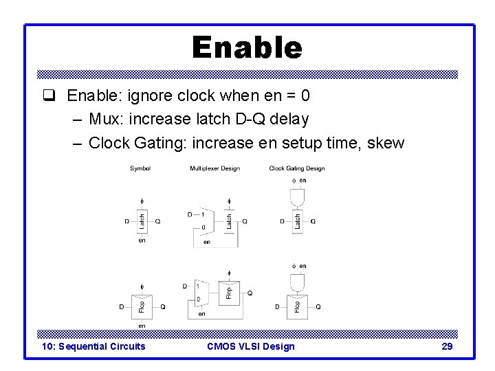
Enable q Enable: ignore clock when en = 0 – Mux: increase latch D-Q delay – Clock Gating: increase en setup time, skew 10: Sequential Circuits CMOS VLSI Design 29

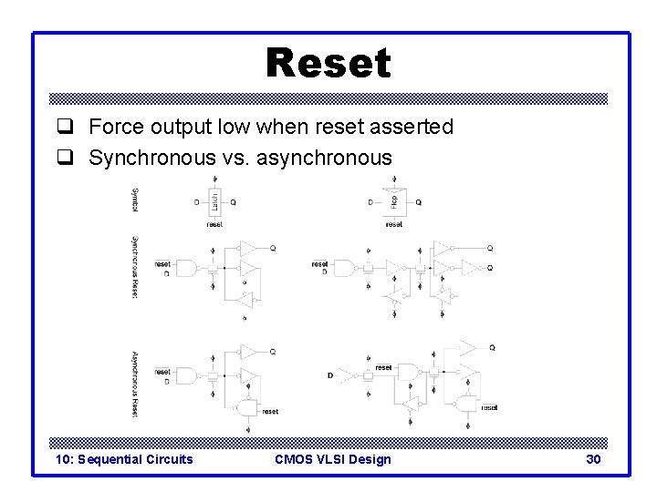
Reset q Force output low when reset asserted q Synchronous vs. asynchronous 10: Sequential Circuits CMOS VLSI Design 30

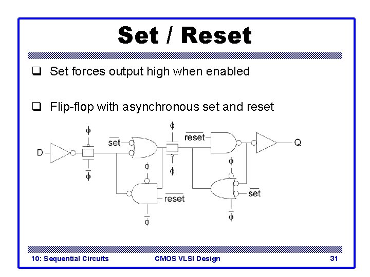
Set / Reset q Set forces output high when enabled q Flip-flop with asynchronous set and reset 10: Sequential Circuits CMOS VLSI Design 31

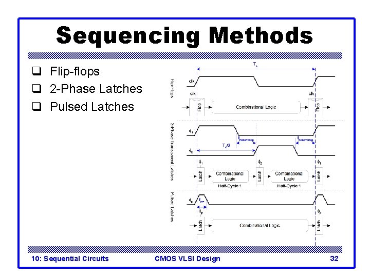
Sequencing Methods q Flip-flops q 2 -Phase Latches q Pulsed Latches 10: Sequential Circuits CMOS VLSI Design 32

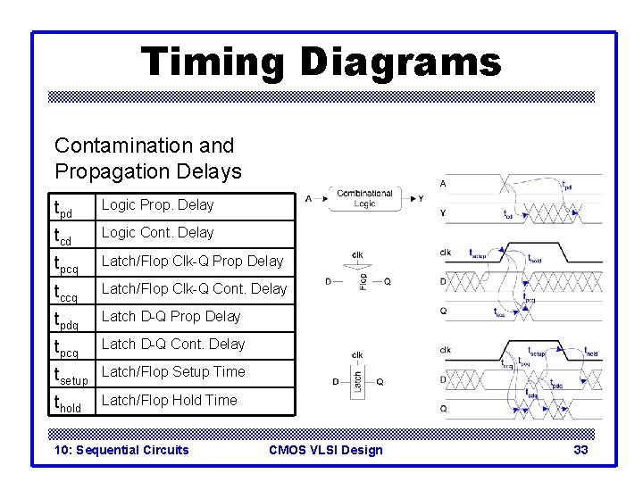
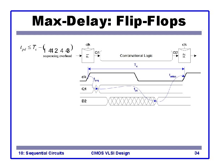
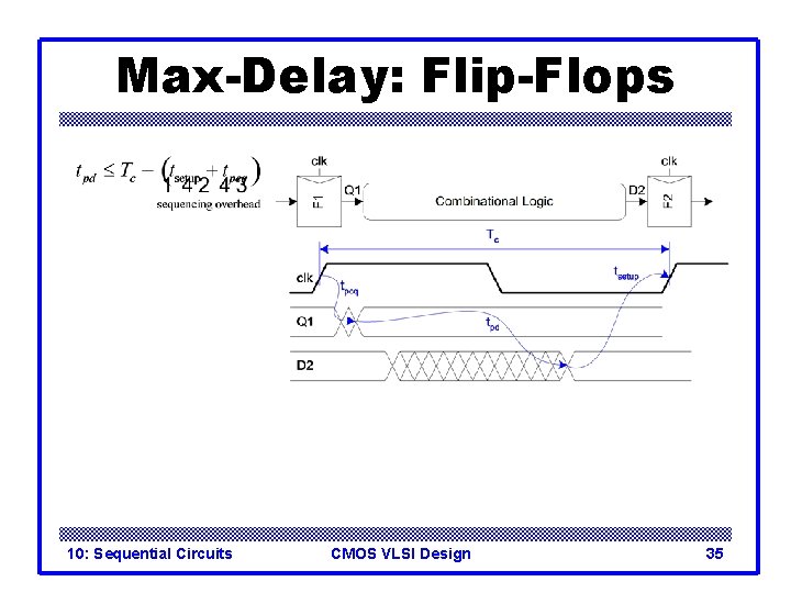
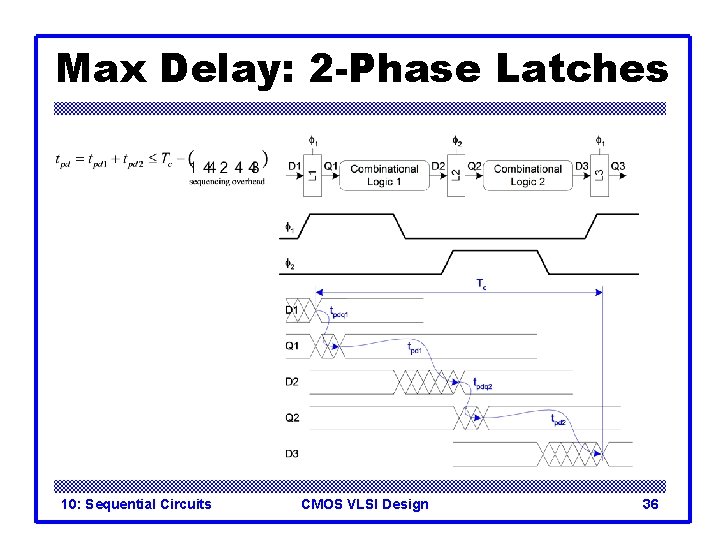
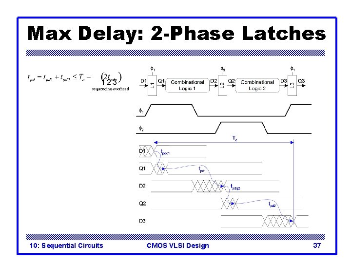
Timing Diagrams Contamination and Propagation Delays tpd Logic Prop. Delay tcd Logic Cont. Delay tpcq Latch/Flop Clk-Q Prop Delay tccq Latch/Flop Clk-Q Cont. Delay tpdq Latch D-Q Prop Delay tpcq Latch D-Q Cont. Delay tsetup Latch/Flop Setup Time thold Latch/Flop Hold Time 10: Sequential Circuits CMOS VLSI Design 33

Max-Delay: Flip-Flops 10: Sequential Circuits CMOS VLSI Design 34

Max-Delay: Flip-Flops 10: Sequential Circuits CMOS VLSI Design 35

Max Delay: 2 -Phase Latches 10: Sequential Circuits CMOS VLSI Design 36

Max Delay: 2 -Phase Latches 10: Sequential Circuits CMOS VLSI Design 37

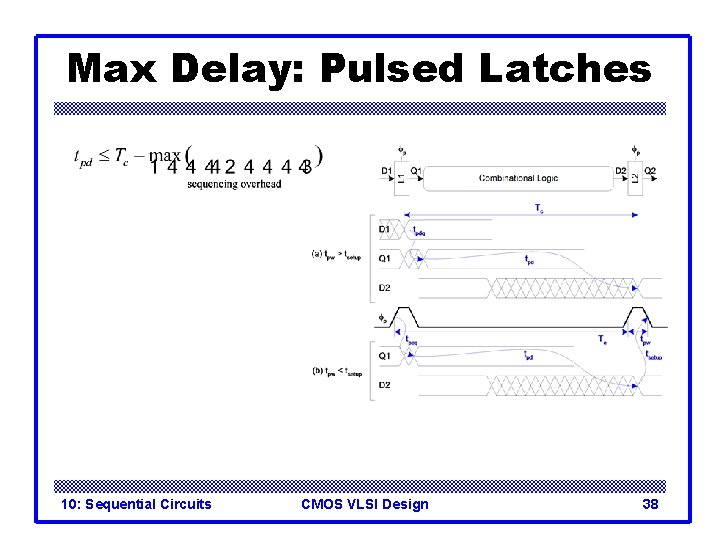
Max Delay: Pulsed Latches 10: Sequential Circuits CMOS VLSI Design 38

Max Delay: Pulsed Latches 10: Sequential Circuits CMOS VLSI Design 39

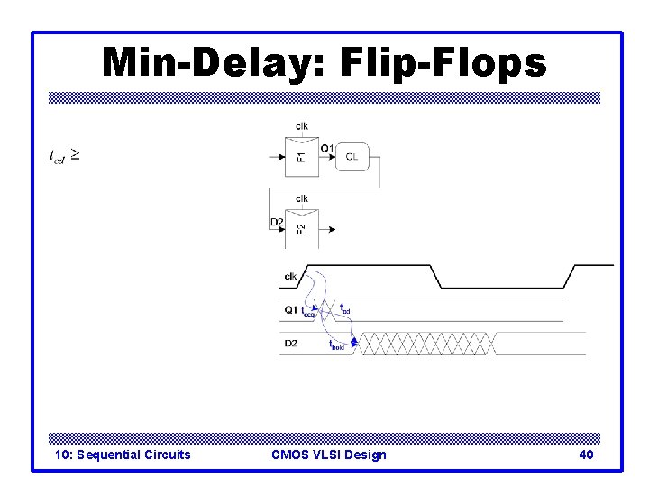
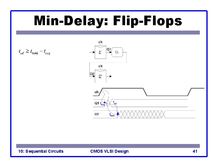
Min-Delay: Flip-Flops 10: Sequential Circuits CMOS VLSI Design 40

Min-Delay: Flip-Flops 10: Sequential Circuits CMOS VLSI Design 41

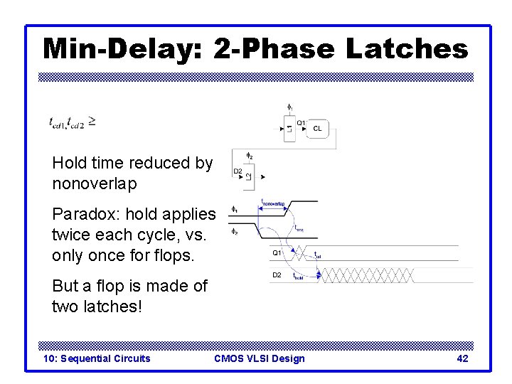
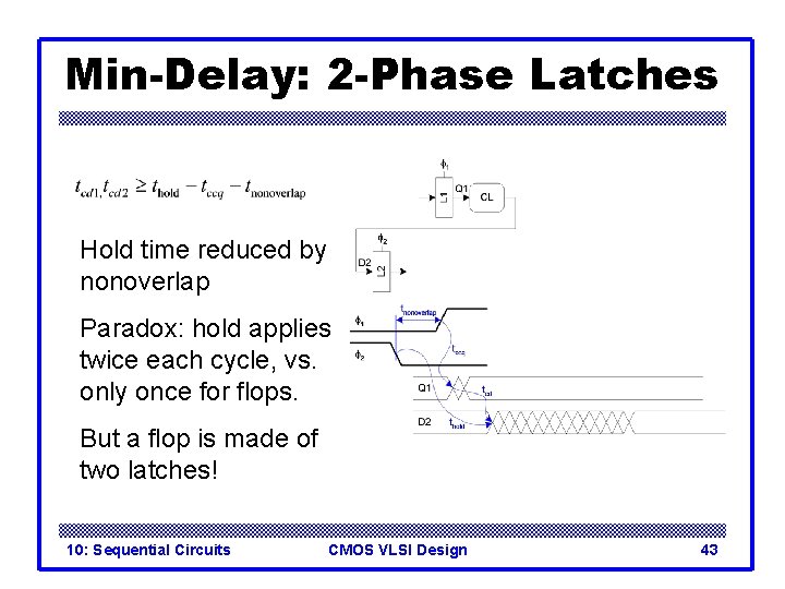
Min-Delay: 2 -Phase Latches Hold time reduced by nonoverlap Paradox: hold applies twice each cycle, vs. only once for flops. But a flop is made of two latches! 10: Sequential Circuits CMOS VLSI Design 42

Min-Delay: 2 -Phase Latches Hold time reduced by nonoverlap Paradox: hold applies twice each cycle, vs. only once for flops. But a flop is made of two latches! 10: Sequential Circuits CMOS VLSI Design 43

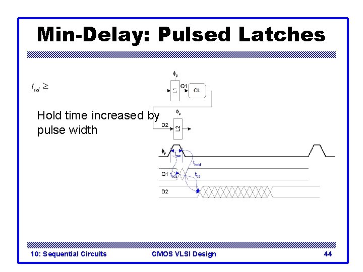
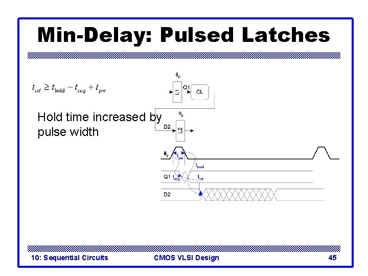
Min-Delay: Pulsed Latches Hold time increased by pulse width 10: Sequential Circuits CMOS VLSI Design 44

Min-Delay: Pulsed Latches Hold time increased by pulse width 10: Sequential Circuits CMOS VLSI Design 45

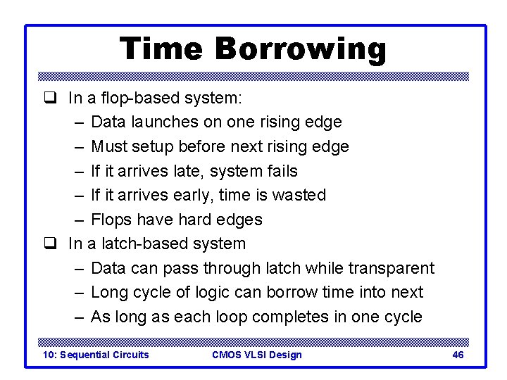
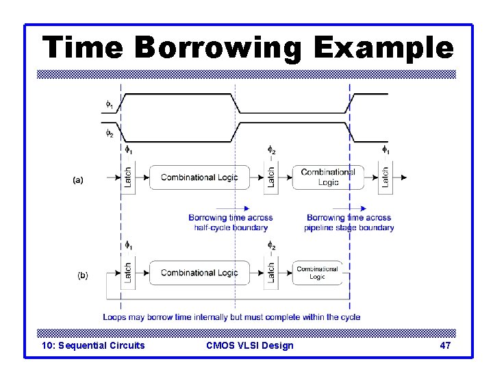
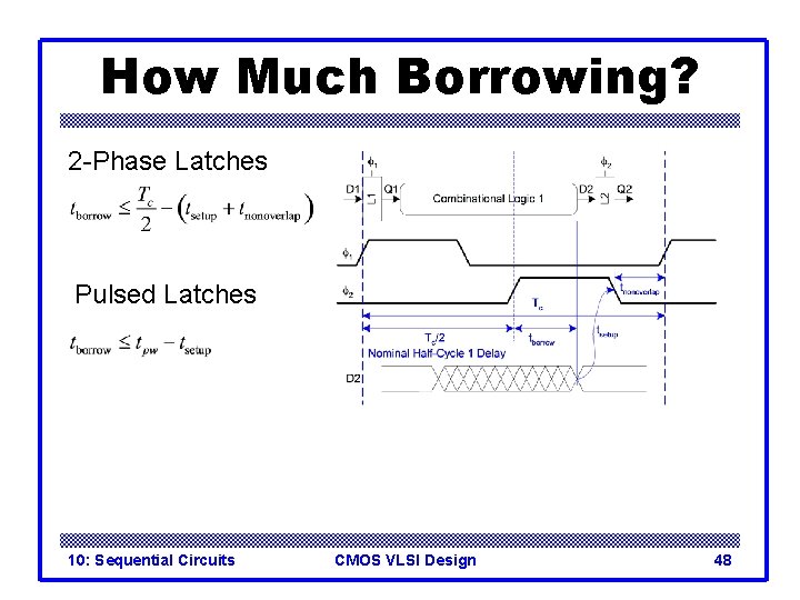
Time Borrowing q In a flop-based system: – Data launches on one rising edge – Must setup before next rising edge – If it arrives late, system fails – If it arrives early, time is wasted – Flops have hard edges q In a latch-based system – Data can pass through latch while transparent – Long cycle of logic can borrow time into next – As long as each loop completes in one cycle 10: Sequential Circuits CMOS VLSI Design 46

Time Borrowing Example 10: Sequential Circuits CMOS VLSI Design 47

How Much Borrowing? 2 -Phase Latches Pulsed Latches 10: Sequential Circuits CMOS VLSI Design 48

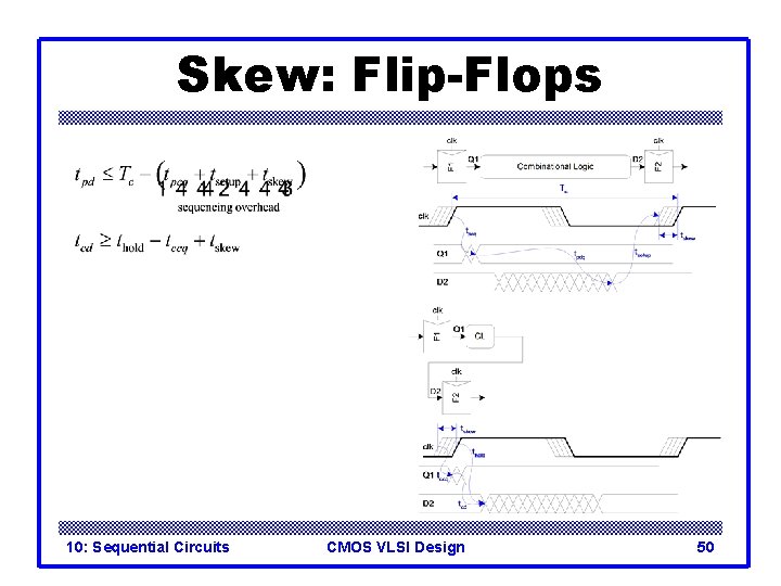
Clock Skew q We have assumed zero clock skew q Clocks really have uncertainty in arrival time – Decreases maximum propagation delay – Increases minimum contamination delay – Decreases time borrowing 10: Sequential Circuits CMOS VLSI Design 49

Skew: Flip-Flops 10: Sequential Circuits CMOS VLSI Design 50

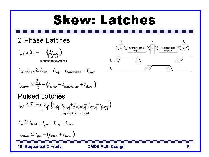
Skew: Latches 2 -Phase Latches Pulsed Latches 10: Sequential Circuits CMOS VLSI Design 51

Two-Phase Clocking q If setup times are violated, reduce clock speed q If hold times are violated, chip fails at any speed q In this class, working chips are most important – No tools to analyze clock skew q An easy way to guarantee hold times is to use 2 phase latches with big nonoverlap times q Call these clocks f 1, f 2 (ph 1, ph 2) 10: Sequential Circuits CMOS VLSI Design 52

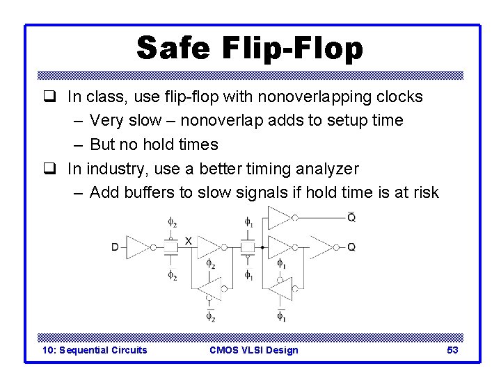
Safe Flip-Flop q In class, use flip-flop with nonoverlapping clocks – Very slow – nonoverlap adds to setup time – But no hold times q In industry, use a better timing analyzer – Add buffers to slow signals if hold time is at risk 10: Sequential Circuits CMOS VLSI Design 53

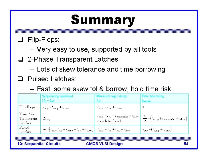
Summary q Flip-Flops: – Very easy to use, supported by all tools q 2 -Phase Transparent Latches: – Lots of skew tolerance and time borrowing q Pulsed Latches: – Fast, some skew tol & borrow, hold time risk 10: Sequential Circuits CMOS VLSI Design 54