Introduction to CMOS VLSI Design Lecture 0 Introduction

- Slides: 54

Introduction to CMOS VLSI Design Lecture 0: Introduction Credits: David Harris Harvey Mudd College (Material taken/adapted from Harris’ lecture notes) 0: Introduction 1

Outline q Course Information – Logistics – Grading – Syllabus – Course Overview q Introduction to VLSI – MOS transistors – CMOS logic gates – Fabrication process: overview 0: Introduction CMOS VLSI Design 2

Course Information (1) Time and Place – Tue/Thu 3: 30 -4: 45 pm, SN 325 Instructor – Montek Singh – montek@cs. unc. edu (not singh@cs!) – SN 245, 962 -1832 – Office hours: walk in most afternoons Course Web Page – http: //www. cs. unc. edu/~montek 0: Introduction CMOS VLSI Design 3

Course Information (2) Prerequisites – Computer organization (COMP 120), and digital logic (COMP 160, PHYS 102), or equivalent – I assume you know the following topics • Boolean algebra, logic gates, etc. • Undergraduate physics: Ohm’s law, resistors, capacitors, etc. • Undergraduate math: calculus 0: Introduction CMOS VLSI Design 4

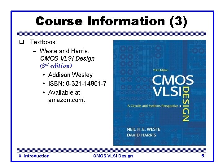
Course Information (3) q Textbook – Weste and Harris. CMOS VLSI Design (3 rd edition) • Addison Wesley • ISBN: 0 -321 -14901 -7 • Available at amazon. com. 0: Introduction CMOS VLSI Design 5

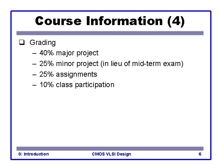
Course Information (4) q Grading – 40% major project – 25% minor project (in lieu of mid-term exam) – 25% assignments – 10% class participation 0: Introduction CMOS VLSI Design 6

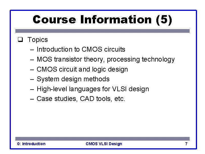
Course Information (5) q Topics – Introduction to CMOS circuits – MOS transistor theory, processing technology – CMOS circuit and logic design – System design methods – High-level languages for VLSI design – Case studies, CAD tools, etc. 0: Introduction CMOS VLSI Design 7

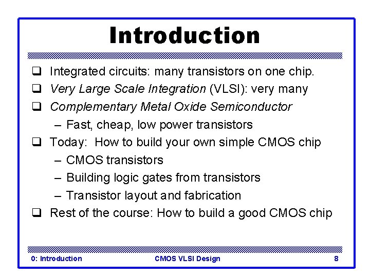
Introduction q Integrated circuits: many transistors on one chip. q Very Large Scale Integration (VLSI): very many q Complementary Metal Oxide Semiconductor – Fast, cheap, low power transistors q Today: How to build your own simple CMOS chip – CMOS transistors – Building logic gates from transistors – Transistor layout and fabrication q Rest of the course: How to build a good CMOS chip 0: Introduction CMOS VLSI Design 8

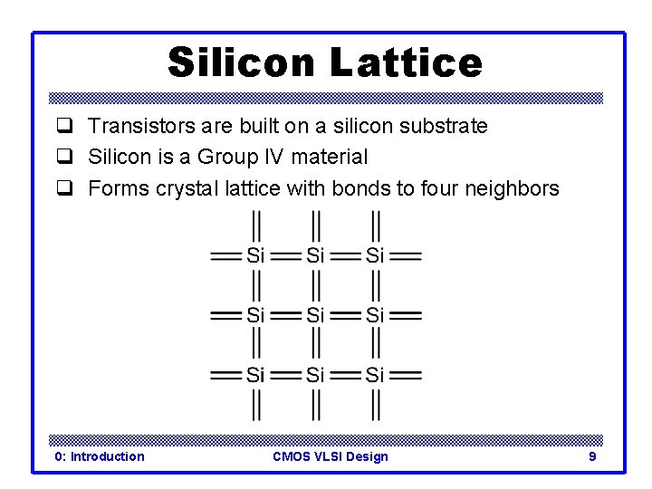
Silicon Lattice q Transistors are built on a silicon substrate q Silicon is a Group IV material q Forms crystal lattice with bonds to four neighbors 0: Introduction CMOS VLSI Design 9

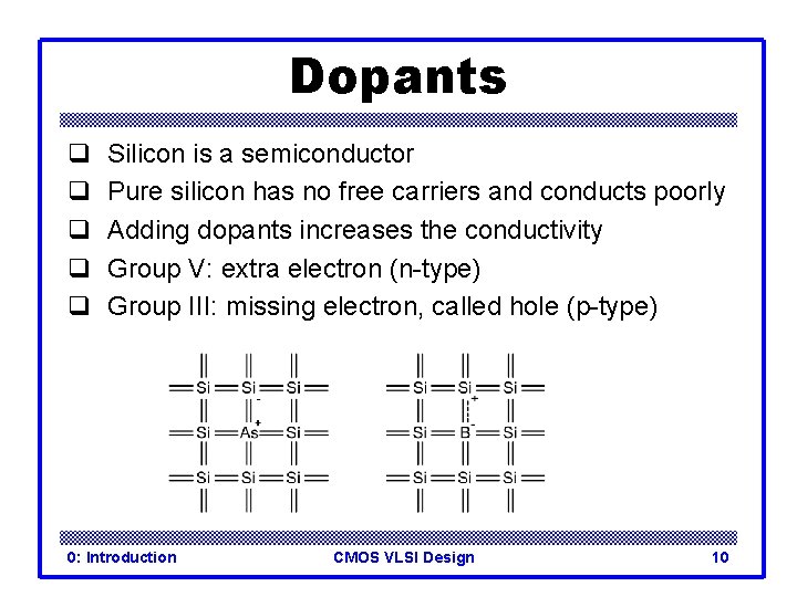
Dopants q q q Silicon is a semiconductor Pure silicon has no free carriers and conducts poorly Adding dopants increases the conductivity Group V: extra electron (n-type) Group III: missing electron, called hole (p-type) 0: Introduction CMOS VLSI Design 10

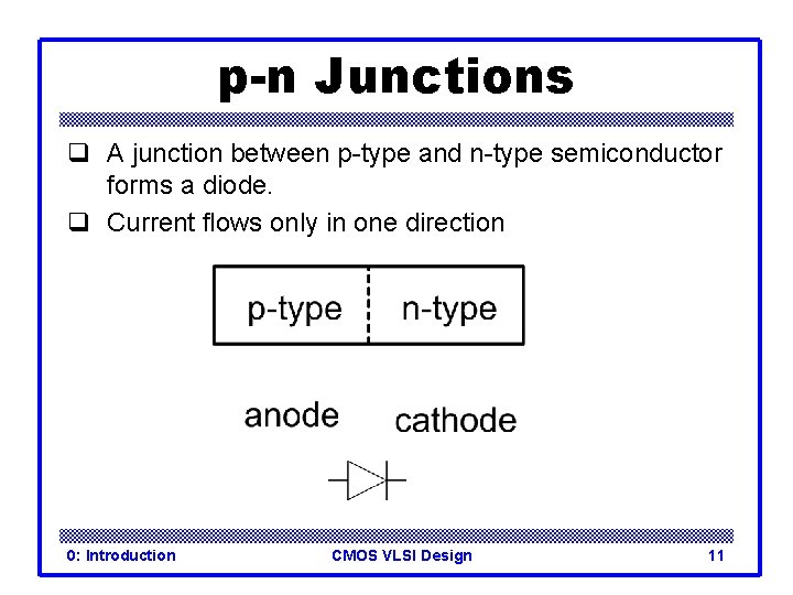
p-n Junctions q A junction between p-type and n-type semiconductor forms a diode. q Current flows only in one direction 0: Introduction CMOS VLSI Design 11

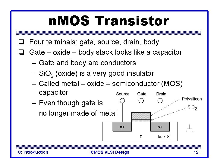
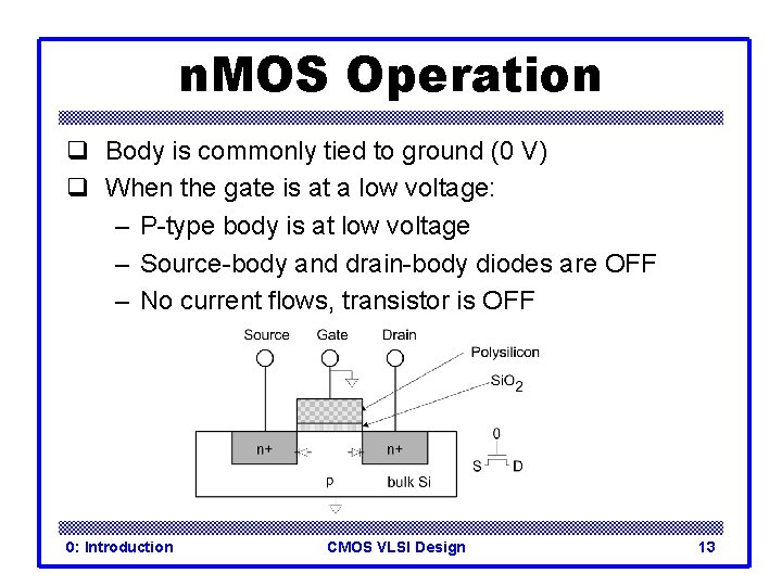
n. MOS Transistor q Four terminals: gate, source, drain, body q Gate – oxide – body stack looks like a capacitor – Gate and body are conductors – Si. O 2 (oxide) is a very good insulator – Called metal – oxide – semiconductor (MOS) capacitor – Even though gate is no longer made of metal 0: Introduction CMOS VLSI Design 12

n. MOS Operation q Body is commonly tied to ground (0 V) q When the gate is at a low voltage: – P-type body is at low voltage – Source-body and drain-body diodes are OFF – No current flows, transistor is OFF 0: Introduction CMOS VLSI Design 13

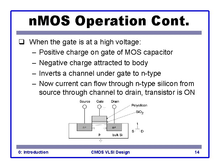
n. MOS Operation Cont. q When the gate is at a high voltage: – Positive charge on gate of MOS capacitor – Negative charge attracted to body – Inverts a channel under gate to n-type – Now current can flow through n-type silicon from source through channel to drain, transistor is ON 0: Introduction CMOS VLSI Design 14

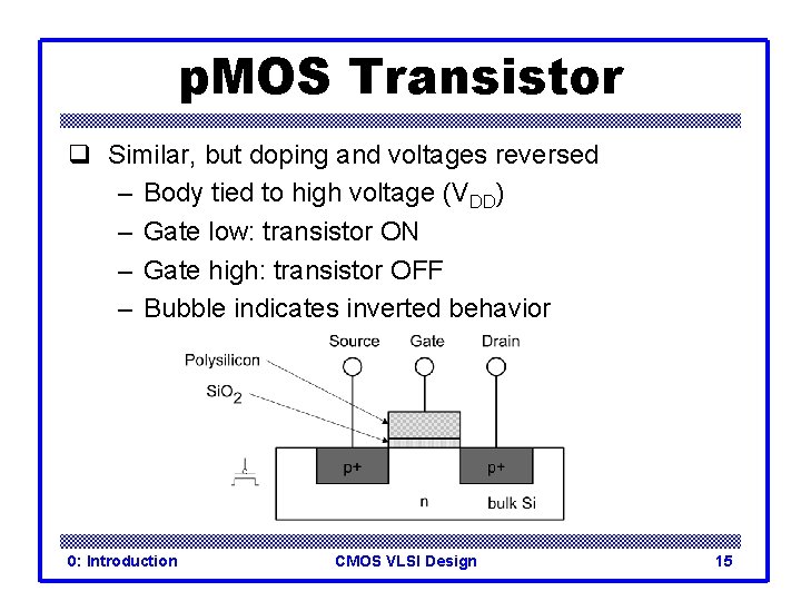
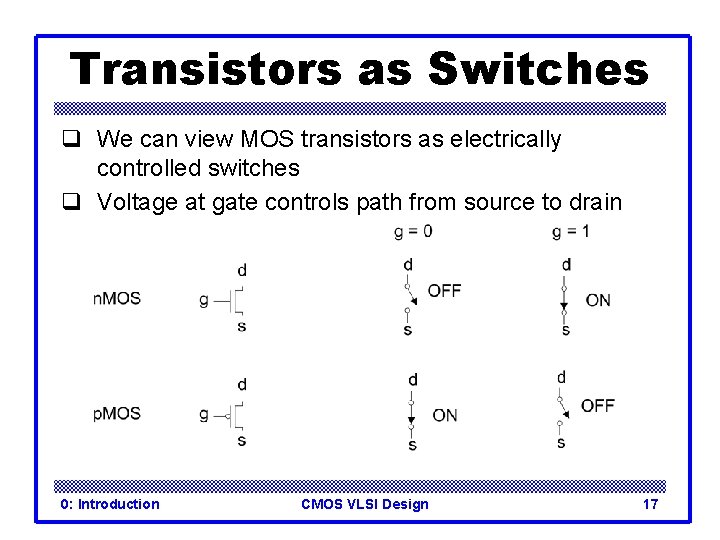
p. MOS Transistor q Similar, but doping and voltages reversed – Body tied to high voltage (VDD) – Gate low: transistor ON – Gate high: transistor OFF – Bubble indicates inverted behavior 0: Introduction CMOS VLSI Design 15

Power Supply Voltage q GND = 0 V q In 1980’s, VDD = 5 V q VDD has decreased in modern processes – High VDD would damage modern tiny transistors – Lower VDD saves power q VDD = 3. 3, 2. 5, 1. 8, 1. 5, 1. 2, 1. 0, … 0: Introduction CMOS VLSI Design 16

Transistors as Switches q We can view MOS transistors as electrically controlled switches q Voltage at gate controls path from source to drain 0: Introduction CMOS VLSI Design 17

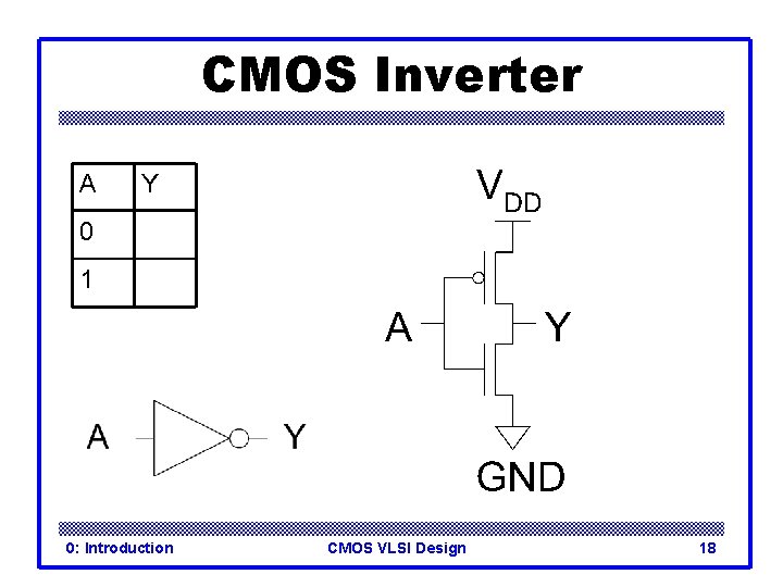
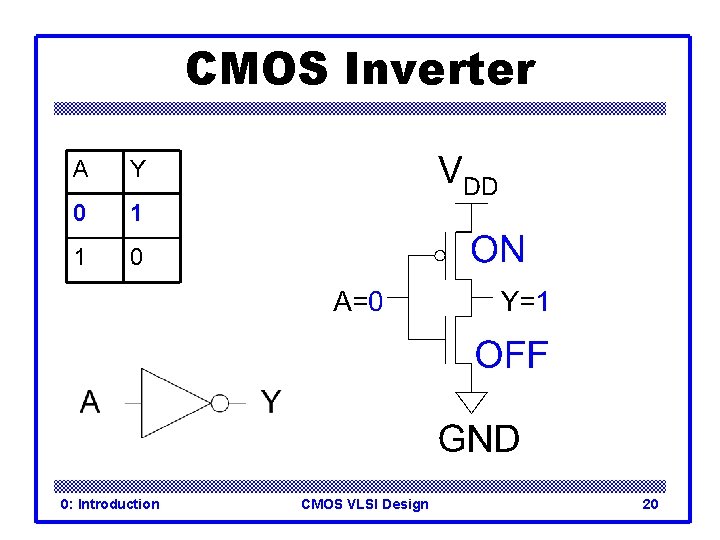
CMOS Inverter A Y 0 1 0: Introduction CMOS VLSI Design 18

CMOS Inverter A Y 0 1 0 0: Introduction CMOS VLSI Design 19

CMOS Inverter A Y 0 1 1 0 0: Introduction CMOS VLSI Design 20

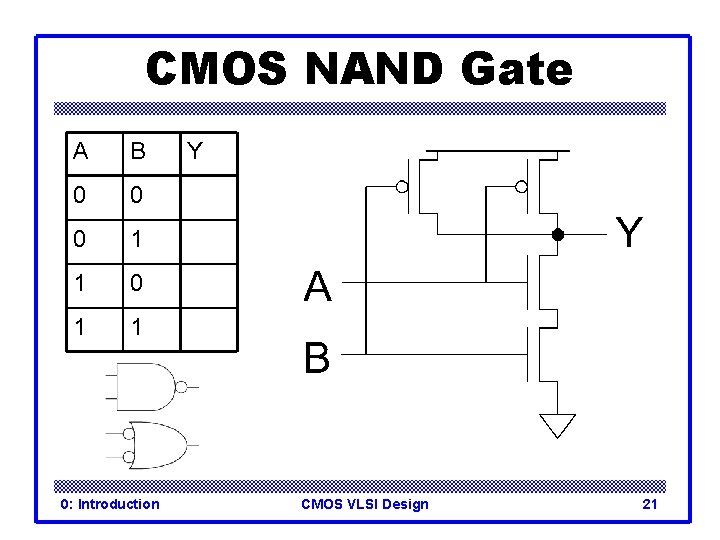
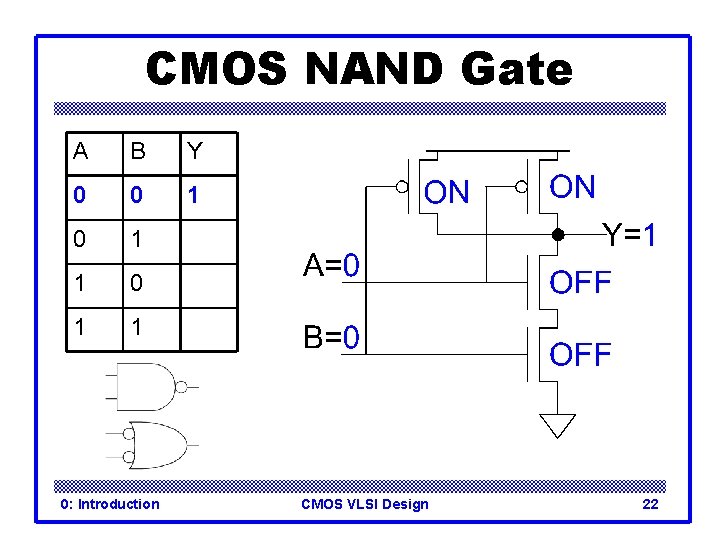
CMOS NAND Gate A B 0 0 0 1 1 0: Introduction Y CMOS VLSI Design 21

CMOS NAND Gate A B Y 0 0 1 1 0: Introduction CMOS VLSI Design 22

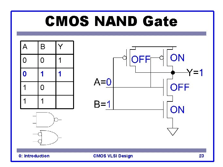
CMOS NAND Gate A B Y 0 0 1 1 1 0: Introduction CMOS VLSI Design 23

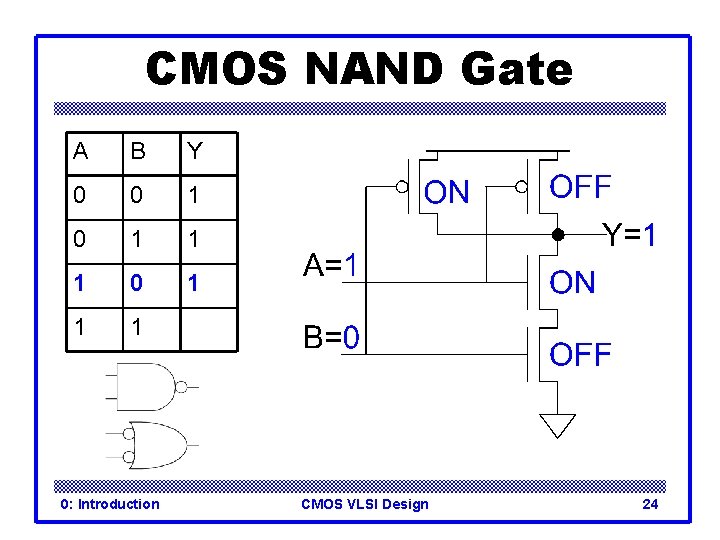
CMOS NAND Gate A B Y 0 0 1 1 1 0: Introduction CMOS VLSI Design 24

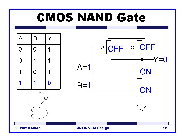
CMOS NAND Gate A B Y 0 0 1 1 1 0 0: Introduction CMOS VLSI Design 25

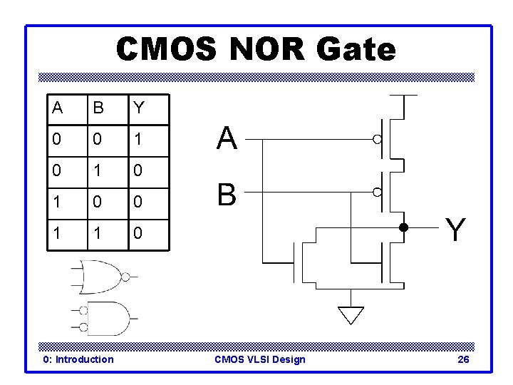
CMOS NOR Gate A B Y 0 0 1 0 1 0 0 1 1 0 0: Introduction CMOS VLSI Design 26

3 -input NAND Gate q Y pulls low if ALL inputs are 1 q Y pulls high if ANY input is 0 0: Introduction CMOS VLSI Design 27

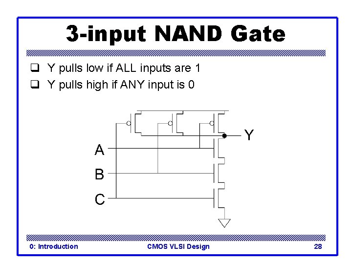
3 -input NAND Gate q Y pulls low if ALL inputs are 1 q Y pulls high if ANY input is 0 0: Introduction CMOS VLSI Design 28

CMOS Fabrication q CMOS transistors are fabricated on silicon wafer q Lithography process similar to printing press q On each step, different materials are deposited or etched q Easiest to understand by viewing both top and crosssection of wafer in a simplified manufacturing process 0: Introduction CMOS VLSI Design 29

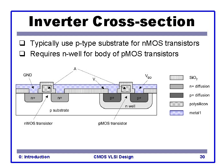
Inverter Cross-section q Typically use p-type substrate for n. MOS transistors q Requires n-well for body of p. MOS transistors 0: Introduction CMOS VLSI Design 30

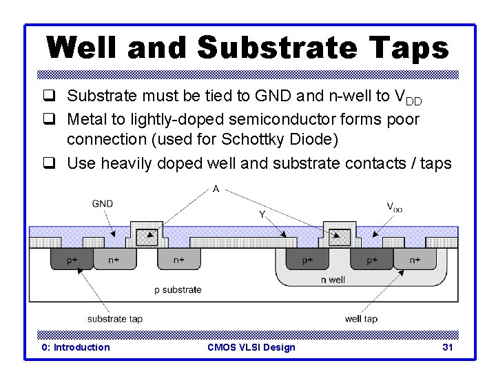
Well and Substrate Taps q Substrate must be tied to GND and n-well to VDD q Metal to lightly-doped semiconductor forms poor connection (used for Schottky Diode) q Use heavily doped well and substrate contacts / taps 0: Introduction CMOS VLSI Design 31

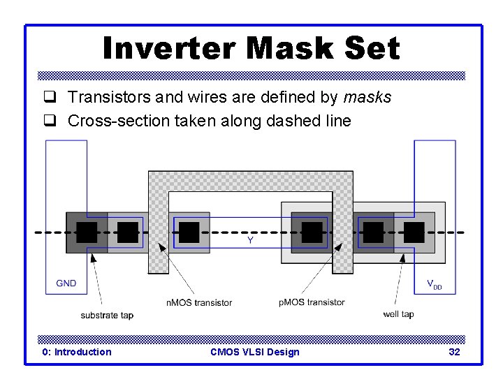
Inverter Mask Set q Transistors and wires are defined by masks q Cross-section taken along dashed line 0: Introduction CMOS VLSI Design 32

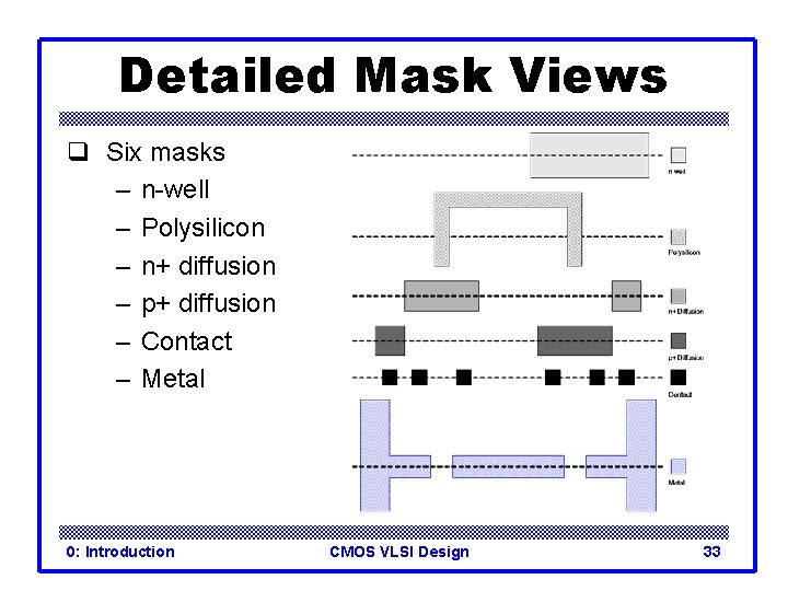
Detailed Mask Views q Six masks – n-well – Polysilicon – n+ diffusion – p+ diffusion – Contact – Metal 0: Introduction CMOS VLSI Design 33

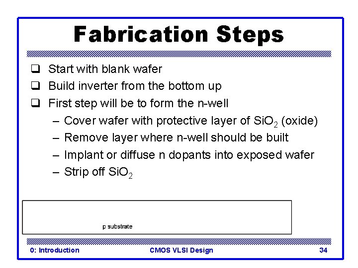
Fabrication Steps q Start with blank wafer q Build inverter from the bottom up q First step will be to form the n-well – Cover wafer with protective layer of Si. O 2 (oxide) – Remove layer where n-well should be built – Implant or diffuse n dopants into exposed wafer – Strip off Si. O 2 0: Introduction CMOS VLSI Design 34

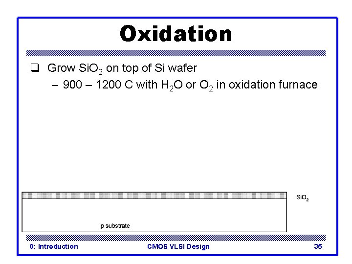
Oxidation q Grow Si. O 2 on top of Si wafer – 900 – 1200 C with H 2 O or O 2 in oxidation furnace 0: Introduction CMOS VLSI Design 35

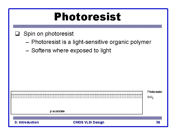
Photoresist q Spin on photoresist – Photoresist is a light-sensitive organic polymer – Softens where exposed to light 0: Introduction CMOS VLSI Design 36

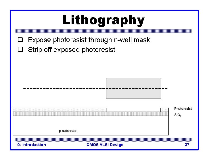
Lithography q Expose photoresist through n-well mask q Strip off exposed photoresist 0: Introduction CMOS VLSI Design 37

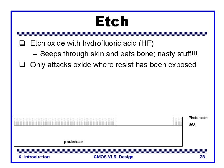
Etch q Etch oxide with hydrofluoric acid (HF) – Seeps through skin and eats bone; nasty stuff!!! q Only attacks oxide where resist has been exposed 0: Introduction CMOS VLSI Design 38

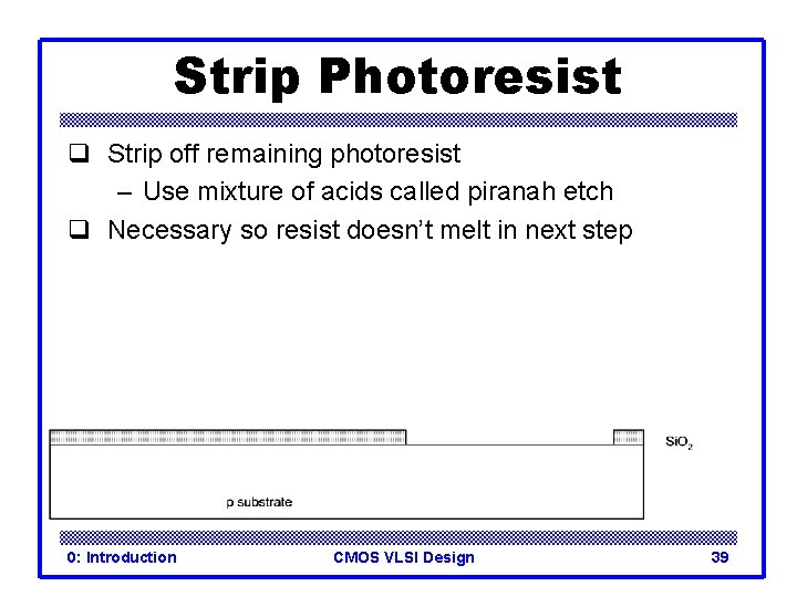
Strip Photoresist q Strip off remaining photoresist – Use mixture of acids called piranah etch q Necessary so resist doesn’t melt in next step 0: Introduction CMOS VLSI Design 39

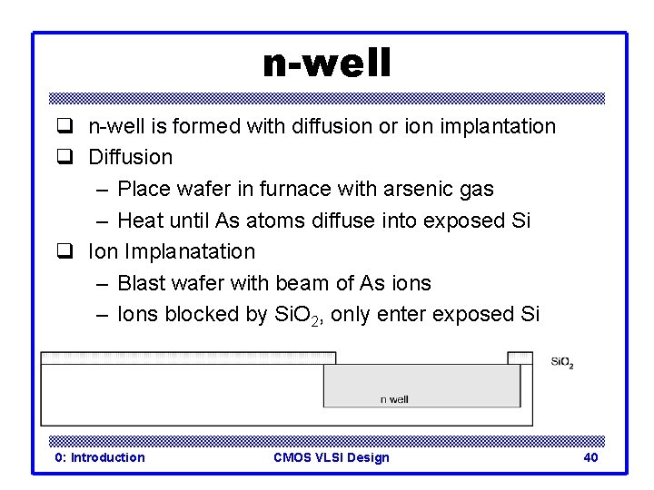
n-well q n-well is formed with diffusion or ion implantation q Diffusion – Place wafer in furnace with arsenic gas – Heat until As atoms diffuse into exposed Si q Ion Implanatation – Blast wafer with beam of As ions – Ions blocked by Si. O 2, only enter exposed Si 0: Introduction CMOS VLSI Design 40

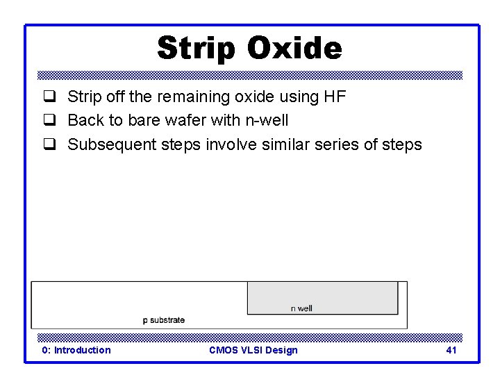
Strip Oxide q Strip off the remaining oxide using HF q Back to bare wafer with n-well q Subsequent steps involve similar series of steps 0: Introduction CMOS VLSI Design 41

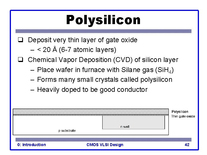
Polysilicon q Deposit very thin layer of gate oxide – < 20 Å (6 -7 atomic layers) q Chemical Vapor Deposition (CVD) of silicon layer – Place wafer in furnace with Silane gas (Si. H 4) – Forms many small crystals called polysilicon – Heavily doped to be good conductor 0: Introduction CMOS VLSI Design 42

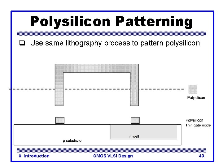
Polysilicon Patterning q Use same lithography process to pattern polysilicon 0: Introduction CMOS VLSI Design 43

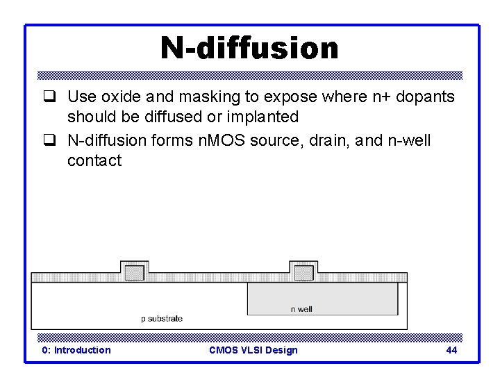
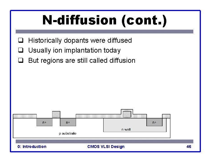
N-diffusion q Use oxide and masking to expose where n+ dopants should be diffused or implanted q N-diffusion forms n. MOS source, drain, and n-well contact 0: Introduction CMOS VLSI Design 44

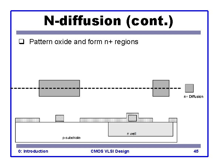
N-diffusion (cont. ) q Pattern oxide and form n+ regions 0: Introduction CMOS VLSI Design 45

N-diffusion (cont. ) q Historically dopants were diffused q Usually ion implantation today q But regions are still called diffusion 0: Introduction CMOS VLSI Design 46

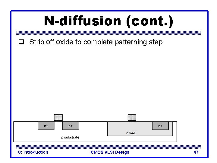
N-diffusion (cont. ) q Strip off oxide to complete patterning step 0: Introduction CMOS VLSI Design 47

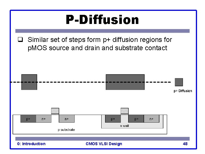
P-Diffusion q Similar set of steps form p+ diffusion regions for p. MOS source and drain and substrate contact 0: Introduction CMOS VLSI Design 48

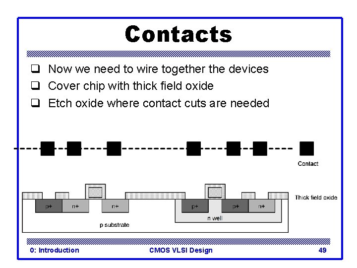
Contacts q Now we need to wire together the devices q Cover chip with thick field oxide q Etch oxide where contact cuts are needed 0: Introduction CMOS VLSI Design 49

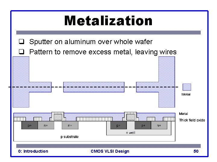
Metalization q Sputter on aluminum over whole wafer q Pattern to remove excess metal, leaving wires 0: Introduction CMOS VLSI Design 50

Layout q Chips are specified with set of masks q Minimum dimensions of masks determine transistor size (and hence speed, cost, and power) q Feature size f = distance between source and drain – Set by minimum width of polysilicon q Feature size improves 30% every 3 years or so q Normalize for feature size when describing design rules q Express rules in terms of l = f/2 – E. g. l = 0. 3 mm in 0. 6 mm process 0: Introduction CMOS VLSI Design 51

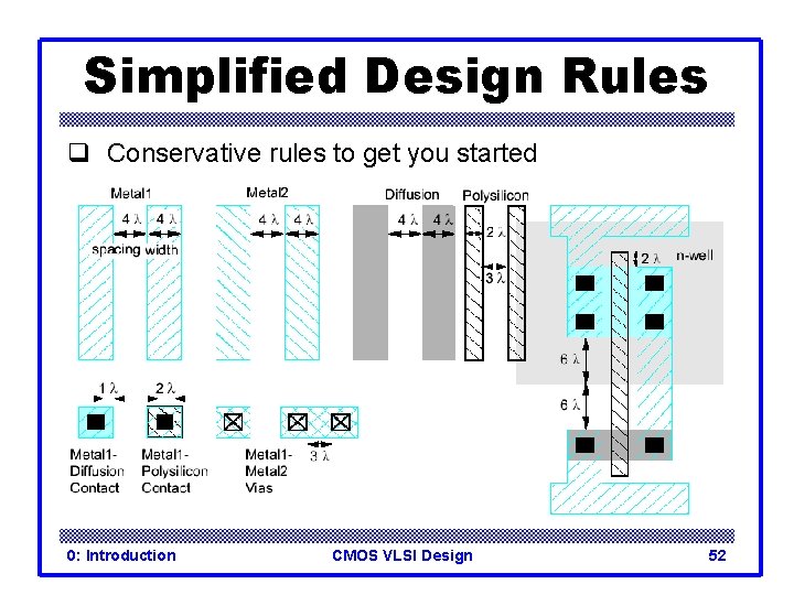
Simplified Design Rules q Conservative rules to get you started 0: Introduction CMOS VLSI Design 52

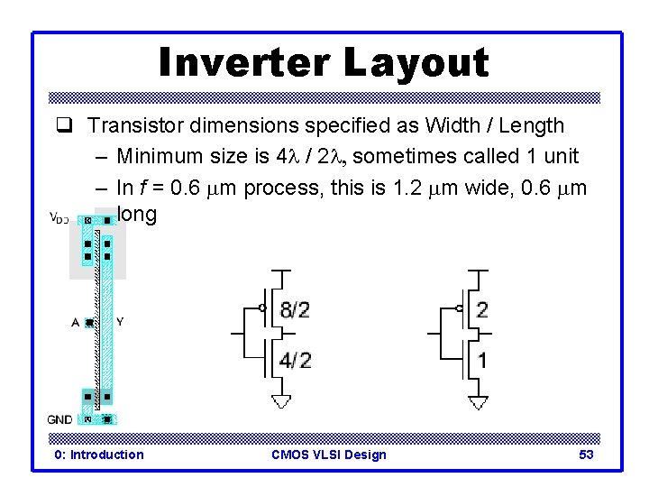
Inverter Layout q Transistor dimensions specified as Width / Length – Minimum size is 4 l / 2 l, sometimes called 1 unit – In f = 0. 6 mm process, this is 1. 2 mm wide, 0. 6 mm long 0: Introduction CMOS VLSI Design 53

Summary q q MOS Transistors are stack of gate, oxide, silicon Can be viewed as electrically controlled switches Build logic gates out of switches Draw masks to specify layout of transistors q Now you know everything necessary to start designing schematics and layout for a simple chip! 0: Introduction CMOS VLSI Design 54