INTRODUCTION TO BASIC POWER SUPPLIES POWER SUPPLY SYSTEM

INTRODUCTION TO BASIC POWER SUPPLIES
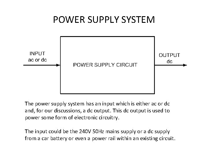
POWER SUPPLY SYSTEM The power supply system has an input which is either ac or dc and, for our discussions, a dc output. This dc output is used to power some form of electronic circuitry. The input could be the 240 V 50 Hz mains supply or a dc supply from a car battery or even a power rail within an existing circuit.
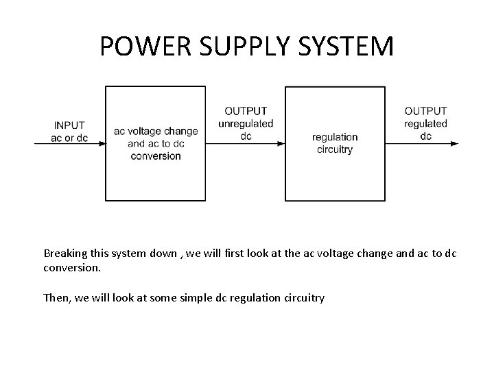
POWER SUPPLY SYSTEM Breaking this system down , we will first look at the ac voltage change and ac to dc conversion. Then, we will look at some simple dc regulation circuitry
Mains input aspects Usually, the ac input is 240 V rms, 50 Hz mains supply. CAUTION this voltage is LETHAL Take extra care when handling mains powered equipment, make sure of your safety when constructing and testing. PLUS make sure that adequate insulation and construction techniques are employed in the unit.
Mains input aspects Mains powered equipment must be properly protected by a fuse and double power switch. The mains powered equipment container (box) must be earthed if metallic or double insulation techniques employed to provide input to output isolation. A lot of consumer electronic units (TV, DVD players and the like) utilise double insulation techniques, so their mains input power lead only contains Live and Neutral wires, rather than also including an earth wire as well. Double insulation techniques present at least two ‘high voltage’ insulation barriers between the mains input circuitry and the system being powered. For example, the mains transformer has its primary (high voltage) winding on one bobbin and its secondary winding an a separate bobbin. Thus, if the primary winding burns up, the mains voltage cannot reach the ‘secondary side’. If in any doubt, connect the box to mains earth.
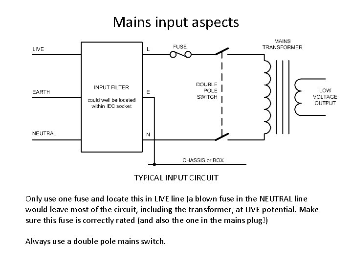
Mains input aspects TYPICAL INPUT CIRCUIT Only use one fuse and locate this in LIVE line (a blown fuse in the NEUTRAL line would leave most of the circuit, including the transformer, at LIVE potential. Make sure this fuse is correctly rated (and also the one in the mains plug!) Always use a double pole mains switch.
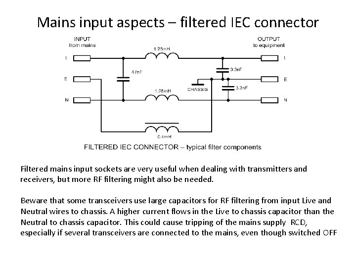
Mains input aspects – filtered IEC connector Filtered mains input sockets are very useful when dealing with transmitters and receivers, but more RF filtering might also be needed. Beware that some transceivers use large capacitors for RF filtering from input Live and Neutral wires to chassis. A higher current flows in the Live to chassis capacitor than the Neutral to chassis capacitor. This could cause tripping of the mains supply RCD, especially if several transceivers are connected to the mains, even though switched OFF
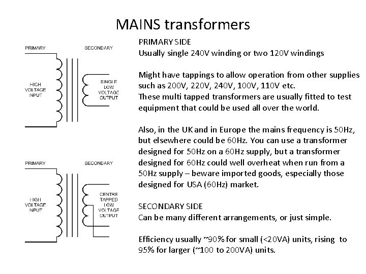
MAINS transformers PRIMARY SIDE Usually single 240 V winding or two 120 V windings Might have tappings to allow operation from other supplies such as 200 V, 220 V, 240 V, 100 V, 110 V etc. These multi tapped transformers are usually fitted to test equipment that could be used all over the world. Also, in the UK and in Europe the mains frequency is 50 Hz, but elsewhere could be 60 Hz. You can use a transformer designed for 50 Hz on a 60 Hz supply, but a transformer designed for 60 Hz could well overheat when run from a 50 Hz supply – beware imported goods, especially those designed for USA (60 Hz) market. SECONDARY SIDE Can be many different arrangements, or just simple. Efficiency usually ~90% for small (<20 VA) units, rising to 95% for larger (~100 to 200 VA) units.
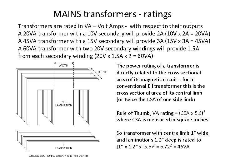
MAINS transformers - ratings Transformers are rated in VA – Volt Amps - with respect to their outputs A 20 VA transformer with a 10 V secondary will provide 2 A (10 V x 2 A = 20 VA) A 45 VA transformer with a 15 V secondary will provide 3 A (15 V x 3 A = 45 VA) A 60 VA transformer with two 20 V secondary windings will provide 1. 5 A from each secondary winding (20 V x 1. 5 A x 2 = 60 VA) The power rating of a transformer is directly related to the cross sectional area of its magnetic circuit – for a conventional E I transformer this is the cross sectional area of its central limb (or twice the CSA of one side limb) Rule of Thumb, VA rating = (CSA x 5. 6)2 where CSA is measured in square inches So transformer with centre limb 1” wide and laminations 1. 2” deep is rated to (1” x 1. 2” x 5. 6)2 = 6. 722 = 45 VA
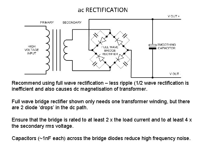
ac RECTIFICATION Recommend using full wave rectification – less ripple (1/2 wave rectification is inefficient and also causes dc magnetisation of transformer. Full wave bridge rectifier shown only needs one transformer winding, but there are 2 diode ‘drops’ in the dc path. Ensure that the bridge is rated to at least 2 x the load current and to at least 4 x the secondary rms voltage. Capacitors (~1 n. F each) across the bridge diodes reduce high frequency noise.
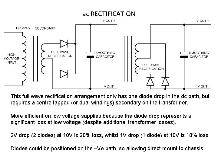
ac RECTIFICATION This full wave rectification arrangement only has one diode drop in the dc path, but requires a centre tapped (or dual windings) secondary on the transformer. More efficient on low voltage supplies because the diode drop represents a significant loss at low voltage (despite additional transformer losses). 2 V drop (2 diodes) at 10 V is 20% loss, whilst 1 V drop (1 diode) at 10 V is 10% loss Diodes could be positioned on the –Ve path, so allowing direct mount to chassis.
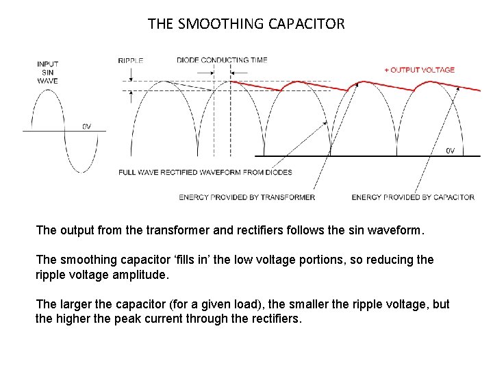
THE SMOOTHING CAPACITOR The output from the transformer and rectifiers follows the sin waveform. The smoothing capacitor ‘fills in’ the low voltage portions, so reducing the ripple voltage amplitude. The larger the capacitor (for a given load), the smaller the ripple voltage, but the higher the peak current through the rectifiers.
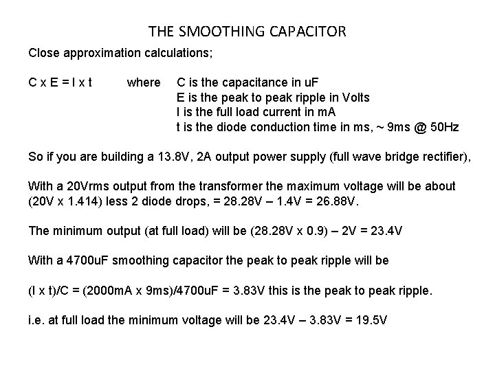
THE SMOOTHING CAPACITOR Close approximation calculations; Cx. E=Ixt where C is the capacitance in u. F E is the peak to peak ripple in Volts I is the full load current in m. A t is the diode conduction time in ms, ~ 9 ms @ 50 Hz So if you are building a 13. 8 V, 2 A output power supply (full wave bridge rectifier), With a 20 Vrms output from the transformer the maximum voltage will be about (20 V x 1. 414) less 2 diode drops, = 28. 28 V – 1. 4 V = 26. 88 V. The minimum output (at full load) will be (28. 28 V x 0. 9) – 2 V = 23. 4 V With a 4700 u. F smoothing capacitor the peak to peak ripple will be (I x t)/C = (2000 m. A x 9 ms)/4700 u. F = 3. 83 V this is the peak to peak ripple. i. e. at full load the minimum voltage will be 23. 4 V – 3. 83 V = 19. 5 V
THE SMOOTHING CAPACITOR Taking our example, The maximum voltage on the capacitor will be the no load value of 26. 88 V, so the capacitor needs to be rated for >>27 V, say at least 35 V or (better) 40 V. With a PSU output voltage of 13. 8 V and a full load minimum voltage of 19. 5 V, the PSU regulator has to be able to work with a minimum ‘headroom’ (difference between input and output) of 19. 5 V – 13. 8 V = 5. 7 V. You can now work out the maximum power dissipation in the PSU output stage. At full load, maximum dc level is 23. 4 V and the PSU output is 13. 8 V at 2 A So dissipation is (23. 4 V – 13. 8 V) x 2 A = 19. 2 W use a largish heatsink! 3. 83 V peak to peak ripple on a 23. 4 V supply represents just over 16%. Rule of thumb, with about 20 V transformer output, full wave rectified 50 Hz, using a capacitance of 2000 u. F per Amp loading will give you about 20% ripple.
DC POWER SUPPLY CIRCUITS Now we have converted our mains supply to a dc supply, albeit with some ripple, we can look at regulating dc supplies. This section also applies where we already have dc input supplies, for example from a car battery or from a ‘wall wart’ power supply that was used for something else, or even if we want to add some extra circuitry to an existing unit. We will start with basic, low power, circuitry and then increase the power, whilst trying to keep the technicalities to a minimum. Switched mode circuits are not discussed here because, generally, they are beyond the capabilities of home constructors, needing specially wound magnetic components and quite complex circuitry.
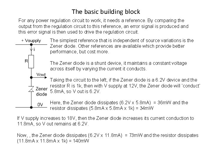
The basic building block For any power regulation circuit to work, it needs a reference. By comparing the output from the regulation circuit to this reference, an error signal is produced and this error signal is then used to drive the regulation circuit. The simplest reference that is independent of source variations is the Zener diode. Other references are available which provide better performance, but cost more. The Zener diode is a shunt device, it maintains a constant voltage across itself by varying the current it conducts. Taking the circuit to the left, if the Zener diode is a 6. 2 V device and the resistor R is 1 k, then with V supply at 12 V, the Zener diode will ‘conduct’ 5. 8 m. A, so V out is 6. 2 V. Here, the Zener diode dissipates (6. 2 V x 5. 8 m. A) = 36 m. W and the resistor dissipates (5. 8 m. A x 1 k) = 34 m. W If V supply increases to 18 V, then the Zener diode increases its current conduction to 11. 8 m. A, so V out remains at 6. 2 V. Now, , the Zener diode dissipates (6. 2 V x 11. 8 m. A) = 73 m. W and the resistor dissipates (11. 8 m. A x 1 k) = 140 m. W
A BIT MORE ABOUT ZENER DIODES Since Zener diodes are the fundamental voltage reference , it is worth while saying a bit more about them. For small Zener diodes (the ones most commonly used for reference purposes) don’t cause too much current to flow through them. They drift with temperature (see next slide). Usually about 5 m. A is the optimum. If possible, use a Zener diode around 5 V to 6 V for your design – these have the smallest temperature coefficient (see next slide). Zener diodes do produce wideband noise (they are often used as a noise source) – do decouple them with a capacitor – 1 n. F is usually sufficient. If there is a large variation in the supply voltage providing their current, think about using a constant current source rather than a series resistor.
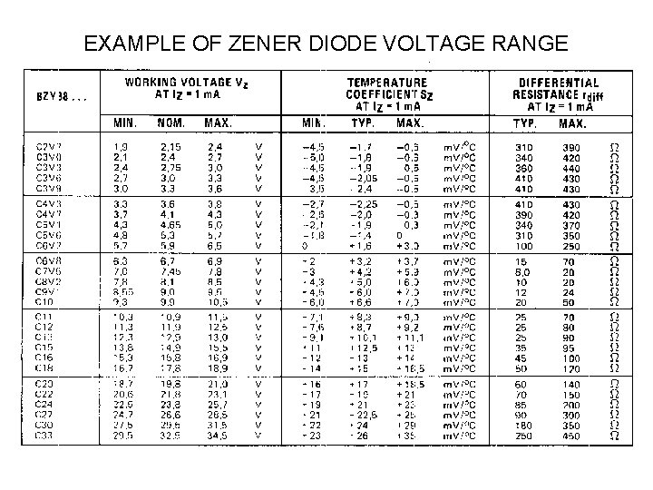
EXAMPLE OF ZENER DIODE VOLTAGE RANGE
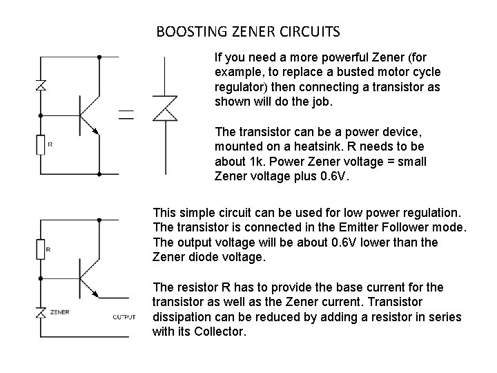
BOOSTING ZENER CIRCUITS If you need a more powerful Zener (for example, to replace a busted motor cycle regulator) then connecting a transistor as shown will do the job. The transistor can be a power device, mounted on a heatsink. R needs to be about 1 k. Power Zener voltage = small Zener voltage plus 0. 6 V. This simple circuit can be used for low power regulation. The transistor is connected in the Emitter Follower mode. The output voltage will be about 0. 6 V lower than the Zener diode voltage. The resistor R has to provide the base current for the transistor as well as the Zener current. Transistor dissipation can be reduced by adding a resistor in series with its Collector.
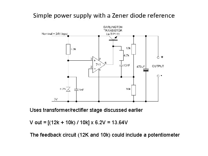
Simple power supply with a Zener diode reference Uses transformer/rectifier stage discussed earlier V out = [(12 k + 10 k) / 10 k] x 6. 2 V = 13. 64 V The feedback circuit (12 K and 10 k) could include a potentiometer
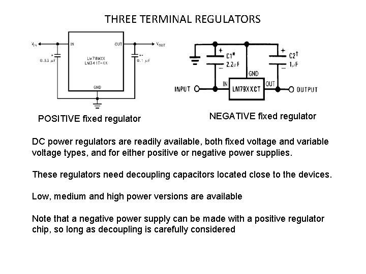
THREE TERMINAL REGULATORS POSITIVE fixed regulator NEGATIVE fixed regulator DC power regulators are readily available, both fixed voltage and variable voltage types, and for either positive or negative power supplies. These regulators need decoupling capacitors located close to the devices. Low, medium and high power versions are available Note that a negative power supply can be made with a positive regulator chip, so long as decoupling is carefully considered
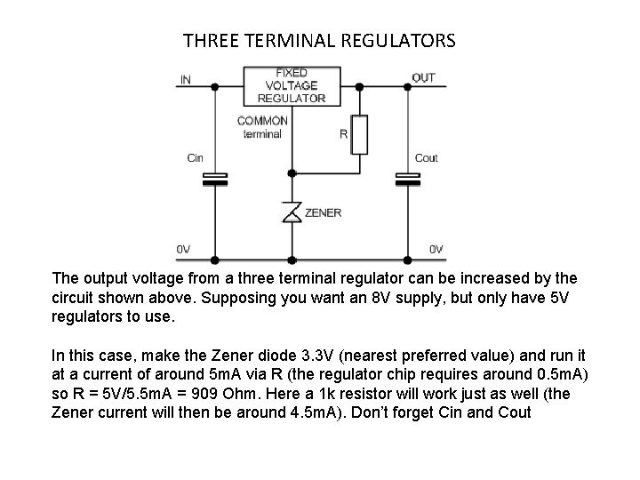
THREE TERMINAL REGULATORS The output voltage from a three terminal regulator can be increased by the circuit shown above. Supposing you want an 8 V supply, but only have 5 V regulators to use. In this case, make the Zener diode 3. 3 V (nearest preferred value) and run it at a current of around 5 m. A via R (the regulator chip requires around 0. 5 m. A) so R = 5 V/5. 5 m. A = 909 Ohm. Here a 1 k resistor will work just as well (the Zener current will then be around 4. 5 m. A). Don’t forget Cin and Cout
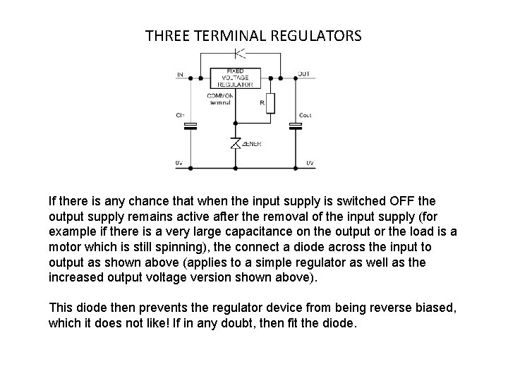
THREE TERMINAL REGULATORS If there is any chance that when the input supply is switched OFF the output supply remains active after the removal of the input supply (for example if there is a very large capacitance on the output or the load is a motor which is still spinning), the connect a diode across the input to output as shown above (applies to a simple regulator as well as the increased output voltage version shown above). This diode then prevents the regulator device from being reverse biased, which it does not like! If in any doubt, then fit the diode.
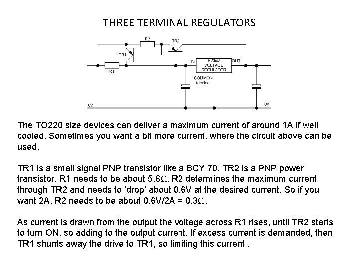
THREE TERMINAL REGULATORS The TO 220 size devices can deliver a maximum current of around 1 A if well cooled. Sometimes you want a bit more current, where the circuit above can be used. TR 1 is a small signal PNP transistor like a BCY 70. TR 2 is a PNP power transistor. R 1 needs to be about 5. 6 W. R 2 determines the maximum current through TR 2 and needs to ‘drop’ about 0. 6 V at the desired current. So if you want 2 A, R 2 needs to be about 0. 6 V/2 A = 0. 3 W. As current is drawn from the output the voltage across R 1 rises, until TR 2 starts to turn ON, so adding to the output current. If excess current is demanded, then TR 1 shunts away the drive to TR 1, so limiting this current.
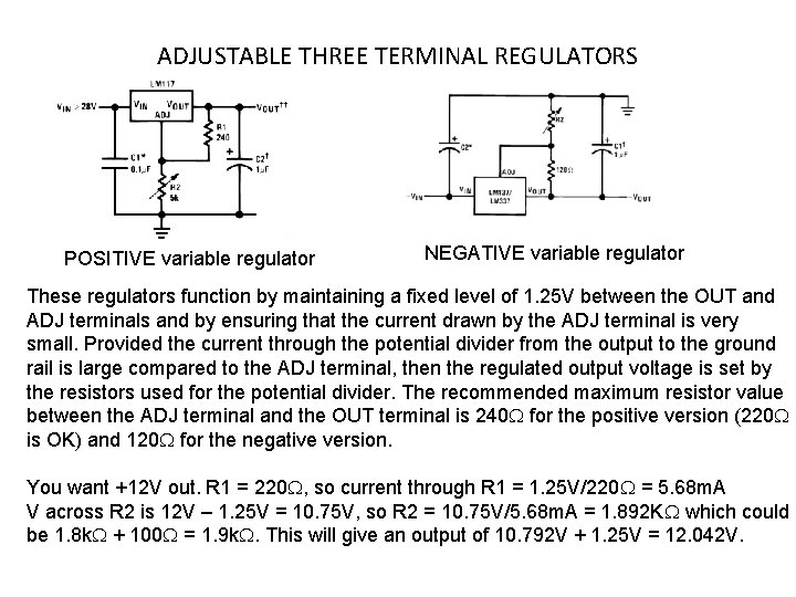
ADJUSTABLE THREE TERMINAL REGULATORS POSITIVE variable regulator NEGATIVE variable regulator These regulators function by maintaining a fixed level of 1. 25 V between the OUT and ADJ terminals and by ensuring that the current drawn by the ADJ terminal is very small. Provided the current through the potential divider from the output to the ground rail is large compared to the ADJ terminal, then the regulated output voltage is set by the resistors used for the potential divider. The recommended maximum resistor value between the ADJ terminal and the OUT terminal is 240 W for the positive version (220 W is OK) and 120 W for the negative version. You want +12 V out. R 1 = 220 W, so current through R 1 = 1. 25 V/220 W = 5. 68 m. A V across R 2 is 12 V – 1. 25 V = 10. 75 V, so R 2 = 10. 75 V/5. 68 m. A = 1. 892 KW which could be 1. 8 k. W + 100 W = 1. 9 k. W. This will give an output of 10. 792 V + 1. 25 V = 12. 042 V.
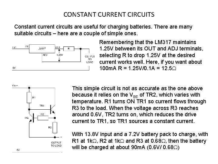
CONSTANT CURRENT CIRCUITS Constant current circuits are useful for charging batteries. There are many suitable circuits – here a couple of simple ones. Remembering that the LM 317 maintains 1. 25 V between its OUT and ADJ terminals, selecting R to drop 1. 25 V at the desired current works well. Here, if you want about 100 m. A R = 1. 25 V/0. 1 A = 12. 5 W This simple circuit is not as accurate as the one above because it relies on the VBE of TR 2, which varies with temperature. R 1 turns ON TR 1 so current flows through R 3 to the load. When the voltage across R 3 reaches around 0. 6 V, TR 2 turns on, which reduces the drive current to TR 1, so TR 1 sources a constant current. With 13. 8 V input and a 7. 2 V battery pack to charge, with R 1 at 1 k. W, R 2 at 1 k. W and R 3 at 0. 68 W, then the battery will be charged at about 90 m. A (0. 6 V/ 0. 68 W)
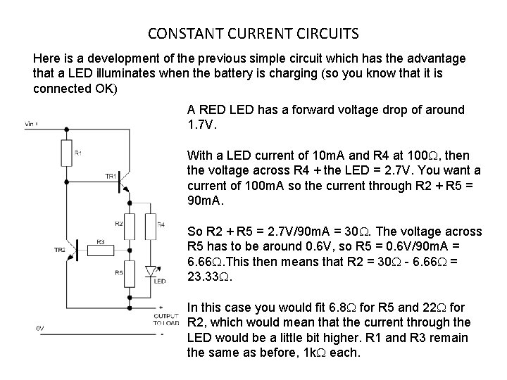
CONSTANT CURRENT CIRCUITS Here is a development of the previous simple circuit which has the advantage that a LED illuminates when the battery is charging (so you know that it is connected OK) A RED LED has a forward voltage drop of around 1. 7 V. With a LED current of 10 m. A and R 4 at 100 W, then the voltage across R 4 + the LED = 2. 7 V. You want a current of 100 m. A so the current through R 2 + R 5 = 90 m. A. So R 2 + R 5 = 2. 7 V/90 m. A = 30 W. The voltage across R 5 has to be around 0. 6 V, so R 5 = 0. 6 V/90 m. A = 6. 66 W. This then means that R 2 = 30 W - 6. 66 W = 23. 33 W. In this case you would fit 6. 8 W for R 5 and 22 W for R 2, which would mean that the current through the LED would be a little bit higher. R 1 and R 3 remain the same as before, 1 k. W each.
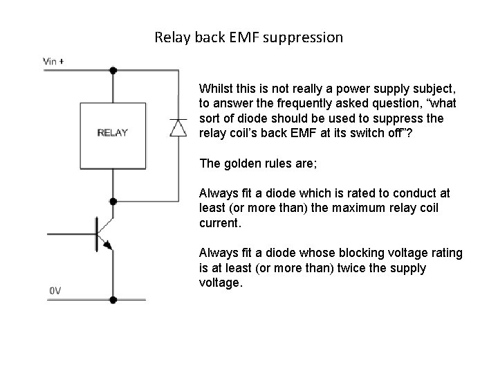
Relay back EMF suppression Whilst this is not really a power supply subject, to answer the frequently asked question, “what sort of diode should be used to suppress the relay coil’s back EMF at its switch off”? The golden rules are; Always fit a diode which is rated to conduct at least (or more than) the maximum relay coil current. Always fit a diode whose blocking voltage rating is at least (or more than) twice the supply voltage.
- Slides: 28