Introduction to 80386 Internal Architecture of 80386 Introduction


 4 Gbytes b) 6 Mbytes c) 4")
- Slides: 31
Introduction to 80386 Internal Architecture of 80386 Introduction to 80486 Internal Architecture of 80486 R. Sivaranjani , Asst professor, D. Mythili, Asst professor, Department of Computer Technology
Module 8 learning unit 18 Architecture of 80386 • The Internal Architecture of 80386 is divided into 3 sections. • Central processing unit • Memory management unit • Bus interface unit • Central processing unit is further divided into Execution unit and Instruction unit • Execution unit has 8 General purpose and 8 Special purpose registers which are either used for handling data or calculating offset addresses.
• The Instruction unit decodes the opcode bytes received from the 16 -byte instruction code queue and arranges them in a 3 - instruction decoded instruction queue. • After decoding them pass it to the control section for deriving the necessary control signals. The barrel shifter increases the speed of all shift and rotate operations. • The multiply / divide logic implements the bit-shift-rotate algorithms to complete the operations in minimum time. • Even 32 - bit multiplications can be executed within one microsecond by the multiply / divide logic. • The Memory management unit consists of a Segmentation unit and a Paging unit. • Segmentation unit allows the use of two address components, viz. segment and offset for relocability and sharing of code and data. • Segmentation unit allows segments of size 4 Gbytes at max. • The Paging unit organizes the physical memory in terms of pages of 4 kbytes size each. • Paging unit works under the control of the segmentation unit, i. e. each segment is further divided into pages. The virtual memory is also organizes in terms of segments and pages by the memory management unit. • The Segmentation unit provides a 4 level protection mechanism for protecting and isolating the system code and data from those of the application program. • Paging unit converts linear addresses into physical addresses. • The control and attribute PLA checks the privileges at the page level. Each of the pages maintains the paging information of the task. The limit and attribute PLA checks segment limits and attributes at segment level to avoid invalid accesses to code and data in the memory segments. • The Bus control unit has a prioritizer to resolve the priority of the various bus requests. This controls the access of the bus. The address driver drives the bus enable and address signal A 0 – A 31. The pipeline and dynamic bus sizing unit handle the related control signals. • The data buffers interface the internal data bus with the system bus.
A VCC B VSS C D A 8 A 11 E A 14 F A 15 G A 16 H J K L M A 17 A 20 A 21 A 23 A 26 N P A 27 A 30 1 1 VSS A 5 A 7 A 10 A 13 VSS VCC A 18 VSS A 22 A 24 A 29 A 31 VCC 2 2 A 3 A 4 A 6 A 9 A 12 VSS VCC A 19 VSS A 25 A 28 A 17 VSS A 30 3 3 NC NC VSS A 2 VCC D 29 4 4 VCC VSS D 31 VCC D 27 D 26 5 5 VSS NC NC VCC INTR D 28 D 25 VSS VCC D 24 VSS D 23 6 NC 7 6 7 ERROR# NMI PEREQ METAL LID VCC 8 8 VSS D 20 BUSY# RESET D 21 D 22 9 9 VCC W/R# LOCK# VSS D 17 D 19 10 10 D/C# VSS D 15 VSS D 16 D 18 11 11 M/IO# NC VCC BED# CLK 2 VCC D 0 VSS D 7 VCC D 10 D 12 D 14 12 12 BE 3# BE 2# BE 1# NA# NC NC READY# D 1 VSS D 5 D 8 VCC D 11 D 13 13 13 VCC VSS BS 16# HOLD ADS# VSS VCC D 2 D 3 D 4 D 6 HLDA D 9 VSS 14 14 A B C D E F G H PIN DIAGRAM OF 80386 J K L M N P
Signal Descriptions of 80386 • CLK 2 : The input pin provides the basic system clock timing for the operation of 80386. • D 0 – D 31: These 32 lines act as bidirectional data bus during different access cycles. • A 31 – A 2: These are upper 30 bit of the 32 - bit address bus. • BE 0 to BE 3 : The 32 - bit data bus supported by 80386 and the memory system of 80386 can be viewed as a 4 - byte wide memory access mechanism. The 4 byte enable lines BE 0 to BE 3 , may be used for enabling these 4 blanks. Using these 4 enable signal lines, the CPU may transfer 1 byte / 2 / 3 / 4 byte of data simultaneously. • ADS#: The address status output pin indicates that the address bus and bus cycle definition pins( W/R#, D/C#, M/IO#, BE 0# to BE 3# ) are carrying the respective valid signals. The 80383 does not have any ALE signals and so this signals may be used for latching the address to external latches. • READY#: The ready signals indicates to the CPU that the previous bus cycle has been terminated and the bus is ready for the next cycle. The signal is used to insert WAIT states in a bus cycle and is useful for interfacing of slow devices with CPU. • VCC: These are system power supply lines. • VSS: These return lines for the power supply. • BS 16#: The bus size – 16 input pin allows the interfacing of 16 bit devices with the 32 bit wide 80386 data bus. Successive 16 bit bus cycles may be executed to read a 32 bit data from a peripheral. • HOLD: The bus hold input pin enables the other bus masters to gain control of the system bus if it is asserted. • HLDA: The bus hold acknowledge output indicates that a valid bus hold request has been received and the bus has been relinquished by the CPU. • BUSY#: The busy input signal indicates to the CPU that the coprocessor is busy with the allocated task. • ERROR#: The error input pin indicates to the CPU that the coprocessor has encountered an error while executing its instruction. • PEREQ: The processor extension request output signal indicates to the CPU to fetch a data word for the coprocessor. • INTR: This interrupt pin is a maskable interrupt, that can be masked using the IF of the flag register. • NMI: A valid request signal at the non-maskable interrupt request input pin internally generates a non- maskable interrupt of type 2. • RESET: A high at this input pin suspends the current operation and restart the execution from the starting location. • N / C : No connection pins are expected to be left open while connecting the 80386 in the circuit.
D 0 D 1 D 2 D 3 D 4 D 5 D 6 D 7 D 8 D 9 D 10 D 11 D 12 BE 0 BE 1 BE 2 BE 3 A 2 A 3 A 4 A 5 A 6 A 7 A 8 A 9 A 10 D 13 D 14 D 15 D 16 D 17 D 18 D 19 D 20 D 21 D 22 D 23 A 11 A 12 A 13 A 14 A 15 A 16 A 17 A 18 A 19 A 20 A 21 D 24 D 25 D 26 D 27 D 28 D 29 D 30 D 31 ADS NA BS 16 READY 80386 DX A 22 A 23 A 24 A 25 A 26 A 27 A 28 A 29 A 30 A 31 W/R D /C M / IO HOLDA INTR NMI RESET CLK 2 LOCK PEREQ BUSY ERROR
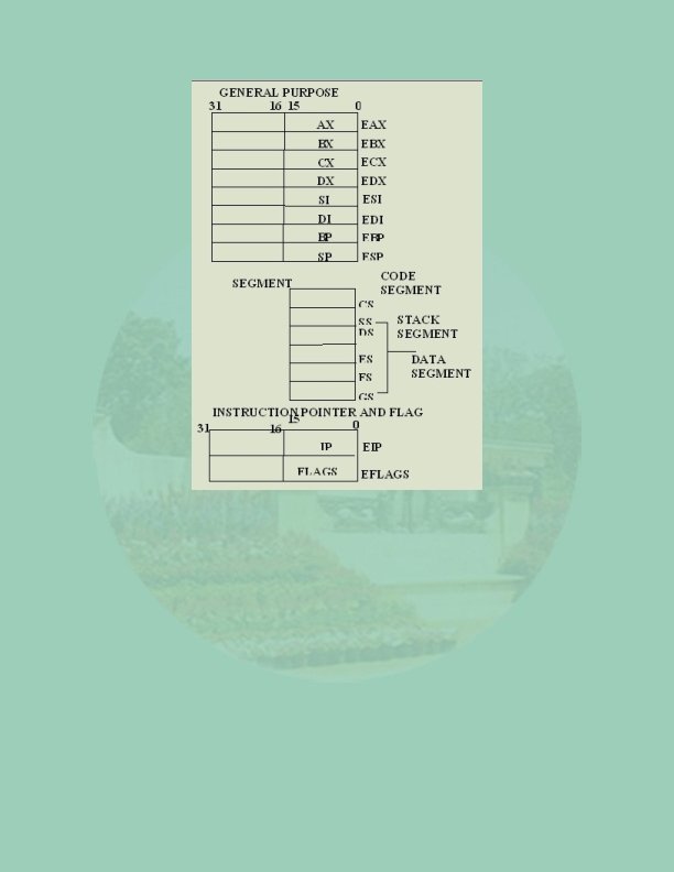
Register Organisation • The 80386 has eight 32 - bit general purpose registers which may be used as either 8 bit or 16 bit registers. • A 32 - bit register known as an extended register, is represented by the register name with prefix E. • Example : A 32 bit register corresponding to AX is EAX, similarly BX is EBX etc. • The 16 bit registers BP, SI and DI in 8086 are now available with their extended size of 32 bit and are names as EBP, ESI and EDI. • AX represents the lower 16 bit of the 32 bit register EAX. • BP, SI, DI represents the lower 16 bit of their 32 bit counterparts, and can be used as independent 16 bit registers. • The six segment registers available in 80386 are CS, SS, DS, ES, FS and GS. • The CS and SS are the code and the stack segment registers respectively, while DS, ES, FS, GS are 4 data segment registers. • A 16 bit instruction pointer IP is available along with 32 bit counterpart EIP.
• Flag Register of 80386: The Flag register of 80386 is a 32 bit register. Out of the 32 bits, Intel has reserved bits D 18 to D 31, D 5 and D 3, while D 1 is always set at 1. Two extra new flags are added to the 80286 flag to derive the flag register of 80386. They are VM and RF flags. • VM - Virtual Mode Flag: If this flag is set, the 80386 enters the virtual 8086 mode within the protection mode. This is to be set only when the 80386 is in protected mode. In this mode, if any privileged instruction is executed an exception 13 is generated. This bit can be set using IRET instruction or any task switch operation only in the protected mode.
• RF- Resume Flag: This flag is used with the debug register breakpoints. It is checked at the starting of every instruction cycle and if it is set, any debug fault is ignored during the instruction cycle. The RF is automatically reset after successful execution of every instruction, except for IRET and POPF instructions. • Also, it is not automatically cleared after the successful execution of JMP, CALL and INT instruction causing a task switch. These instruction are used to set the RF to the value specified by the memory data available at the stack. • Segment Descriptor Registers: This registers are not available for programmers, rather they are internally used to store the descriptor information, like attributes, limit and base addresses of segments. • The six segment registers have corresponding six 73 bit descriptor registers. Each of them contains 32 bit base address, 32 bit base limit and 9 bit attributes. These are automatically loaded when the corresponding segments are loaded with selectors. • Control Registers: The 80386 has three 32 bit control registers CR 0, CR 2 and CR 3 to hold global machine status independent of the executed task. Load and store instructions are available to access these registers. • System Address Registers: Four special registers are defined to refer to the descriptor tables supported by 80386. • The 80386 supports four types of descriptor table, viz. global descriptor table (GDT), interrupt descriptor table (IDT), local descriptor table (LDT) and task state segment descriptor (TSS). • Debug and Test Registers: Intel has provide a set of 8 debug registers for hardware debugging. Out of these eight registers DR 0 to DR 7, two registers DR 4 and DR 5 are Intel reserved. • The initial four registers DR 0 to DR 3 store four program controllable breakpoint addresses, while DR 6 and DR 7 respectively hold breakpoint status and breakpoint control information. • Two more test register are provided by 80386 for page cacheing namely test control and test status register. • ADDRESSING MODES: The 80386 supports overall eleven addressing modes to facilitate efficient execution of higher level language programs. • In case of all those modes, the 80386 can now have 32 -bit immediate or 32 - bit register operands or displacements. • The 80386 has a family of scaled modes. In case of scaled modes, any of the index register values can be multiplied by a valid scale factor to obtain the displacement. • The valid scale factor are 1, 2, 4 and 8. • The different scaled modes are as follows. • Scaled Indexed Mode: Contents of the an index register are multiplied by a scale factor that may be added further to get the operand offset. • Based Scaled Indexed Mode: Contents of the an index register are multiplied by a scale factor and then added to base register to obtain the offset. • Based Scaled Indexed Mode with Displacement: The Contents of the an index register are multiplied by a scaling factor and the result is added to a base register and a displacement to get the offset of an operand.
Real Address Mode of 80386 • After reset, the 80386 starts from memory location FFFFFFF 0 H under the real address mode. In the real mode, 80386 works as a fast 8086 with 32 -bit registers and data types. • In real mode, the default operand size is 16 bit but 32 - bit operands and addressing modes may be used with the help of override prefixes. • The segment size in real mode is 64 k, hence the 32 -bit effective addressing must be less than 0000 FFFFFH. The real mode initializes the 80386 and prepares it for protected mode. • Memory Addressing in Real Mode: In the real mode, the 80386 can address at the most 1 Mbytes of physical memory using address lines A 0 -A 19. • Paging unit is disabled in real addressing mode, and hence the real addresses are the same as the physical addresses. • To form a physical memory address, appropriate segment registers contents (16 -bits) are shifted left by four positions and then added to the 16 -bit offset address formed using one of the addressing modes, in the same way as in the 80386 real address mode. • The segment in 80386 real mode can be read, write or executed, i. e. no protection is available. • Any fetch or access past the end of the segment limit generate exception 13 in real address mode. • The segments in 80386 real mode may be overlapped or non-overlapped. • The interrupt vector table of 80386 has been allocated 1 Kbyte space starting from 00000 H to 003 FFH.
Protected Mode of 80386 • All the capabilities of 80386 are available for utilization in its protected mode of operation. • The 80386 in protected mode support all the software written for 80286 and 8086 to be executed under the control of memory management and protection abilities of 80386. • The protected mode allows the use of additional instruction, addressing modes and capabilities of 80386. • ADDRESSING IN PROTECTED MODE: In this mode, the contents of segment registers are used as selectors to address descriptors which contain the segment limit, base address and access rights byte of the segment. • The effective address (offset) is added with segment base address to calculate linear address. This linear address is further used as physical address, if the paging unit is disabled, otherwise the paging unit converts the linear address into physical address. • The paging unit is a memory management unit enabled only in protected mode. The paging mechanism allows handling of large segments of memory in terms of pages of 4 Kbyte size. • The paging unit operates under the control of segmentation unit. The paging unit if enabled converts linear addresses into physical address, in protected mode.
Segmentation • DESCRIPTOR TABLES: These descriptor tables and registers are manipulated by the operating system to ensure the correct operation of the processor, and hence the correct execution of the program. • Three types of the 80386 descriptor tables are listed as follows: • GLOBAL DESCRIPTOR TABLE ( GDT ) • LOCAL DESCRIPTOR TABLE ( LDT ) • INTERRUPT DESCRIPTOR TABLE ( IDT ) • DESCRIPTORS: The 80386 descriptors have a 20 -bit segment limit and 32 -bit segment address. The descriptor of 80386 are 8 -byte quantities access right or attribute bits along with the base and limit of the segments. • Descriptor Attribute Bits: The A (accessed) attributed bit indicates whether the segment has been accessed by the CPU or not. • The TYPE field decides the descriptor type and hence the segment type. • The S bit decides whether it is a system descriptor (S=0) or code/data segment descriptor ( S=1). • The DPL field specifies the descriptor privilege level. • The D bit specifies the code segment operation size. If D=1, the segment is a 32 -bit operand segment, else, it is a 16 -bit operand segment. • The P bit (present) signifies whether the segment is present in the physical memory or not. If P=1, the segment is present in the physical memory. • The G (granularity) bit indicates whether the segment is page addressable. The zero bit must remain zero for compatibility with future process. • The AVL (available) field specifies whether the descriptor is for user or for operating system. • The 80386 has five types of descriptors listed as follows: 1. Code or Data Segment Descriptors. 2. System Descriptors. 3. Local descriptors. 4. TSS (Task State Segment) Descriptors. 5. GATE Descriptors. • The 80386 provides a four level protection mechanism exactly in the same way as the 80286 does.
Paging • PAGING OPERATION: Paging is one of the memory management techniques used for virtual memory multitasking operating system. • The segmentation scheme may divide the physical memory into a variable size segments but the paging divides the memory into a fixed size pages. • The segments are supposed to be the logical segments of the program, but the pages do not have any logical relation with the program. • The pages are just fixed size portions of the program module or data. • The advantage of paging scheme is that the complete segment of a task need not be in the physical memory at any time. • Only a few pages of the segments, which are required currently for the execution need to be available in the physical memory. Thus the memory requirement of the task is substantially reduced, relinquishing the available memory for other tasks. • Whenever the other pages of task are required for execution, they may be fetched from the secondary storage. • The previous page which are executed, need not be available in the memory, and hence the space occupied by them may be relinquished for other tasks. • Thus paging mechanism provides an effective technique to manage the physical memory for multitasking systems.
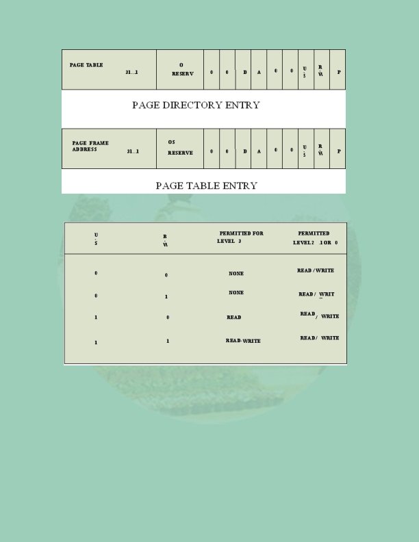
• Paging Unit: The paging unit of 80386 uses a two level table mechanism to convert a linear address provided by segmentation unit into physical addresses. • The paging unit converts the complete map of a task into pages, each of size 4 K. The task is further handled in terms of its page, rather than segments. • The paging unit handles every task in terms of three components namely page directory, page tables and page itself. • Paging Descriptor Base Register: The control register CR 2 is used to store the 32 -bit linear address at which the previous page fault was detected. • The CR 3 is used as page directory physical base address register, to store the physical starting address of the page directory. • The lower 12 bit of the CR 3 are always zero to ensure the page size aligned directory. A move operation to CR 3 automatically loads the page table entry caches and a task switch operation, to load CR 0 suitably. • Page Directory : This is at the most 4 Kbytes in size. Each directory entry is of 4 bytes, thus a total of 1024 entries are allowed in a directory. • The upper 10 bits of the linear address are used as an index to the corresponding page directory entry. The page directory entries point to page tables. • Page Tables: Each page table is of 4 Kbytes in size and many contain a maximum of 1024 entries. The page table entries contain the starting address of the page and the statistical information about the page. • The upper 20 bit page frame address is combined with the lower 12 bit of the linear address. The address bits A 12 - A 21 are used to select the 1024 page table entries. The page table can be shared between the tasks. • The P bit of the above entries indicate, if the entry can be used in address translation. • If P=1, the entry can be used in address translation, otherwise it cannot be used. • The P bit of the currently executed page is always high. • The accessed bit A is set by 80386 before any access to the page. If A=1, the page is accessed, else unaccessed. • The D bit ( Dirty bit) is set before a write operation to the page is carried out. The D-bit is undefined for page director entries. • The OS reserved bits are defined by the operating system software. • The User / Supervisor (U/S) bit and read/write bit are used to provide protection. These bits are decoded to provide protection under the 4 level protection model. • The level 0 is supposed to have the highest privilege, while the level 3 is supposed to have the least privilege. • This protection provide by the paging unit is transparent to the segmentation unit.
Virtual 8086 Mode • In its protected mode of operation, 80386 DX provides a virtual 8086 operating environment to execute the 8086 programs. • The real mode can also used to execute the 8086 programs along with the capabilities of 80386, like protection and a few additional instructions. • Once the 80386 enters the protected mode from the real mode, it cannot return back to the real mode without a reset operation. • Thus, the virtual 8086 mode of operation of 80386, offers an advantage of executing 8086 programs while in protected mode. • The address forming mechanism in virtual 8086 mode is exactly identical with that of 8086 real mode. • In virtual mode, 8086 can address 1 Mbytes of physical memory that may be anywhere in the 4 Gbytes address space of the protected mode of 80386. • Like 80386 real mode, the addresses in virtual 8086 mode lie within 1 Mbytes of memory. • In virtual mode, the paging mechanism and protection capabilities are available at the service of the programmers. • The 80386 supports multiprogramming, hence more than one programmer may be use the CPU at a time.
• Paging unit may not be necessarily enable in virtual mode, but may be needed to run the 8086 programs which require more than 1 Mbyts of memory for memory management function. • In virtual mode, the paging unit allows only 256 pages, each of 4 Kbytes size. • Each of the pages may be located anywhere in the maximum 4 Gbytes physical memory. The virtual mode allows the multiprogramming of 8086 applications. • The virtual 8086 mode executes all the programs at privilege level 3. Any of the other programmes may deny access to the virtual mode programs or data. • However, the real mode programs are executed at the highest privilege level, i. e. level 0. • The virtual mode may be entered using an IRET instruction at CPL=0 or a task switch at any CPL, executing any task whose TSS is having a flag image with VM flag set to 1. • The IRET instruction may be used to set the VM flag and consequently enter the virtual mode. • The PUSHF and POPF instructions are unable to read or set the VM bit, as they do not access it. • Even in the virtual mode, all the interrupts and exceptions are handled by the protected mode interrupt handler. • To return to the protected mode from the virtual mode, any interrupt or execution may be used. • As a part of interrupt service routine, the VM bit may be reset to zero to pull back the 80386 into protected mode.
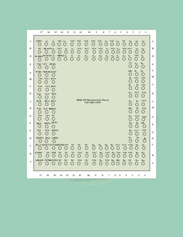
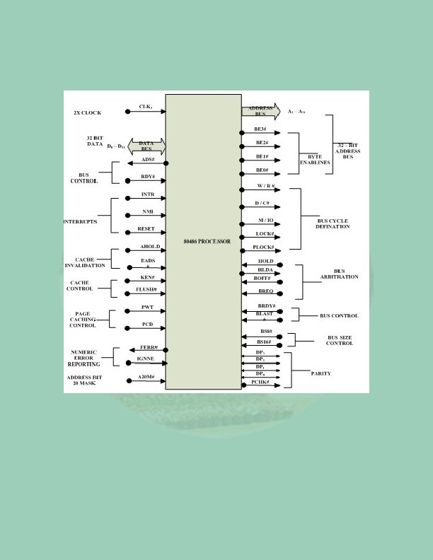
Summary of 80386 • This 80386 is a 32 bit processor that supports, 8 bit/32 bit data operands. • The 80386 instruction set is upward compatible with all its predecessors. • The 80386 can run 8086 applications under protected mode in its virtual 8086 mode of operation. • With the 32 bit address bus, the 80386 can address upto 4 Gbytes of physical memory. The physical memory is organised in terms of segments of 4 Gbytes at maximum. • The 80386 CPU supports 16 K number of segments and thus the total virtual space of 4 Gbytes * 16 K = 64 Terrabytes. • The memory management section of 80386 supports the virtual memory, paging and four levels of protection, maintaining full compatibility with 80286. • The 80386 offers a set of 8 debug registers DR 0 -DR 7 for hardware debugging and control. The 80386 has on-chip address translation cache. • The concept of paging is introduced in 80386 that enables it to organise the available physical memory in terms of pages of size 4 Kbytes each, under the segmented memory. • The 80386 can be supported by 80387 for mathematical data processing. 80486 Microprocessor • The 32 -bit 80486 is the next evolutionary step up from the 80386. • One of the most obvious feature included in a 80486 is a built in math coprocessor. This coprocessor is essentially the same as the 80387 processor used with a 80386, but being integrated on the chip allows it to execute math instructions about three times as fast as a 80386/387 combination. • 80486 is an 8 Kbyte code and data cache. • To make room for the additional signals, the 80486 is packaged in a 168 pin, pin grid array package instead of the 132 pin PGA used for the 80386. Pin Definitions • A 31 -A 2 : Address outputs A 31 -A 2 provide the memory and I/O with the address during normal operation. During a cache line invalidation A 31 -A 4 are used to drive the microprocessor. • A 20 M 3 : The address bit 20 mask causes the 80486 to wrap its address around from location 000 FFFFFH to 0000 H as in 8086. This provides a memory system that functions like the 1 M byte real memory system in the 8086 processors. • ADS : The address data strobe become logic zero to indicate that the address bus contains a valid memory address.
• AHOLD: The address hold input causes the microprocessor to place its address bus connections at their high-impedance state, with the remainder of the buses staying active. It is often used by another bus master to gain access for a cache invalidation cycle. • BREQ: This bus request output indicates that the 486 has generated an internal bus request. • BE 3 - BE 0 : Byte enable outputs select a bank of the memory system when information is transferred between the microprocessor and its memory and I/O. The BE 3 signal enables D 31 – D 24 , BE 2 enables D 23 -D 16, BE 1 enables D 15 – D 8 and BE 0 enables D 7 -D 0. • BLAST : The burst last output shows that the burst bus cycle is complete on the next activation of BRDY# signal.
• BOFF : The Back-off input causes the microprocessor to place its buses at their high impedance state during the next cycle. The microprocessor remains in the bus hold state until the BOFF# pin is placed at a logic 1 level. • NMI : The non-maskable interrupt input requests a type 2 interrupt. • BRDY : The burst ready input is used to signal the microprocessor that a burst cycle is complete. • KEN : The cache enable input causes the current bus to be stored in the internal. • LOCK : The lock output becomes a logic 0 for any instruction that is prefixed with the lock prefix. • W / R : current bus cycle is either a read or a write. • IGNNE : The ignore numeric error input causes the coprocessor to ignore floating point error and to continue processing data. The signal does not affect the state of the FERR pin. • FLUSH : The cache flush input forces the microprocessor to erase the contents of its 8 K byte internal cache. • EADS : The external address strobe input is used with AHOLD to signal that an external address is used to perform a cache invalidation cycle. • FERR : The floating point error output indicates that the floating point coprocessor has detected an error condition. It is used to maintain compatibility with DOS software. • BS 8 : The bus size 8, input causes the 80486 to structure itself with an 8 -bit data bus to access byte-wide memory and I/O components. • BS 16 : The bus size 16, input causes the 80486 to structure itself with an 16 -bit data bus to access word-wide memory and I/O components. • PCHK : The parity check output indicates that a parity error was detected during a read operation on the DP 3 – DP 0 pin. • PLOCK : The pseudo-lock output indicates that current operation requires more than one bus cycle to perform. This signal becomes a logic 0 for arithmetic coprocessor operations that access 64 or 80 bit memory data.
• PWT: The page write through output indicates the state of the PWT attribute bit in the page table entry or the page directory entry. • RDY : The ready input indicates that a non-burst bus cycle is complete. The RDY signal must be returned or the microprocessor places wait states into its timing until RDY is asserted. • M / IO : Memory / IO# defines whether the address bus contains a memory address or an I/O port number. It is also combined with the W/ R signal to generate memory and I/O read and write control signals. 80486 Signal Group • The 80486 data bus, address bus, byte enable, ADS#, RDY#, INTR, RESET, NMI, M/IO#, D/C#, W/R#, LOCK#, HOLD, HLDA and BS 16# signals function as we described for 80386. • The 80486 requires 1 clock instead of 2 clock required by 80386. • A new signal group on the 486 is the PARITY group DP 0 -DP 3 and PCHK#. • These signals allow the 80486 to implement parity detection / generation for memory reads and memory writes. • During a memory write operation, the 80486 generates an even parity bit for each byte and outputs these bits on the DP 0 -DP 3 lines. • These bits will store in a separate parity memory bank. • During a read operation the stored parity bits will be read from the parity memory and applied to the DP 0 -DP 3 pins. • The 80486 checks the parities of the data bytes read and compares them with the DP 0 DP 3 signals. If a parity error is found, the 80486 asserts the PCHK# signal. • Another new signals group consists of the BURST ready signal BRDY# and BURST last signal BLAST#. • These signals are used to control burst-mode memory reads and writes. • A normal 80486 memory read operation to read a line into the cache requires 2 clock cycles. However, if a series of reads is being done from successive memory locations, the reads can be done in burst mode with only 1 clock cycle per read. • To start the process the 80486 sends out the first address and asserts the BLAST# signal high. When the external DRAM controller has the first data bus, it asserts the BRDY# signal. • The 80486 reads the data word and outputs the next address. Since the data words are at successive addresses, only the lower address bits need to be changed. If the DRAM controller is operating in the page or the static column modes then it will only have to output a new column address to the DRAM. • In this mode the DRAM will be able to output the new data word within 1 clock cycle.
• When the processor has read the required number of data words, it asserts the BLAST# signal low to terminate the burst mode. • The final signal we want to discuss here are the bus request output signal BREQ, the back-off input signal BOFF#, the HOLD signal and the hold-acknowledge signal HLDA. • These signals are used to control sharing the local 486 bus by multiple processors ( bus master). • When a master on the bus need to use the bus, it asserts its BERQ signal. • An external parity circuit will evaluate requests to use the bus and grant bus use to the highest – priority master. To ask the 486 to release the bus , the bus controller asserts the 486 HOLD input or BOFF# input. • If the HOLD input is asserted, the 486 will finish the current bus cycle, float its buses and assert the HLDA signal. • To prevent another master from taking over the bus during a critical operation, the 486 can assert its LOCK# or PLOCK# signal. EFLAG Register of The 80486 • The extended flag register EFLAG is illustrated in the figure. The only new flag bit is the AC alignment check, used to indicate that the microprocessor has accessed a word at an odd address or a double word boundary. • Efficient software and execution require that data be stored at word or doubleword boundaries.
80486 Memory System • The memory system for the 486 is identical to 386 microprocessor. The 486 contains 4 G bytes of memory beginning at location 0000 H and ending at FFFFH. • The major change to the memory system is internal to 486 in the form of 8 K byte cache memory, which speeds the execution of instructions and the acquisition of data. • Another addition is the parity checker/ generator built into the 80486 microprocessor. • Parity Checker / Generator : Parity is often used to determine if data are correctly read from a memory location. INTEL has incorporated an internal parity generator / decoder. • Parity is generated by the 80486 during each write cycle. Parity is generated as even parity and a parity bit is provided for each byte of memory. The parity check bits appear on pins DP 0 -DP 3, which are also parity inputs as well as parity outputs. • These are typically stored in memory during each write cycle and read from memory during each read cycle. • On a read, the microprocessor checks parity and generates a parity check error, if it occurs on the PCHK# pin. A parity error causes no change in processing unless the user applies the PCHK signal to an interrupt input. • Interrupts are often used to signal a parity error in DS-based computer systems. This is same as 80386, except the parity bit storage. • If parity is not used, Intel recommends that the DP 0 – DP 3 pins be pulled up to +5 v.
• CACHE MEMORY: The cache memory system stores data used by a program and also the instructions of the program. The cache is organised as a 4 way set associative cache with each location containing 16 bytes or 4 doublewords of data. • Control register CR 0 is used to control the cache with two new control bits not present in the 80386 microprocessor. • The CD ( cache disable ) , NW ( non-cache write through ) bits are new to the 80486 and are used to control the 8 K byte cache. • If the CD bit is a logic 1, all cache operations are inhibited. This setting is only used for debugging software and normally remains cleared. The NW bit is used to inhibit cache write-through operation. As with CD, cache write through is inhibited only for testing. For normal operations CD = 0 and NW = 0. • Because the cache is new to 80486 microprocessor and the cache is filled using burst cycle not present on the 386.
80486 Memory Management • The 80486 contains the same memory-management system as the 80386. This includes a paging unit to allow any 4 K byte block of physical memory to be assigned to any 4 K byte block of linear memory. The only difference between 80386 and 80486 memorymanagement system is paging. • The 80486 paging system can disabled caching for section of translation memory pages, while the 80386 could not. • If these are compared with 80386 entries, the addition of two new control bits is observed ( PWT and PCD ). • The page write through and page cache disable bits control caching. • The PWT controls how the cache functions for a write operation of the external cache memory. It does not control writing to the internal cache. The logic level of this bit is found on the PWT pin of the 80486 microprocessor. Externally, it can be used to dictate the write through policy of the external caching. • The PCD bit controls the on-chip cache. If the PCD = 0, the on-chip cache is enabled for the current page of memory. • Note that 80386 page table entries place a logic 0 in the PCD bit position, enabling caching. If PCD = 1, the on-chip cache is disable. Caching is disable regard less of condition of KEN#, CD, and NW. Cache Test Registers • The 80486 cache test registers are TR 3, TR 4, TR 5. • Cache data register (TR 3) is used to access either the cache fill buffer for a write test operation or the cache read buffer for a cache read test operation. • In order to fill or read a cache line ( 128 bits wide ), TR 3 must be written or read four times. • The contents of the set select field in TR 5 determine which internal cache line is written or read through TR 3. The 7 bit test field selects one of the 128 different 16 byte wide cache lines. The entry select bits of TR 5 select an entry in the set or the 32 bit location in the read buffer.
• The control bits in TR 5 enable the fill buffer or read buffer operation ( 00 ) • Perform a cache write ( 01 ), Perform a cache read ( 10 ) • Flush the cache ( 11 ). • The cache status register (TR 4) hold the cache tag, LRU bits and a valid bit. This register is loaded with the tag and valid bit before a cache write operation and contains the tag, valid bit, LRU bits, and 4 valid bits on a cache test read. • Cache is tested each time that the microprocessor is reset if the AHOLD pin is high for 2 clocks prior to the RESET pin going low. This causes the 486 to completely test itself with a built in self test or BIST.
• The BIST uses TR 3, TR 4, TR 5 to completely test the internal cache. Its outcome is reported in register EAX. If EAX is a zero, the microprocessor, the coprocessor and cache have passed the self test. • The value of EAX can be tested after reset to determine if an error is detected. In most of the cases we do not directly access the test register unless we wish to perform our own tests on the cache or TLB.
1. Segmentation unit allows segments of a) 4 Gbytes b) 6 Mbytes c) 4 Mbytes size at maximum. d) 6 Gbytes 2. If input pin of 80386 if activated, allows address pipelining during 80386 bus cycles. a) BS 16 b) NA c) PEREQ d) ADS 3. Virtual Mode Flag bit can be set using instruction or any task switch operation only in the mode a) IRET, Virtual b) POPF, Real c) IRET, protected d) POPF, protected 4. The interrupt vector table of 80386 has been allocated space starting from to. a) 1 Kbyte, 00000 H, 003 FFH b) 2 Kbyte, 10000 H, 004 FFH c) 3 Kbyte, 01000 H, 007 FFH d) 4 Kbyte, 01000 H, 009 FFH 5. The bit decides whether it is a system descriptor or code/data segment descriptor a) P b) S c) D d) G 6. A new signal group on the 80486 is the a) PARITY b) DP 0 -DP 3 c) PCHK 7. . d) all is used to control the cache with two new control bits not present in the 80386 microprocessor. What are the bits used to control the 8 K byte cache? a) CR 0, CD, NW b) CR 0, NW, PWT c) Control Register Zero, PWT, PCD d) none 8. To prevent another master from taking over the bus during a critical operation, the 486 can assert its signal. a) LOCK# or PLOCK# b) HOLD or BOFF c) HLDA d) HOLD 9. 80386 support which type of descriptor table from the following? a) TDS b) ADS c) GDS d) MDS 10. 80386 support overall addressing modes to facilitate efficient execution of higher level language programs. a) 9 b) 10 c) 11 d) 12 Key: 8. 1 A 8. 2 B 8. 3 C 8. 4 A 8. 7 A 8. 8 A 8. 9 C 8. 10 C 8. 5 B 8. 6 D