Introduction 4 M Weisheit et al Science 315
 Pt Pt Fe.")
.")
")

 Ta (5 nm)")
/Mg. O/Fe(0. 3 nm)/Fe. B (1. 5 nm) /Ta/Ru Hex")
/Mg. O/Fe(0. 3 nm)/Fe. B (1. 5 nm) /Ta/Ru +V")


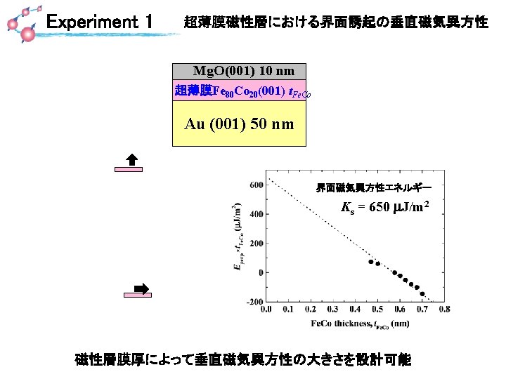
 t. Fe. Co: 0. 7 nm (in-plane) t.")
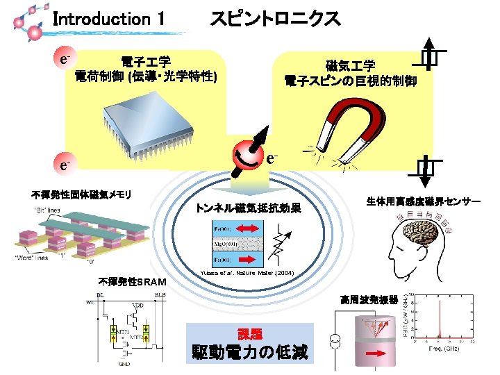
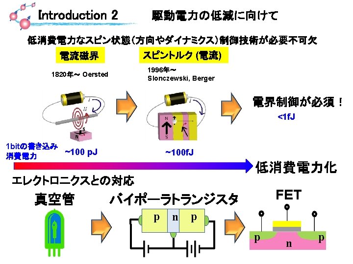
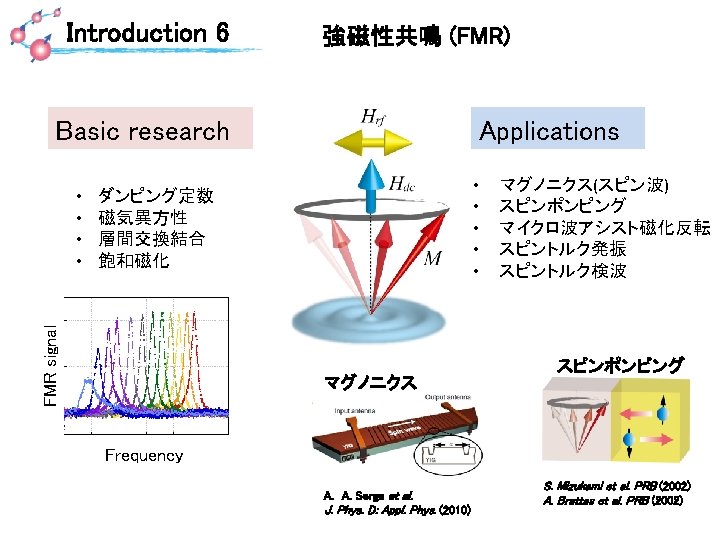
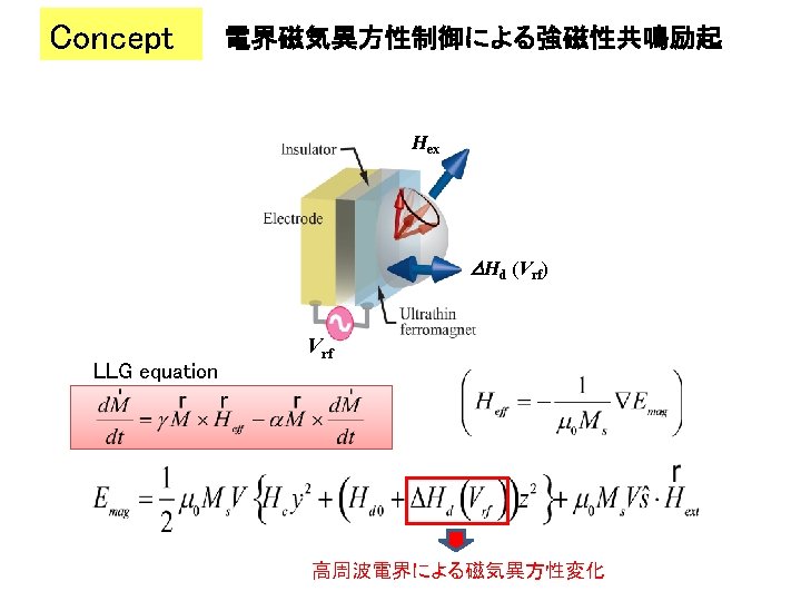
における電界磁気異方性を実現 電界による高速スピンダイナミクス(強磁性共鳴)励起を実証 電界パルスを用いたダイナミック磁化反転を実証 Voltage control of magnetic anisotropy Voltage-driven MRAM")


")
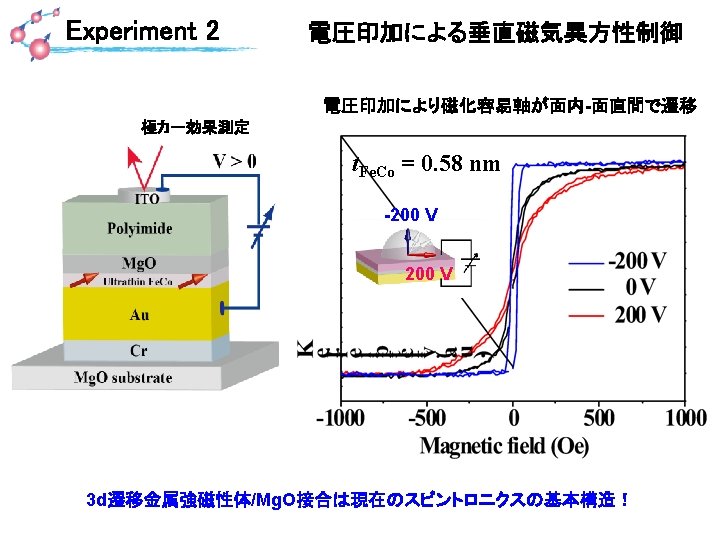
 Ref. Au / Fe 80 Co 20 (0. 4 nm)")

Pt, Fe(Co)Pd 白金族系の強いスピン-軌道相互作用を活用 2. 界面誘起の垂直磁気異方性 Mg.")


 Difference in the")


) ko")
.")
 g= -2. 3× 10⁵ m/(A sec) (g=2.")


- Slides: 46
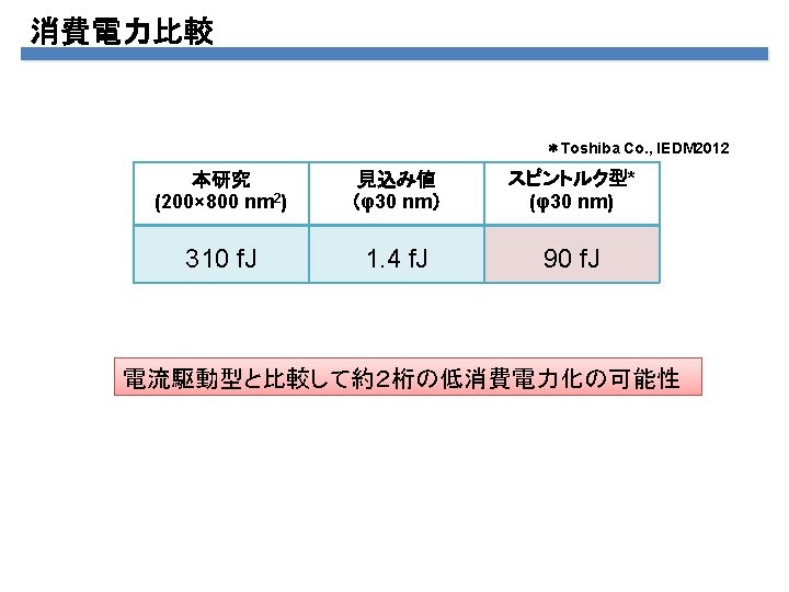
電界磁気異方性制御 Introduction 4 M. Weisheit et al. Science 315, 349 (2007) Pt Pt Fe. Pt Mg. O Electric double layer Electrolyte 1. 0 V -0. 12 -0. 11 H (T) -0. 1 0 H (T) 0. 1 Kerr rotation 0. 4 V 液体電界質による電気2重層の利用 4. 5%の保磁力変化 室温において、3 d遷移金属の垂直磁気異方性を 電界で制御することが可能!
Introduction 5 電界誘起磁気異方性変化の起源 -理論M. Tsujikawa and T. Oda, Phys. Rev. Lett. 102, 247203 (2009). Number of electrons Pt Fe Pt Electric field (V/Å)
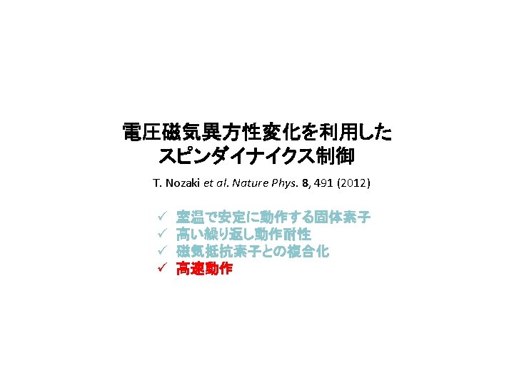
全固体素子における電圧磁気異方性制御の実現 T. Maruyama, Y. Shiota, T. N. et al. Nature Nanotech. 4, 158 (2009) Y. Shiota, T. N. et al. Appl. Phys. Exp. 2, 063001 (2009) T. Nozaki et al. APL. 96, 022506 (2010) Y. Shiota, T. N. et al. APEX 4, 043005 (2011) ü ü 室温で安定に動作する固体素子 高い繰り返し動作耐性 磁気抵抗素子との複合化 高速動作
様々な材料系における電界磁気異方性制御の報告例 Co. Fe. B Fe. Pd, Fe. Pt laser M. Endo et al. APL 96, 212503 (2010) K. Kita et al. APL 112, 033919 (2012) F. Bonell et al. APL 98, 232510 (2011) T. Seki et al. APL 98, 212505 (2011) Co. Cr. Pt-Ti. O 2 nanocomposite T. Zhou et al. APL 96, 012506 (2010)
トンネル磁気抵抗素子における電界磁気異方性制御 Junction size: 2 × 6 mm 2 Sputtering Ru(7 nm) Ta (5 nm) Fe. B (1. 5 nm) Fe wedge (0 -0. 7 nm) Mg. O (2. 5 nm) Fe (3 MBE or 0. 7 nm) Cr (30 nm) Mg. O (3 nm) Mg. O (001) substrate Free layer, tfree Reference layer
Experiment 3 トンネル磁気抵抗素子における電界磁気異方性制御 Fe(3 nm)/Mg. O/Fe(0. 3 nm)/Fe. B (1. 5 nm) /Ta/Ru Hex Vbias = 30 m. V
Experiment 3 TMR曲線のバイアス電圧依存性 Fe(3 nm)/Mg. O/Fe(0. 3 nm)/Fe. B (1. 5 nm) /Ta/Ru +V Positive bias: electron depletion Negative bias: electron accumulation
Experiment 3 Bias voltage dependence of Eperptfree 30% change in Eperp by 1 V application
Experiment 4 電界励起FMR信号例 RA: 420 k. Wmm 2 Junction size: 2 × 6 mm 2 ホモダイン検波法 A. A. Tulapurkar et al. Nature (2005) (Spin-torque induced FMR: RA~3 Wmm 2) DC voltage Prf = -15 d. Bm q. H: 65 deg.
Experiment 5 Minor loop ( 84°) t. Fe. Co: 0. 7 nm (in-plane) t. Mg. O: 1. 5 nm Junction size: 0. 2× 0. 8 mm 2 AP P 84° Hex Pulse Generator Vpulse=-1. 35 V tpulse = 0. 65 ns 反平行磁化状態 Au Si. O 2 Mg. O or 2 k. W Si. O 2 Au 50 nm Lock-in amplifier sign out 50 m. V, 333 Hz 平行磁化状態
Summary • • • 全固体素子(トンネル磁気抵抗素子)における電界磁気異方性を実現 電界による高速スピンダイナミクス(強磁性共鳴)励起を実証 電界パルスを用いたダイナミック磁化反転を実証 Voltage control of magnetic anisotropy Voltage-driven MRAM Voltage-driven three terminal device (Spin transistor) Highly-sensitive detector Voltage-induced spin wave excitation
Results 5 Phase diagram of the Pswitch measurement range Vpulse = -0. 75 V AP ⇒ P P ⇒ AP
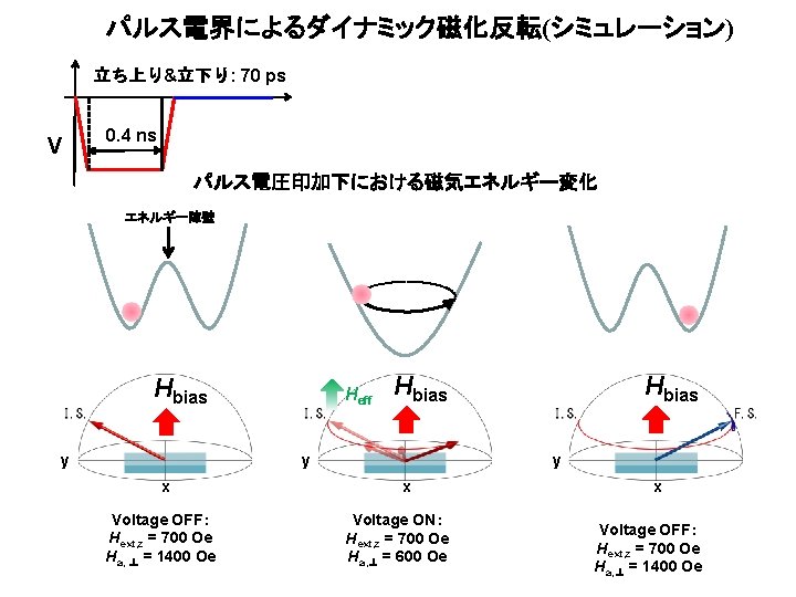
Macro-spin mode simulation z <LLG equation> x y Magnetic energy: 1600 1400 Hperp (Oe) From experiment; Ms = 1. 54 T Hc(0 K) = 25 Oe Hshift = 75 Oe Hperp (0 V) = 1400 Oe Hperp (-0. 75 V) = 600 Oe T = 300 K Parameter; a = 0. 01 1200 1000 800 600 400 -0. 75 -0. 25 0 0. 25 DC bias voltage (V)
Structure Slope (f. J/Vm) Ref. Au / Fe 80 Co 20 (0. 4 nm) / Mg. O -37 T. Nozaki et al. APL 2010 Ta / Co 40 Fe 40 B 20 (1. 33 nm) / Mg. O -33 M. Endo et al. APL 2010 Au / Fe 80 Co 20 (0. 7 nm) / Mg. O -31 Y. Shiota et al. APEX 2011 Au/Fe. Pt (1. 5 nm) /Mg. O 19 T. Seki et al. APL 2011 Ta / Co 60 Fe 20 B 20 (1. 2 nm) / Mg. O / Al 2 O 3 -11 K. Kita et al. JAP (2012) Ta / Co. Fe. B (1. 3 nm) / Mg. O -50 W. –G. Wang et al. Nat. Mater. (2012) Mg. O / Co. Fe. B (1. 8 nm) / Ta -33 S. Kanai et al. APL (2012) Ru / Co. Fe. B (1. 4 nm) / Mg. O 18 Y. Shiota et al. APL (2013) Mg. O / Fe. B (1. 5 nm) / Mg. O -108 T. Nozaki et al. APEX (2013) Mg. O / Fe(0. 3 nm) / Fe. B (1. 5 nm) / Ta -105 This study Vacuum / Fe (15 ML) / Vacuum -20 C. -G. Duan et al. PRL 2008 Vacuum / Fe (1 ML) / Vacuum -33 K. Nakamura et al. PRL 2009 Pt / Fe(1 ML) / Pt (1 ML) / Vacuum -72 M. Tsujikawa et al. PRL 2009 Cu / Fe (9 ML) / Mg. O 100 M. K. Niranjan et al. APL 2010 Au / Fe(2 ML) / Mg. O 11. 6 M. Tsujikawa et al. JAP 2012 Theory
Comparison of experimental results and simulation AP ⇒ P Experiment Vpulse = -0. 75 V Simulation P ⇒ AP
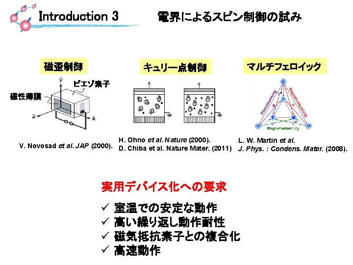
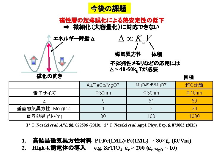
Introduction 5 垂直磁気異方性の起源 1. 3 d-白金族合金の結晶磁気異方性 L 10 -Fe(Co)Pt, Fe(Co)Pd 白金族系の強いスピン-軌道相互作用を活用 2. 界面誘起の垂直磁気異方性 Mg. O/3 d遷移金属界面 Fe/Mg. O ; T. Shinjo et al. J. de Physique 40, C 2 -86 -87 (1979). Co. Fe. B / Mg. O ; Ikeda et. al. Mature Mater. 9, 721 (2010). L 10 ordered Fe. Pt Ikeda et. al. Mature Mater. 9, 721 (2010) z 2 (m=0) Fe Mg O Mg. O 弱いFe dz 2 - O pz混成 ⇒ 垂直磁気異方性
Voltage-induced torque z x y
No influence from spin transfer torque? ? Discussion 1 Estimation of flowing tunneling current (current density) Too small! However…the ultrathin Fe. Co layer can be very sensitive to the current torques due to the very small HZ…
Spin transfer torque
Voltage-induced torque 103 times larger !
Comparison of the power consumption Spin torque induced FMR Cf. S. Ishibashi et al. Appl. Phys. Express, 3, 073001 (2010) Co. Fe. B / Mg. O / Co. Fe. B MTJ 100× 150 nm 2 RA: 2 Wmm 2, MR: 100% Precession angle: 1 deg. Consumed power: 1 m. W Voltage-field induced FMR Assuming the sample size… Precession angle : 1 deg. Consumed power: 0. 005 m. W Power reduction of 1/200!
Result 5 Input voltage dependence of the signal amplitude Tilted field angle: 55 deg. Hex = 500 Oe
Results 1 TMR curves Fe. Co thickness dependence (normalized MR curve) Difference in the saturation fields reflect the surface magnetic anisotropy
Bias voltage dependence of mag-noise spectrum Result 2 (t. Fe. Co: 0. 68 nm (Hperp=1500 Oe), t. Mg. O: 1. 5 nm, Hex = 2500 Oe) Kittel’s equation +V H -V Anisotropy change slope: 37 f. J/Vm Cf. Theory: Fe(1 ML) / Mg. O (3 ML) 29 f. J/Vm R. Shimabukuro et al. Physica E 42, 1014(2010)
Macro-spin model simulation Hex = 700 Oe Tilted angle: 84 degree
Estimation of precession angle, Dq
Second order perturbation theory (D. S. Wang et al. PRB, 47, 14932 (1993)) ko : k vector of occupied state ku : k vector of unoccupied state la (a= x, z): angular momentum operators. <o|lz|u> <o|lx|u> Out-of-plane In-plane x 2 -y 2(m=± 2) xy (m= 2) EF xz, yz (m=± 1) z 2 (m=0) xz, yz (m=± 1) xy (m= 2) Simplified band structure of the monolayer Fe
Electric field induced anisotropy change M. Tsujikawa and T. Oda, PRL 102, 247203 (2009). Pt Fe Pt
Ms = 1. 83× 106 A/m (Experiment) g= -2. 3× 10⁵ m/(A sec) (g=2. 1) a = 0. 01 (parameter) Hc(0 K) = 25 Oe (Experiment) Hshift = 73. 2 Oe ( Experiment ) Hs, perp (0 V/nm) = 1400 Oe ( Experiment ) Hs, perp (-1 V/nm) = 600 Oe ( Experiment )
Thickness dependence of the MS for Fe 80 Co 20 layer 1. 8 1. 44
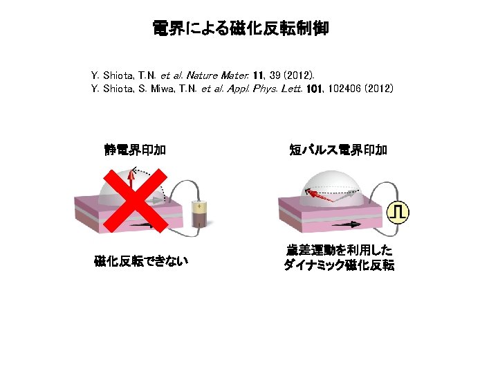
Dynamic switching 2 Voltage-induced magnetization switching of perpendicularly magnetized film J. Stöhr et al. Appl. Phys. Lett. 94, 072504 (2009)