INTRODUCING MICROWIND DEPARTMENT OF ELECTRICAL COMPUTER ENGINEERING WHAT

- Slides: 8

INTRODUCING MICROWIND DEPARTMENT OF ELECTRICAL & COMPUTER ENGINEERING

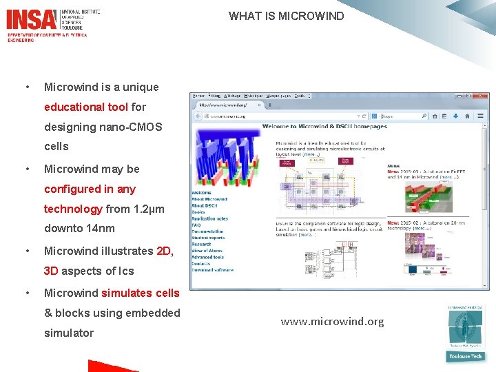
WHAT IS MICROWIND • Microwind is a unique educational tool for designing nano-CMOS cells • Microwind may be configured in any technology from 1. 2µm downto 14 nm • Microwind illustrates 2 D, 3 D aspects of Ics • Microwind simulates cells & blocks using embedded simulator www. microwind. org

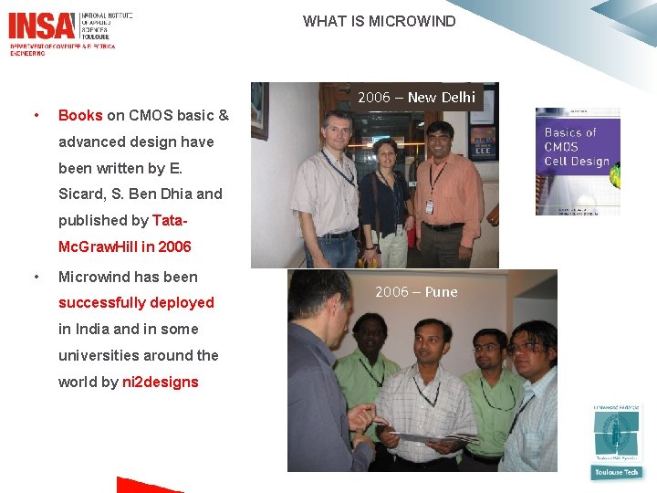
WHAT IS MICROWIND • 2006 – New Delhi Books on CMOS basic & advanced design have been written by E. Sicard, S. Ben Dhia and published by Tata. Mc. Graw. Hill in 2006 • Microwind has been successfully deployed 2006 – Pune in India and in some universities around the world by ni 2 designs www. microwind. org

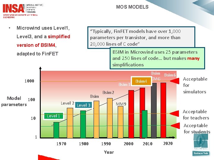
MOS MODELS • Microwind uses Level 1, “Typically, Fin. FET models have over 1, 000 parameters per transistor, and more than 20, 000 lines of C code” BSIM in Microwind uses 25 parameters and 250 lines of code… but makes many simplifications Level 3, and a simplified version of BSIM 4, adapted to Fin. FET 1000 Bsim 3 Bsim Model 100 parameters Bsim 2 Level 3 10 Bsim 6 Bsim 4 CMG MM 9 Acceptable for teachers Acceptable for students Level 1 1 1970 Acceptable for simulators 1980 1990 Year 2000 2010 2020

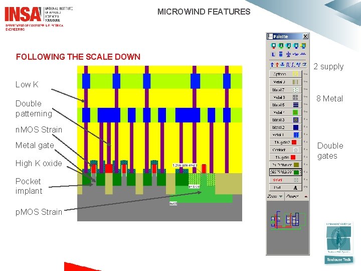
MICROWIND FEATURES FOLLOWING THE SCALE DOWN 2 supply Low K Double patterning 8 Metal n. MOS Strain Metal gate High K oxide Pocket implant p. MOS Strain Double gates

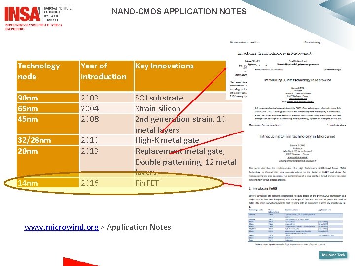
NANO-CMOS APPLICATION NOTES Technology node Year of Key Innovations introduction 90 nm 65 nm 45 nm 2003 2004 2008 32/28 nm 2010 2013 14 nm 2016 SOI substrate Strain silicon 2 nd generation strain, 10 metal layers High-K metal gate Replacement metal gate, Double patterning, 12 metal layers Fin. FET www. microwind. org > Application Notes

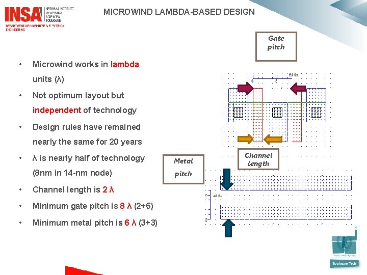
MICROWIND LAMBDA-BASED DESIGN Gate pitch • Microwind works in lambda units (λ) • Not optimum layout but independent of technology • Design rules have remained nearly the same for 20 years • λ is nearly half of technology Metal (8 nm in 14 -nm node) pitch • Channel length is 2 λ • Minimum gate pitch is 8 λ (2+6) • Minimum metal pitch is 6 λ (3+3) Channel length

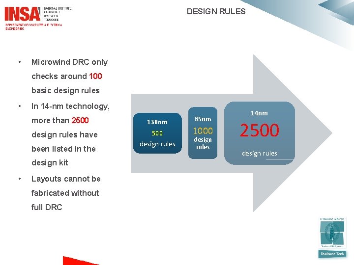
DESIGN RULES • Microwind DRC only checks around 100 basic design rules • In 14 -nm technology, more than 2500 design rules have been listed in the design kit • Layouts cannot be fabricated without full DRC 130 nm 500 design rules 65 nm 1000 design rules 14 nm 2500 design rules