Interpreting the Timing Diagram The 68000 Read Cycle
- Slides: 32

Interpreting the Timing Diagram The 68000 Read Cycle 3/11/2021 1

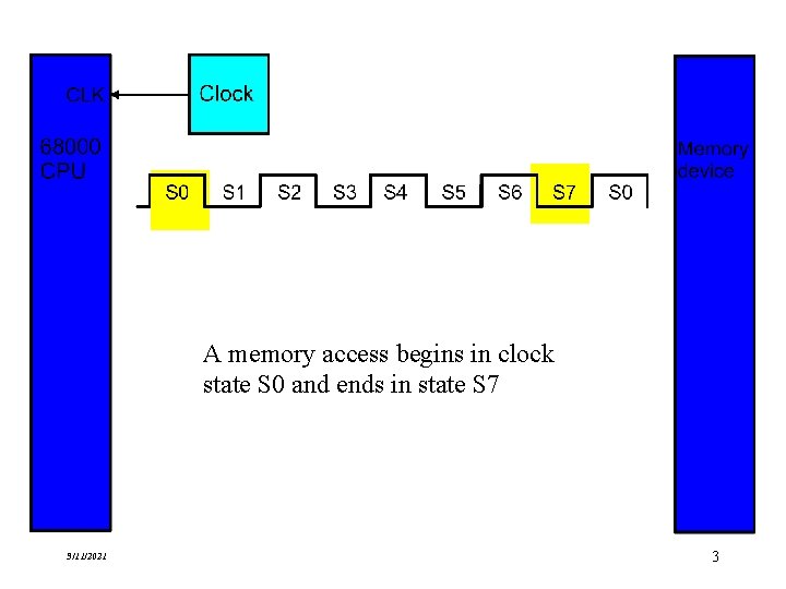
The Clock • A microprocessor requires a clock that provides a stream of timing pulses to control its internal operations • A 68000 memory access takes a minimum of eight clock states numbered from clock state S 0 to clock state S 7 3/11/2021 2

A memory access begins in clock state S 0 and ends in state S 7 3/11/2021 3

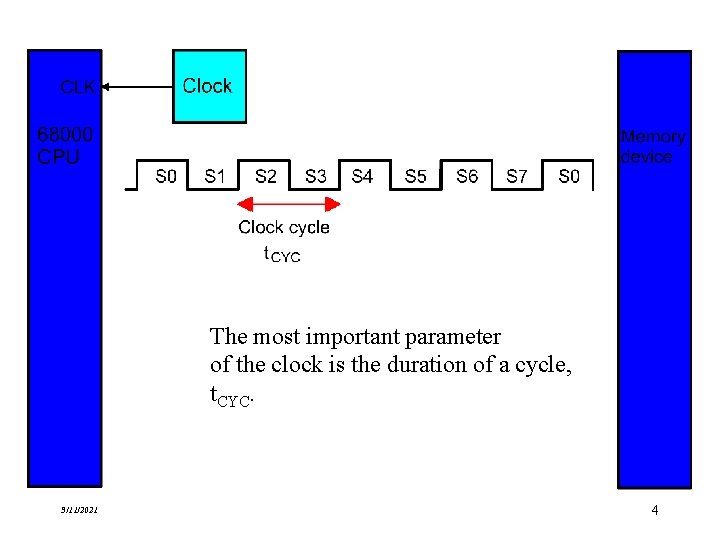
The most important parameter of the clock is the duration of a cycle, t. CYC. 3/11/2021 4

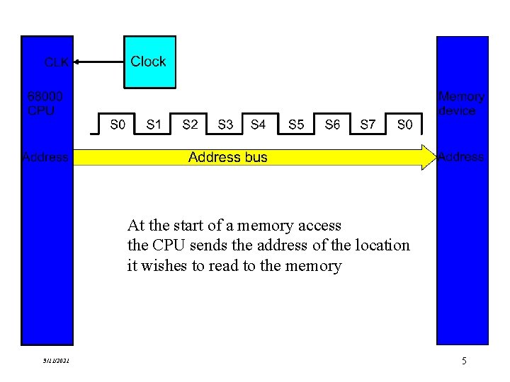
At the start of a memory access the CPU sends the address of the location it wishes to read to the memory 3/11/2021 5

Address Timing • We are interested in when the 68000 generates a new address for use in the current memory access • The next slide shows the relationship between the new address and the state of the 68000’s clock 3/11/2021 6

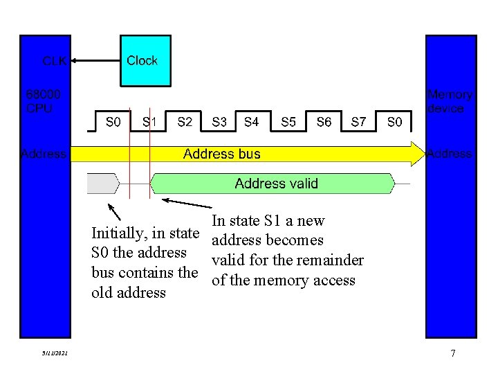
In state S 1 a new Initially, in state address becomes S 0 the address valid for the remainder bus contains the of the memory access old address 3/11/2021 7

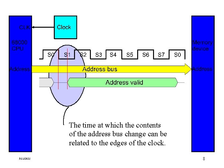
The time at which the contents of the address bus change can be related to the edges of the clock. 3/11/2021 8

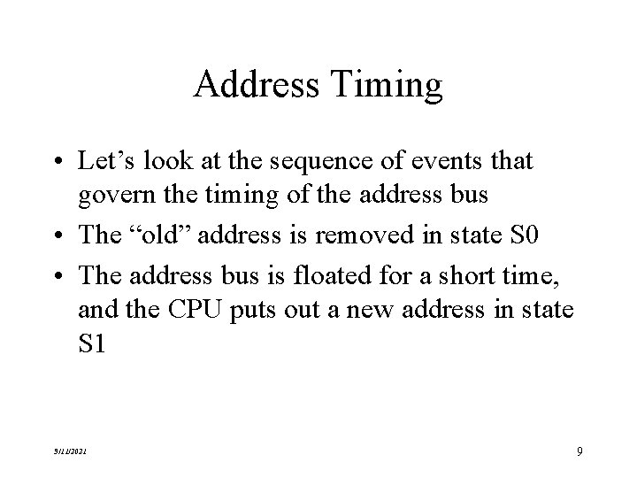
Address Timing • Let’s look at the sequence of events that govern the timing of the address bus • The “old” address is removed in state S 0 • The address bus is floated for a short time, and the CPU puts out a new address in state S 1 3/11/2021 9

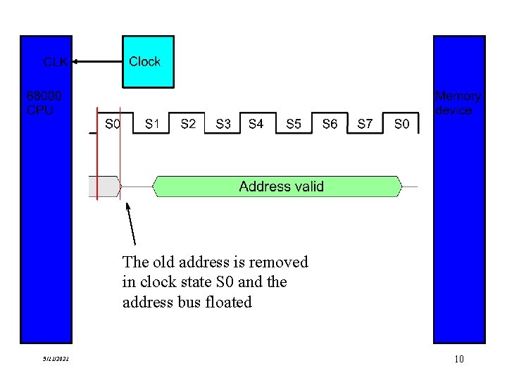
The old address is removed in clock state S 0 and the address bus floated 3/11/2021 10

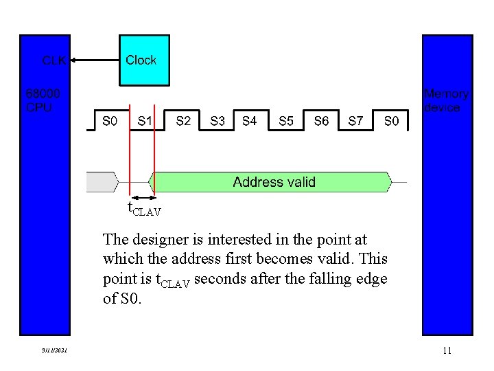
t. CLAV The designer is interested in the point at which the address first becomes valid. This point is t. CLAV seconds after the falling edge of S 0. 3/11/2021 11

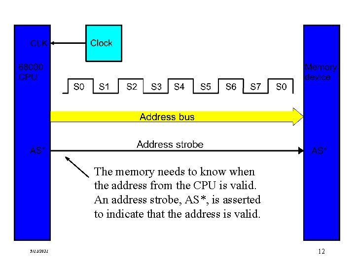
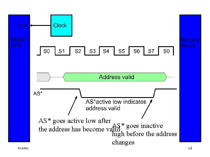
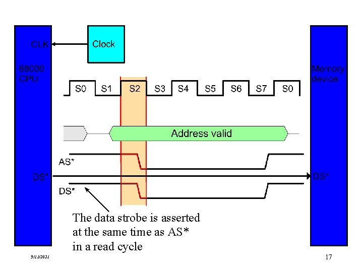
The memory needs to know when the address from the CPU is valid. An address strobe, AS*, is asserted to indicate that the address is valid. 3/11/2021 12

Address and Address Strobe • We are interested in the relationship between the time at which the address is valid and the time at which the address strobe, AS*, is asserted • When AS* is active-low it indicates that the address is valid • We now look at the timing of the clock, the address, and the address strobe 3/11/2021 13

AS* goes active low after AS* goes inactive the address has become valid high before the address changes 3/11/2021 14

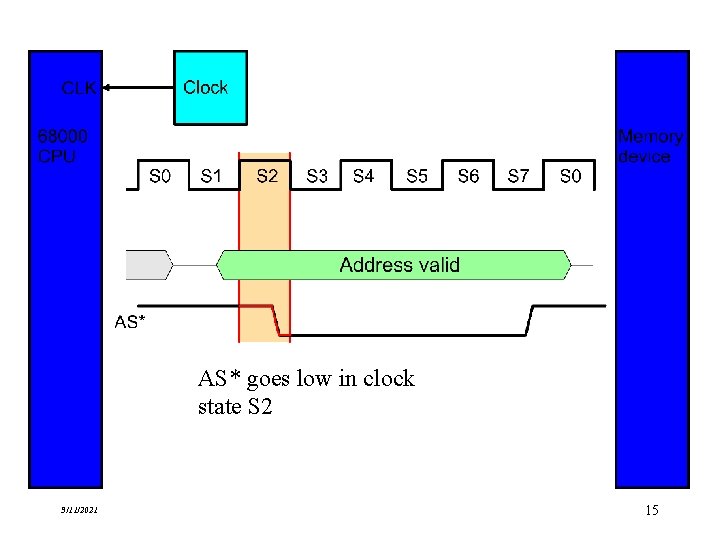
AS* goes low in clock state S 2 3/11/2021 15

The Data Strobes • The 68000 has two data strobes LDS* and UDS*. These select the lower byte or the upper byte of a word during a memory access • To keep things simple, we will use a single data strobe, DS* • The timing of DS* in a read cycle is the same as the address strobe, AS* 3/11/2021 16

The data strobe is asserted at the same time as AS* in a read cycle 3/11/2021 17

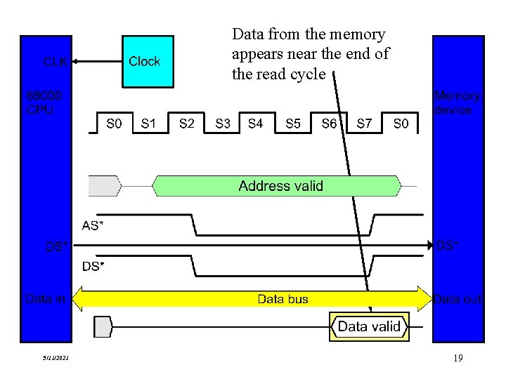
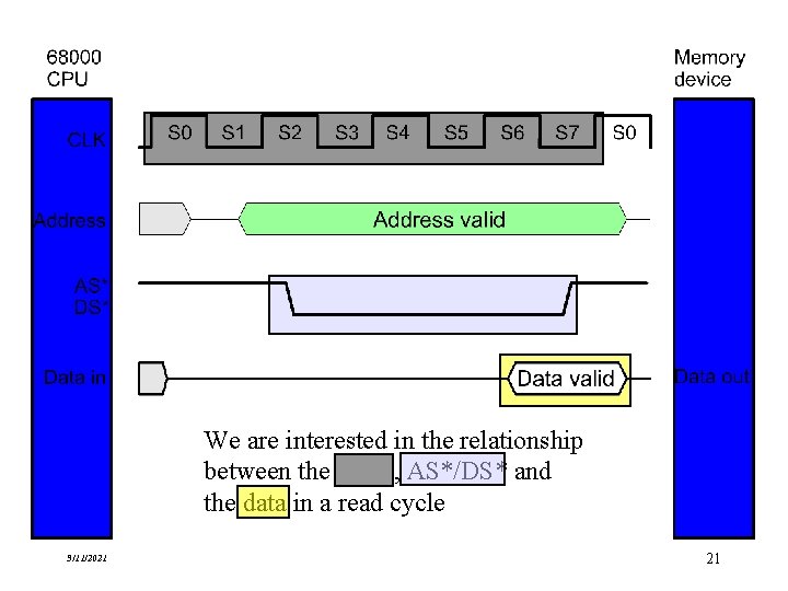
The Data Bus • During a read cycle the memory provides the CPU with data • The next slide shows the data bus and the timing of the data signal • Note that valid data does not appear on the data bus until near the end of the read cycle 3/11/2021 18

Data from the memory appears near the end of the read cycle 3/11/2021 19

Analyzing the Timing Diagram • We are going to redraw the timing diagram to remove clutter • We aren’t interested in the signal paths themselves, only in the relationship between the signals 3/11/2021 20

We are interested in the relationship between the clock, AS*/DS* and the data in a read cycle 3/11/2021 21

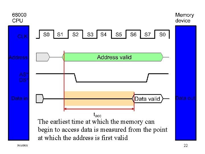
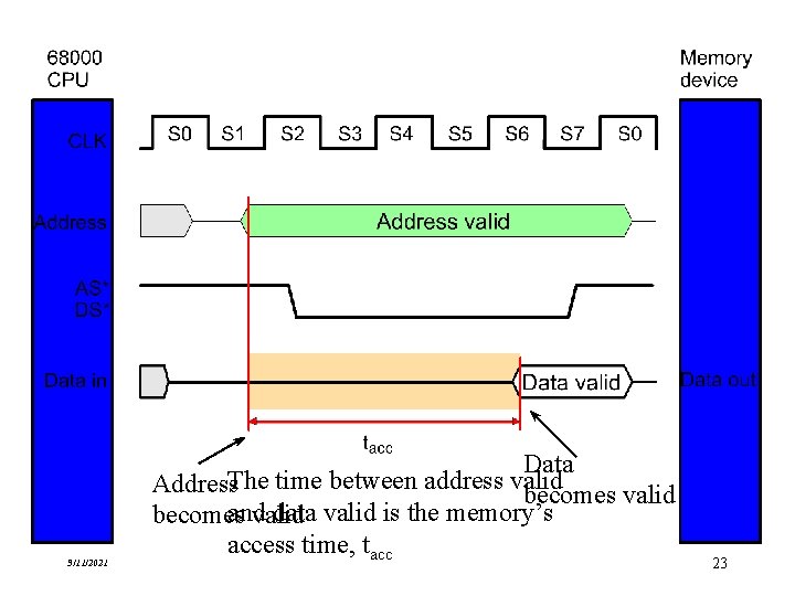
The earliest time at which the memory can begin to access data is measured from the point at which the address is first valid 3/11/2021 22

3/11/2021 Data Address. The time between address valid becomes valid and data valid is the memory’s becomes valid access time, tacc 23

Calculating the Access Time • We need to calculate the memory’s access time • By knowing the access time, we can use the appropriate memory component • Equally, if we select a given memory component, we can calculate whether its access time is adequate for a particular system 3/11/2021 24

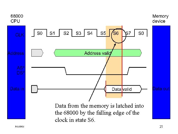
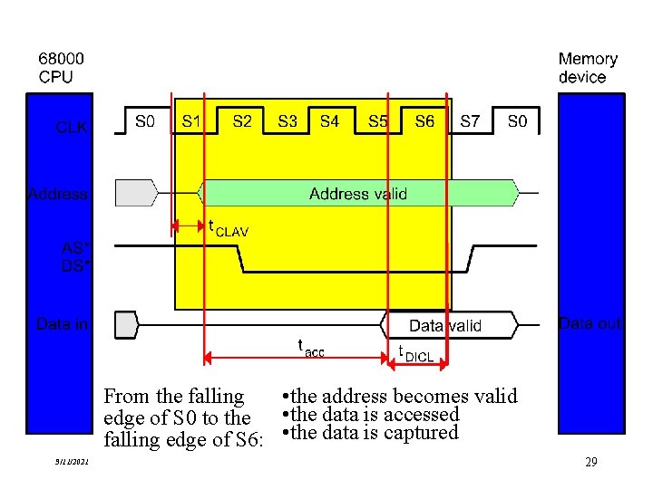
Data from the memory is latched into the 68000 by the falling edge of the clock in state S 6. 3/11/2021 25

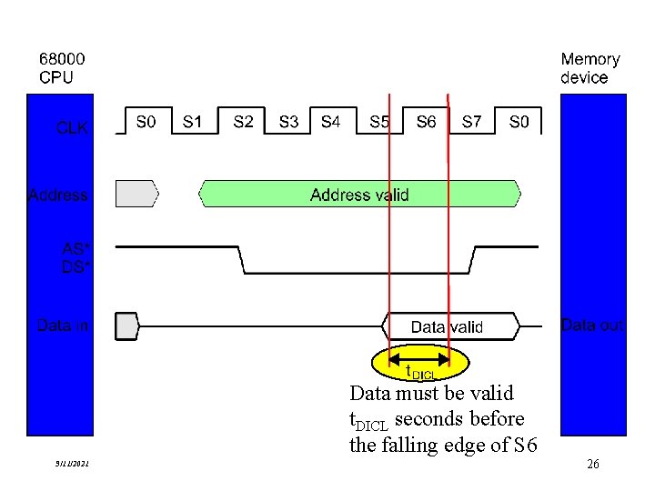
Data must be valid t. DICL seconds before the falling edge of S 6 3/11/2021 26

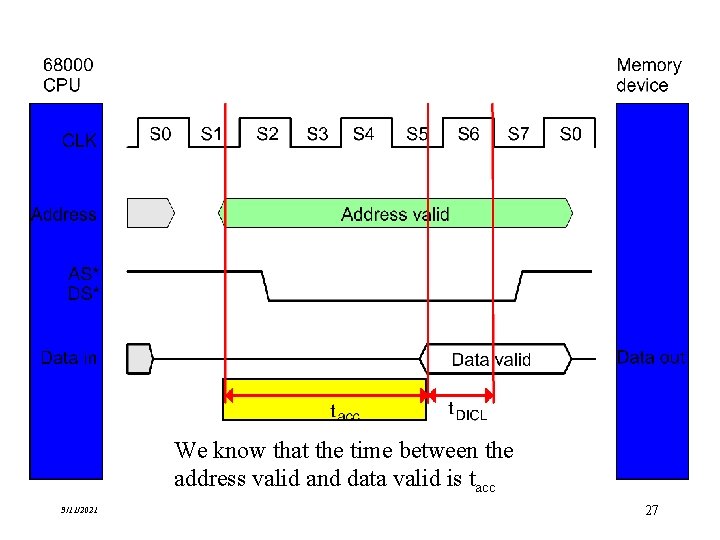
We know that the time between the address valid and data valid is tacc 3/11/2021 27

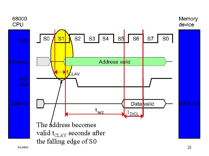
The address becomes valid t. CLAV seconds after the falling edge of S 0 3/11/2021 28

From the falling • the address becomes valid edge of S 0 to the • the data is accessed falling edge of S 6: • the data is captured 3/11/2021 29

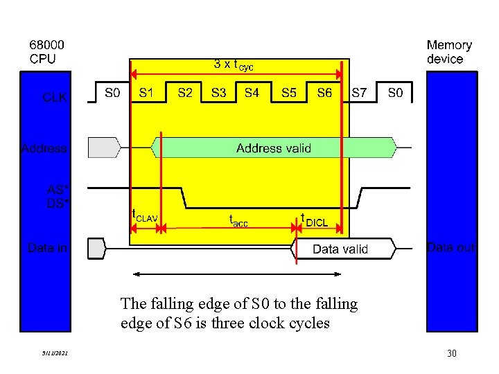
The falling edge of S 0 to the falling edge of S 6 is three clock cycles 3/11/2021 30

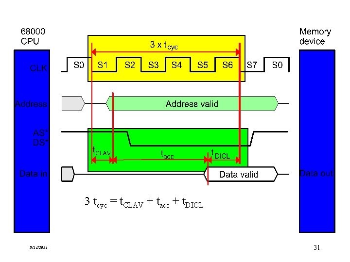
3 tcyc = t. CLAV + tacc + t. DICL 3/11/2021 31

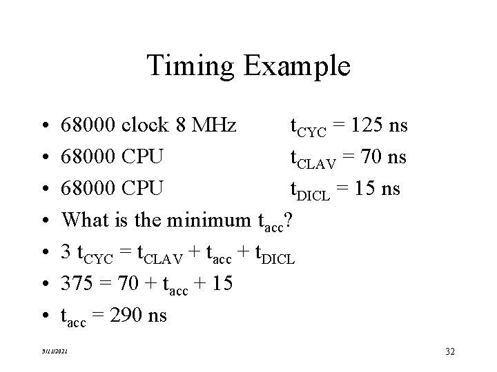
Timing Example • • 68000 clock 8 MHz t. CYC = 125 ns 68000 CPU t. CLAV = 70 ns 68000 CPU t. DICL = 15 ns What is the minimum tacc? 3 t. CYC = t. CLAV + tacc + t. DICL 375 = 70 + tacc + 15 tacc = 290 ns 3/11/2021 32