Interlock System DCS Training Session 2 3 Joachim
- Slides: 12

Interlock System DCS Training Session 2. 3 Joachim Schultes University of Wuppertal

Overview Interlock System • Structure • Numbers Components • BBIM (Temperature Interlock, see session 1) • PP 1 Box (Laser Interlock) • BOC-I-Box (Laser Interlock) • Logic Units • Interlock Distribution Box Joachim Schultes DCS Training 2007: Interlock System

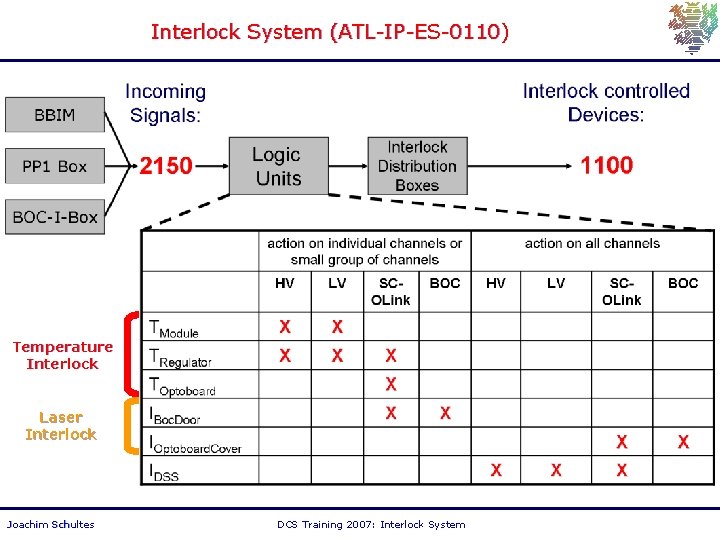
Interlock System (ATL-IP-ES-0110) Temperature Interlock Laser Interlock Joachim Schultes DCS Training 2007: Interlock System

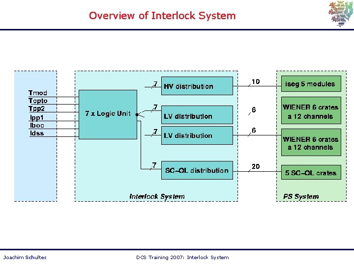
Overview of Interlock System Joachim Schultes DCS Training 2007: Interlock System

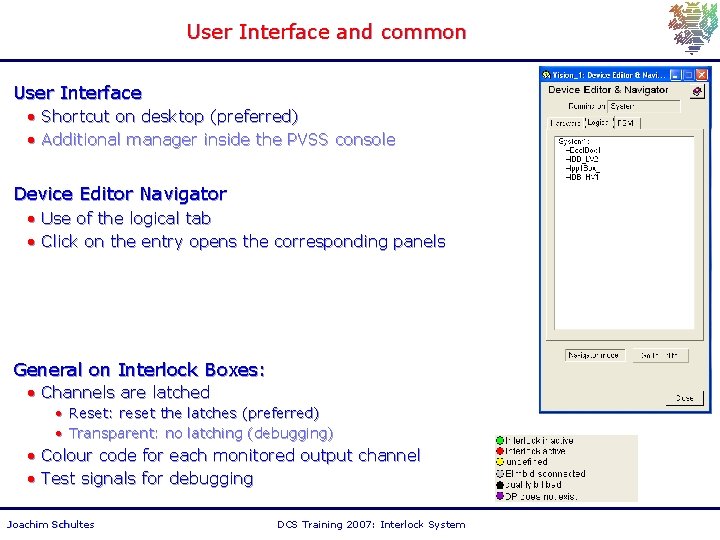
User Interface and common User Interface • Shortcut on desktop (preferred) • Additional manager inside the PVSS console Device Editor Navigator • Use of the logical tab • Click on the entry opens the corresponding panels General on Interlock Boxes: • Channels are latched • Reset: reset the latches (preferred) • Transparent: no latching (debugging) • Colour code for each monitored output channel • Test signals for debugging Joachim Schultes DCS Training 2007: Interlock System

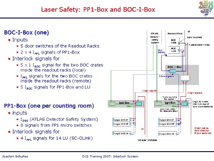
Laser Safety: PP 1 -Box and BOC-I-Box (one) • Inputs • 5 door switches of the Readout Racks • 2 x 4 IPP 1 signals of PP 1 -Box • Interlock signals for • 5 x 1 IBOC signal for the two BOC crates inside the readout racks (local) • IPP 1 signals for the two BOC crates inside the readout racks (remote) • 5 IBOC signals for PP 1 -Box and LU PP 1 -Box (one per counting room) • inputs • IDSS (ATLAS Detector Safety System) • 8 signals from PP 1 micro switches • Interlock signals for • 4 IPP 1 signals for 14 LU (SC-OLink) Joachim Schultes DCS Training 2007: Interlock System

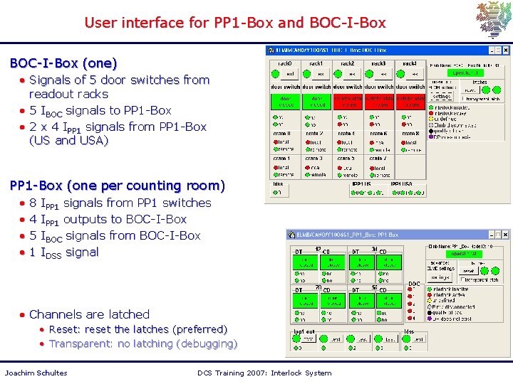
User interface for PP 1 -Box and BOC-I-Box (one) • Signals of 5 door switches from readout racks • 5 IBOC signals to PP 1 -Box • 2 x 4 IPP 1 signals from PP 1 -Box (US and USA) PP 1 -Box (one per counting room) • 8 IPP 1 signals from PP 1 switches • 4 IPP 1 outputs to BOC-I-Box • 5 IBOC signals from BOC-I-Box • 1 IDSS signal • Channels are latched • Reset: reset the latches (preferred) • Transparent: no latching (debugging) Joachim Schultes DCS Training 2007: Interlock System

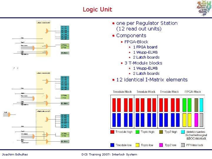
Logic Unit • one per Regulator Station (12 read out units) • Components • FPGA-Block • 1 FPGA board • 1 Wupp-ELMB • 2 Latch boards • 3 T-Module blocks • 1 Wupp-ELMB • 2 Latch boards • 12 identical I-Matrix elements Joachim Schultes DCS Training 2007: Interlock System

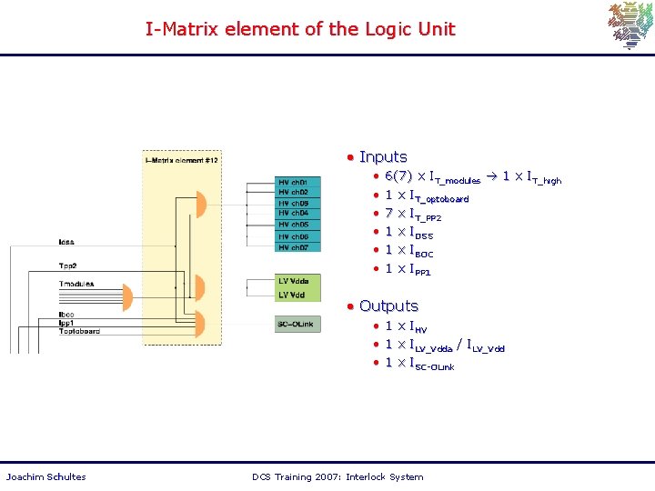
I-Matrix element of the Logic Unit • Inputs • • • 6(7) x IT_modules 1 x IT_high 1 x IT_optoboard 7 x IT_PP 2 1 x IDSS 1 x IBOC 1 x IPP 1 • Outputs • 1 x IHV • 1 x ILV_Vdda / ILV_Vdd • 1 x ISC-OLink Joachim Schultes DCS Training 2007: Interlock System

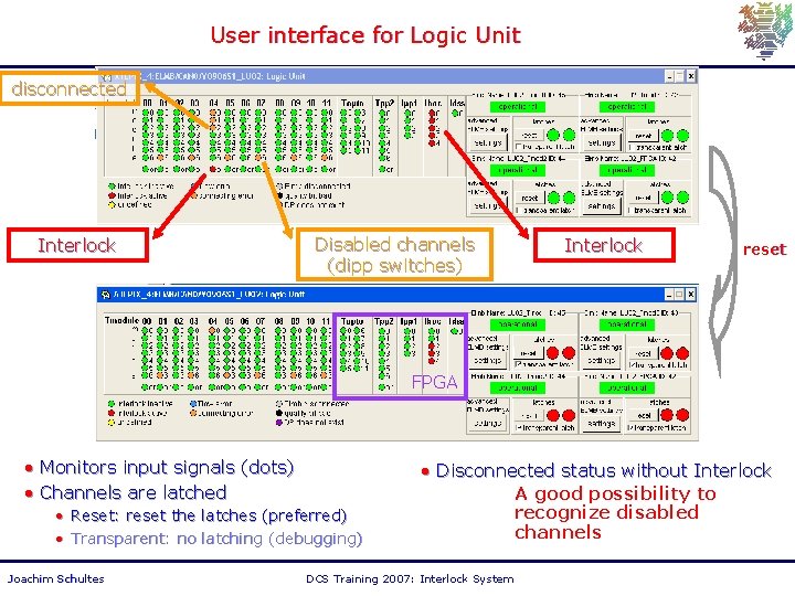
User interface for Logic Unit disconnected Interlock Disabled channels (dipp switches) Interlock reset FPGA • Monitors input signals (dots) • Channels are latched • Reset: reset the latches (preferred) • Transparent: no latching (debugging) Joachim Schultes • Disconnected status without Interlock A good possibility to recognize disabled channels DCS Training 2007: Interlock System

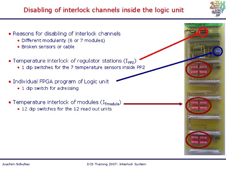
Disabling of interlock channels inside the logic unit • Reasons for disabling of interlock channels • Different modularity (6 or 7 modules) • Broken sensors or cable • Temperature interlock of regulator stations (IPP 2) • 1 dip switches for the 7 temperature sensors inside PP 2 • Individual FPGA program of Logic unit • 1 dip switch for adressing • Temperature interlock of modules (ITmodule) • 12 dip switches for the 12 read out units Joachim Schultes DCS Training 2007: Interlock System

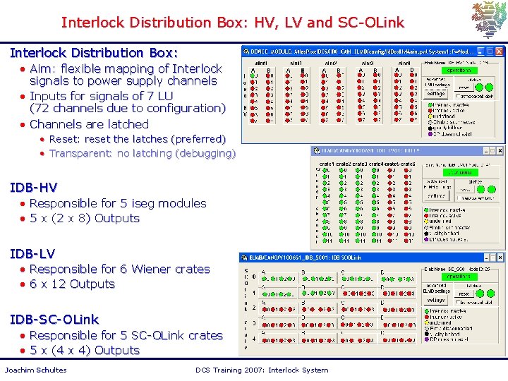
Interlock Distribution Box: HV, LV and SC-OLink Interlock Distribution Box: • Aim: flexible mapping of Interlock signals to power supply channels • Inputs for signals of 7 LU (72 channels due to configuration) • Channels are latched • Reset: reset the latches (preferred) • Transparent: no latching (debugging) IDB-HV • Responsible for 5 iseg modules • 5 x (2 x 8) Outputs IDB-LV • Responsible for 6 Wiener crates • 6 x 12 Outputs IDB-SC-OLink • Responsible for 5 SC-OLink crates • 5 x (4 x 4) Outputs Joachim Schultes DCS Training 2007: Interlock System