Interfacing External Memory Rajiv Nandivada High Level Schematic
- Slides: 16

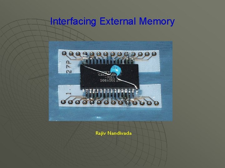
Interfacing External Memory Rajiv Nandivada

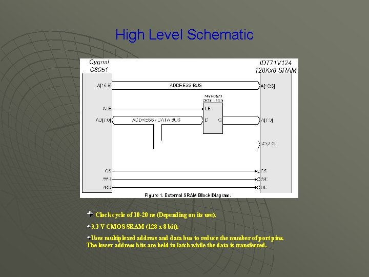
High Level Schematic Clock cycle of 10 -20 ns (Depending on its use). 3. 3 V CMOS SRAM (128 x 8 bit). Uses multiplexed address and data bus to reduce the number of port pins. The lower address bits are held in latch while the data is transferred.

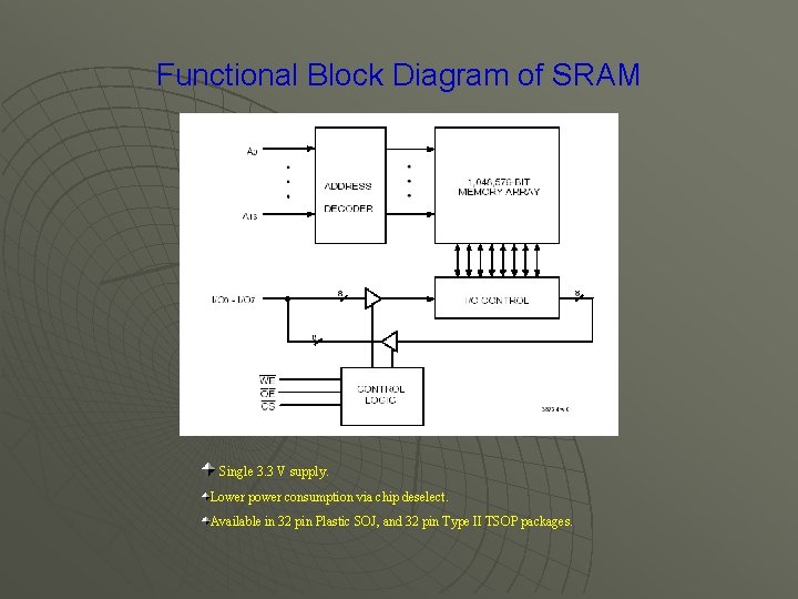
Functional Block Diagram of SRAM Single 3. 3 V supply. Lower power consumption via chip deselect. Available in 32 pin Plastic SOJ, and 32 pin Type II TSOP packages.

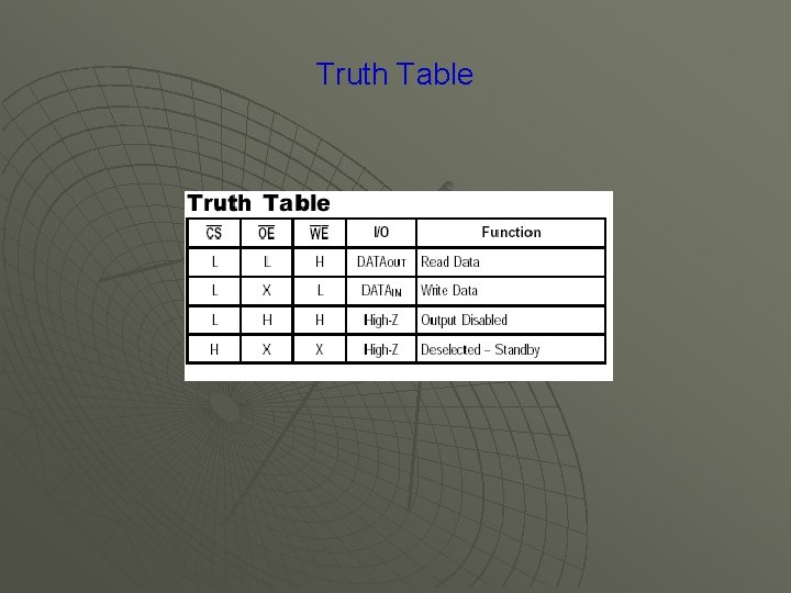
Truth Table

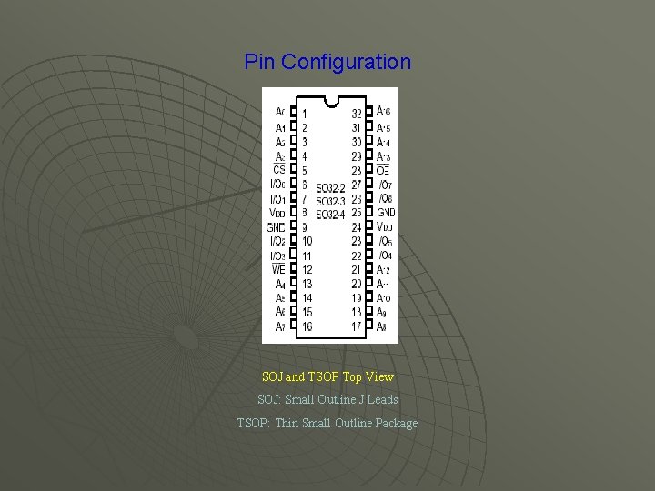
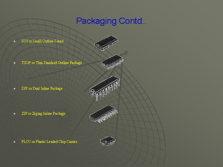
Pin Configuration SOJ and TSOP Top View SOJ: Small Outline J Leads TSOP: Thin Small Outline Package

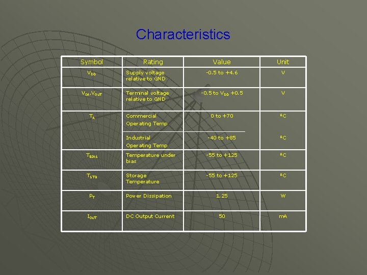
Characteristics Symbol VDD Rating Supply voltage relative to GND Value Unit -0. 5 to +4. 6 V VIN, VOUT Terminal voltage relative to GND -0. 5 to VDD +0. 5 V TA Commercial Operating Temp 0 to +70 0 C Industrial Operating Temp -40 to +85 0 C TBIAS Temperature under bias -55 to +125 0 C TSTG Storage Temperature -55 to +125 0 C PT Power Dissipation 1. 25 W IOUT DC Output Current 50 m. A

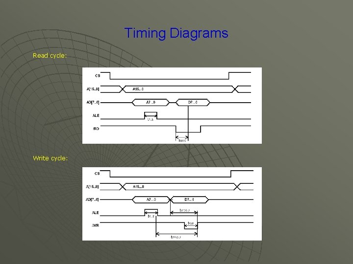
Timing Diagrams Read cycle: Write cycle:

Major Manufacturers of SRAM • • • • • Alliance, Brilliance Crosslink Cypress Semiconductor Dense-PAC Micro Etron Technology Eureka Hitachi IBM IDT Mitsubishi NEC Samsung Seiko Epson Sharp Sony Toshiba

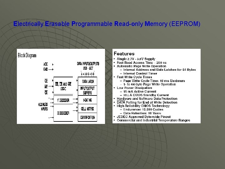
Electrically Erasable Programmable Read-only Memory (EEPROM)

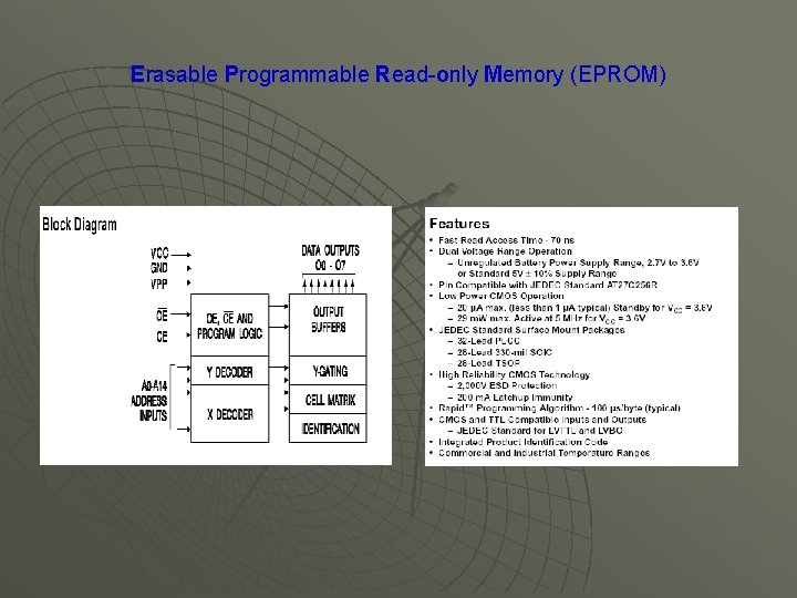
Erasable Programmable Read-only Memory (EPROM)

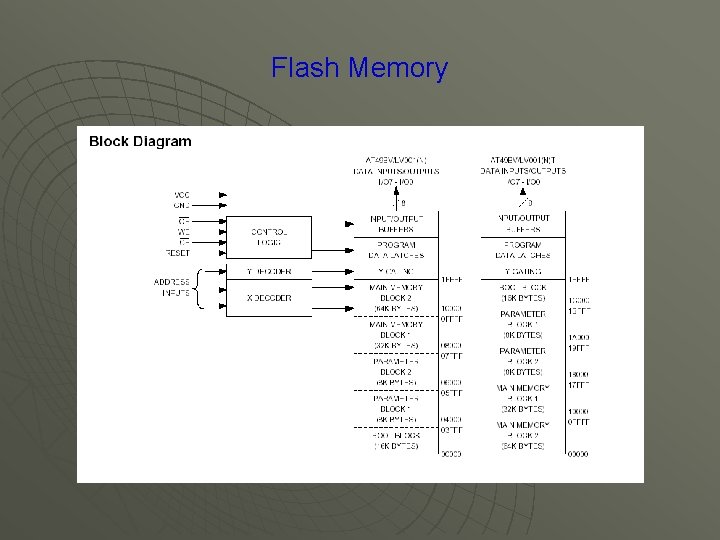
Flash Memory

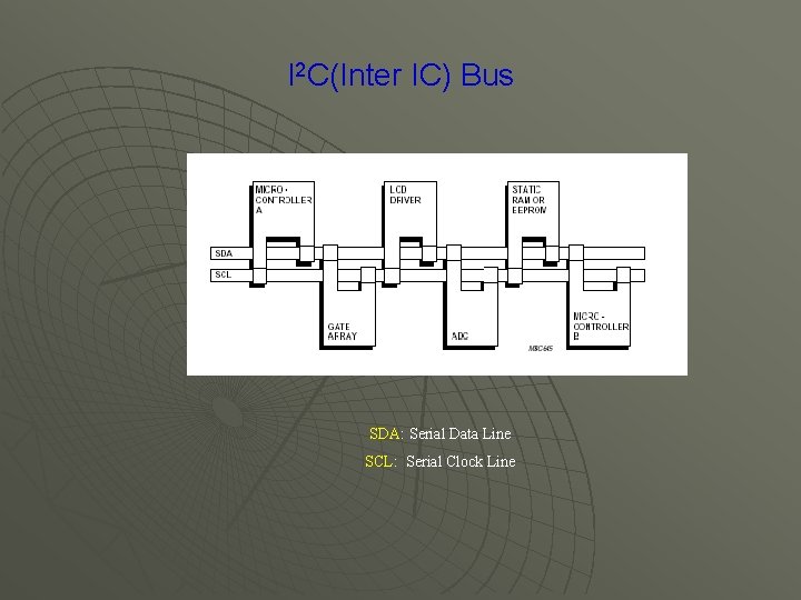
I 2 C(Inter IC) Bus SDA: Serial Data Line SCL: Serial Clock Line

Packaging u u • SOJ or Small Outline J-lead TSOP or Thin Standard Outline Package DIP or Dual Inline Package ZIP or Zigzag Inline Package PLCC or Plastic Leaded Chip Carrier

Packaging Contd. . u SOJ or Small Outline J-lead u TSOP or Thin Standard Outline Package u DIP or Dual Inline Package u ZIP or Zigzag Inline Package u PLCC or Plastic Leaded Chip Carrier

Pricing Depends on • • • The type of package it comes in (DIP, SOJ, TSOP) The speed of the memory. The market value. The vendor (Digikey, Jameco) Storage capacity( 128 K X 8, 256 K X 8) The type of memory (Flash, EEPROM)

References • • • www. cygnal. com www. digikey. com www. srams. co. uk www. jameco. com www. atmel. com www. xicor. com