
Interconnect Routing in VLSI Glauco Borges Valim dos
Interconnect Routing in VLSI Glauco Borges Valim dos Santos - FUCAS - GME - II - UFRGS - 2004
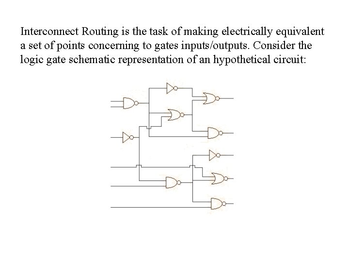
Interconnect Routing is the task of making electrically equivalent a set of points concerning to gates inputs/outputs. Consider the logic gate schematic representation of an hypothetical circuit:
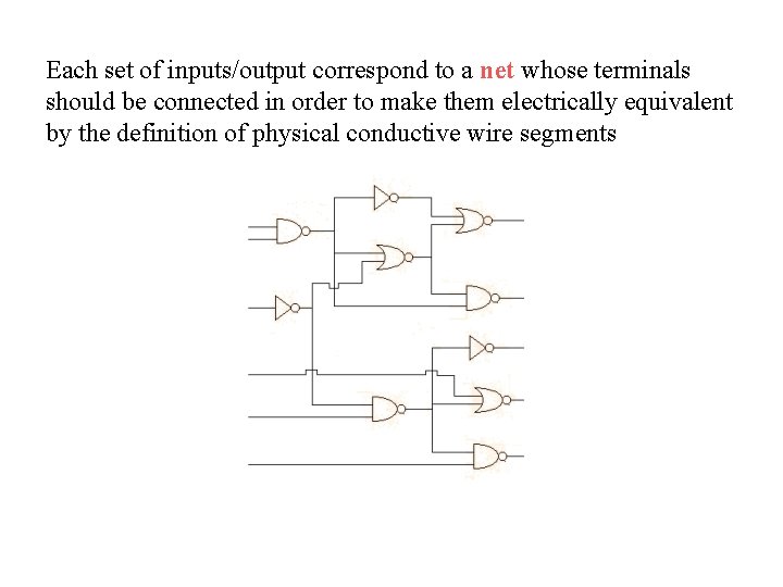
Each set of inputs/output correspond to a net whose terminals should be connected in order to make them electrically equivalent by the definition of physical conductive wire segments
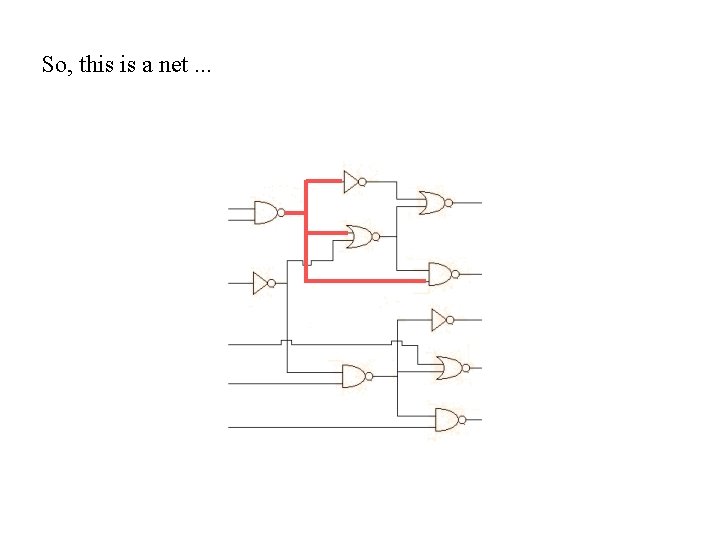
So, this is a net. . .
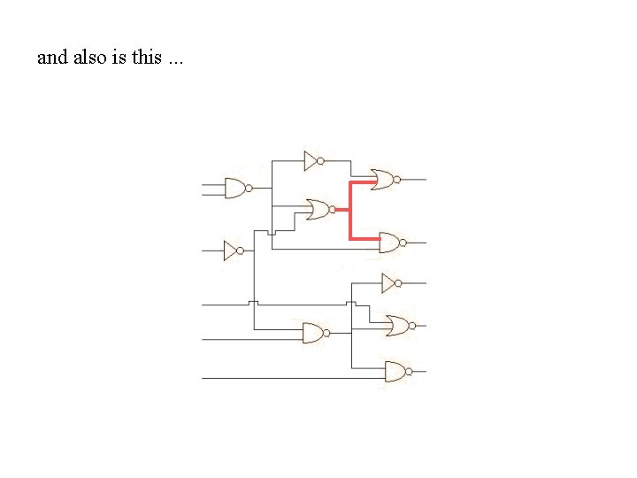
and also is this. . .
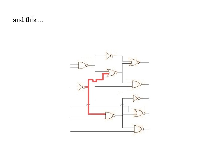
and this. . .
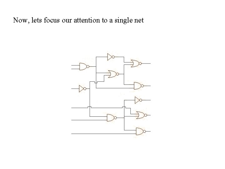
Now, lets focus our attention to a single net
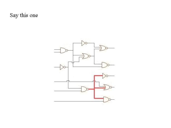
Say this one
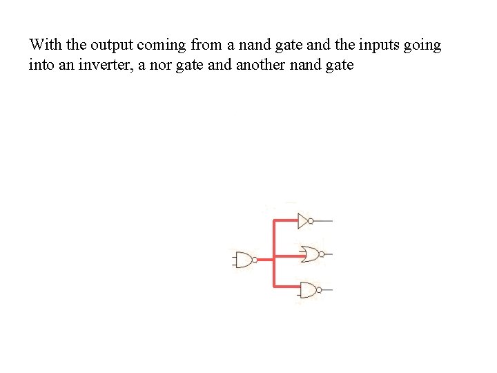
With the output coming from a nand gate and the inputs going into an inverter, a nor gate and another nand gate
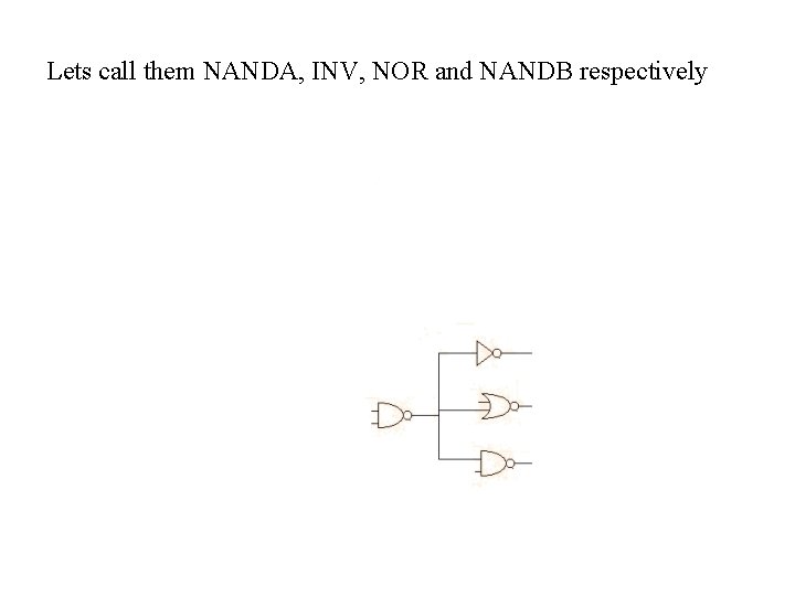
Lets call them NANDA, INV, NOR and NANDB respectively
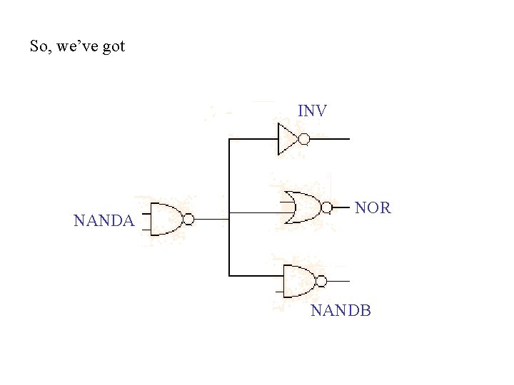
So, we’ve got INV NANDA NOR NANDB
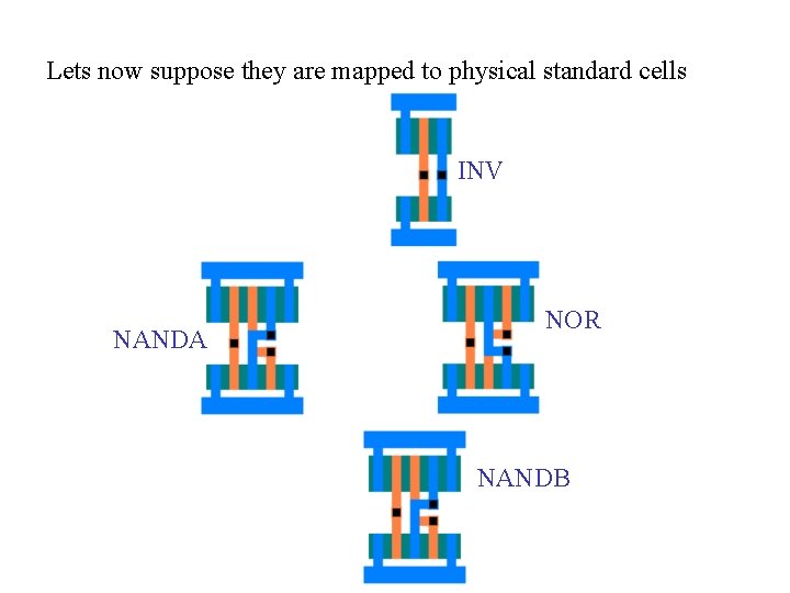
Lets now suppose they are mapped to physical standard cells INV NANDA NOR NANDB
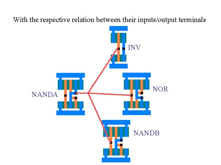
With the respective relation between their inputs/output terminals INV NANDA NOR NANDB
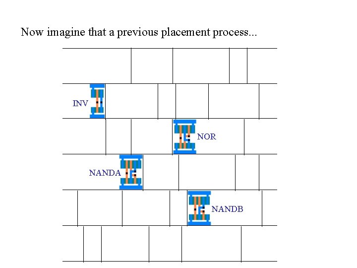
Now imagine that a previous placement process. . . INV NOR NANDA NANDB
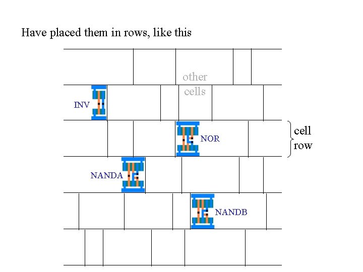
Have placed them in rows, like this other cells INV NOR NANDA NANDB cell row
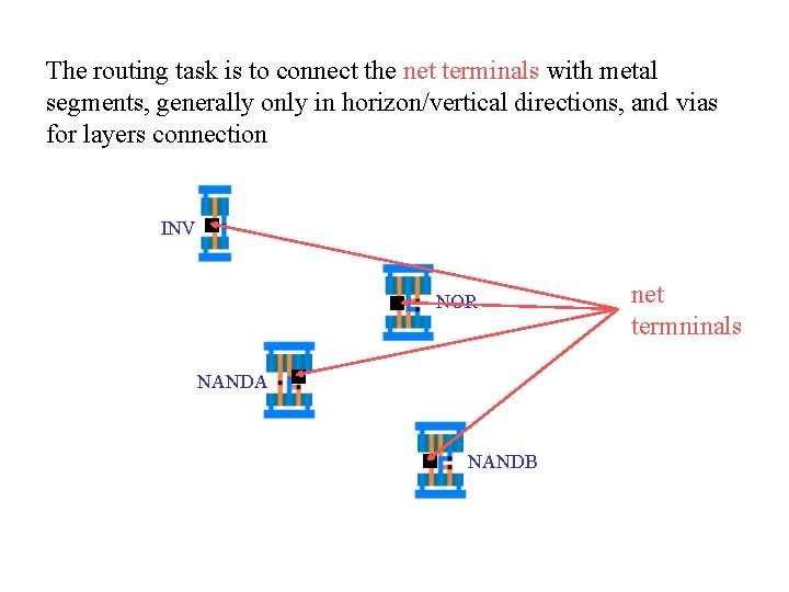
The routing task is to connect the net terminals with metal segments, generally only in horizon/vertical directions, and vias for layers connection INV NOR NANDA NANDB net termninals
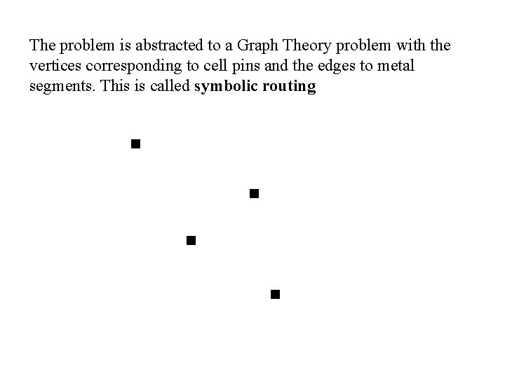
The problem is abstracted to a Graph Theory problem with the vertices corresponding to cell pins and the edges to metal segments. This is called symbolic routing
- Slides: 17