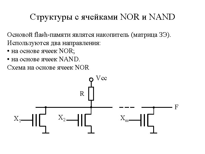
Intel Processors Processor name Year Number of transistors


Intel Processors Processor name Year Number of transistors 4004 1971 2 300 8008 1972 2 500 8080 1974 5 000 8086 1978 29 000 286 1982 120 000 Intel 386 1985 275 000 Intel 486 1989 1 180 000 Intel Pentium 1993 3 100 000 Pentium Pro 1995 5 500 000 Intel Pentium II 1997 7 500 000 Intel Pentium III 1999 24 000 -28 000 Intel Pentium 4 2000 42 000 Intel Itanium 2002 220 000 Intel Itanium 2 2003 410 000
 Intel, HP 2")
Processors Processor name Cores Year Number of transistors Intel Itanium (Montecito) Intel, HP 2 2006 1 720 000 Intel Core 2 Duo (Conroe) Intel 2 2006 291 000 Tukwila Intel, HP 4(65 nm) 2009 2 000 000 Open SPARC T 1 Open SPARC T 2 Sun 8 4 8 8 2005 2007 300 000 Phenom X 3 8750 AMD 3 4(65 nm) Intel 2 (45 nm) Intel 4 2008 Intel 6 2008 Phenom X 4 9550 Core 2 Duo E 8500 Core 2 Extreme QX 9770 Xeon X 7460 1 900 000

Intel Processors Processor Name Cores/ Threads Tech. process nm GHz L 2, L 1 Cache Size L 3 Cache MB Power W Year Xeon X 5560 4/8 45 2, 8/3, 2 4 256 K L 1 32 K/32 K 8 95 2008 Core 2 Quad Q 9650 4/4 45 3, 0 2 6 M L 1 32 K/32 K - 95 2008 4/4 45 3, 4 4 512 L 1 64/64 6 M 140 2008 Phenom

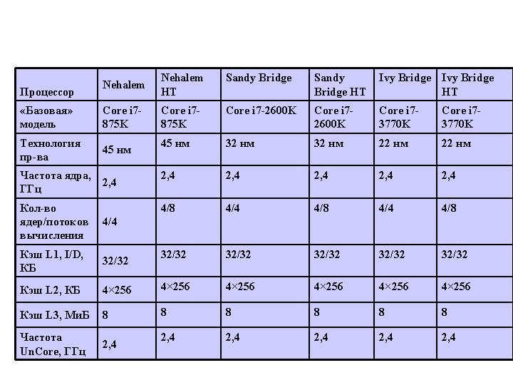
Intel Processors Nehalem Cores/ Threads Tech. Process nm 4/8 Core i 7940 Core i 7920 Core i 7 L 3 Cache size MB Power W Year GHz L 2 Cache Size KB 45 3, 2 4 256 8 130 2008, november 4/8 45 2, 93 4 256 8 130 2008, november 4/8 45 2, 65 4 256 8 130 2008, november Exstreme Edition L 1 32 K/32 K. Difference from Core 2 Duo : hyper-threading, L 3 Cache Производительность растет от поколения к поколению
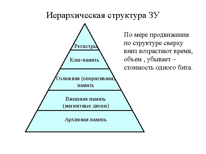

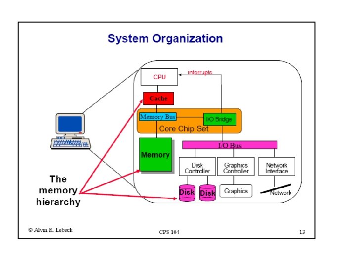
Иерархия памяти Registers L 1 ICache L 1 DCache L 2 Cache L 3 Cache Main Memory Disk (Swap) CPU is small part of system, most of system is memory hierarchy

Memory Hierarchy levels can be grouped in different ways: • by ISA visibility • registers • caches, memory, disk (swap): look like one thing • disk (file system) • by implementation technology • registers, cache: SRAM (high speed circuits) • main memory: DRAM (high density technology) • disk: magnetic iron oxide (electrical/mechanical)

Type Capacity Technology Latency Bandwith Registers <1 KB Custom memory with multiple ports, CMOS 1 ns 150 GB/s L 1 Cache <256 KB On-chip CMOS SRAM 4 ns 50 GB/s L 2 Cache <16 MB On-chip CMOS SRAM 10 ns 25 GB/s L 3 Cache 8 MB, … On-chip or off 30 MB chip CMOS SRAM 20 ns 10 GB/s Memory <16 GB CMOS DRAM 50 ns 4 GB/s Disk Storage < 3 ТB Magnetic disk 2, 5 -16 ms 44 -300 MB/s 3 TB Magnetic disk 3 – 12, 5 ms Seagate Barracuda 7200. 11 Momentus 5400. 3

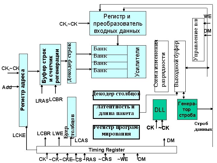
DDR RAM Частота шины Теоретическая способность GB/s 1 -канальный режим пропускная 2 -канальный DDR 3 -800 400 M Hz 6. 4 12, 8 DDR 3 -1066 533 M Hz 8, 53 17, 07 DDR 3 -1333 667 M Hz 10, 67 21, 33 DDR 3 -1600 800 M Hz 12, 8 25, 6 DDR 3 -1866 933 M Hz 14, 93 29, 87

Read-Write Memory Two types: SRAM and DRAM SRAM: memory cell – flip-flop DRAM: memory cell – capacity (drain – substrate of MOStransistor). The kinds of IC memory organization: Linear-select (2 D), two-dimensional (3 D), compromise (2 DM).
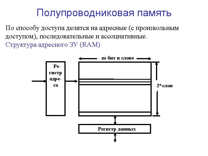
 Semiconductor memory: typically RAM (access time is not depended on")
Random Access Memory (RAM) Semiconductor memory: typically RAM (access time is not depended on data location). RAM: Read-Write memory and ROM (Read-Only memory). Address register Read-write random access memory n bits m bits per word 2 n words Read Write Memory buffer register

Read-Write Memory Two types: SRAM and DRAM SRAM: memory cell – flip-flop DRAM: memory cell – capacity (drain – substrate of MOStransistor). The different types of IC memory organization: • Linear-select (2 D) • Two-dimensional (3 D) • Compromise (2 DM)

Static RAM Store bits in flip-flops. Figure shows a basic memory cell consisting of a flip-flop with associated control circuitry. Select Input S R Write Basic cell for linear-select SRAM Out S I W O

Linear Select SRAM D 3 A 0 A 1 R G DC D 1 D 2 D 0 S I O W S I O W S I O W S I O W Write Read O 3 Four-address memory with 4 bits per word O 2 O 1 O 0
 Select 1 Input Select 2 S T Out R Write Two-dimensional")
Static RAM (2) Select 1 Input Select 2 S T Out R Write Two-dimensional memory cell S 2 S 1 I W O
 The linear-select organization is used for IC memory with small capacity.")
Static RAM (3) The linear-select organization is used for IC memory with small capacity. Address decoder is complicated because there are 2 n AND elements (with n inputs). Address decoder for two-dimensional IC organization is more simple: 2 2 n/2 AND elements (with n/2 inputs). Properties of SRAM: • fast • density is not very large – six transistors per bit • doesn’t need to be refreshed (data stays as long as power is on) • basically used for cache memory
 EN=0 EN A A Y Y EN=1 A module")
Трехстабильный буфер (Three State Buffer) EN=0 EN A A Y Y EN=1 A module tristate (en, a, y); input a, en; output y; reg y; always @ (a or en) begin if (en) y = a; else y = 1’bz; endmodule Out EN 0 0 1 1 A 0 1 Out Z Z 0 1 Или module tristate (en, a, y); input a, en; output y; assign y = en? a: 1’bz; endmodule
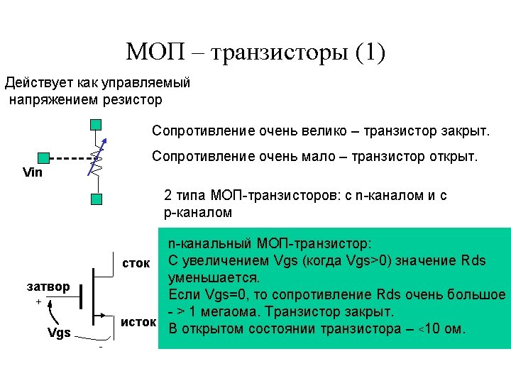

КМОП-инвертор Vdd = +5. 0 V Q 2 Vin Q 1 Q 2 Vout 0. 0 (L) 5. 0 (H) off on On off 5. 0 (H) 0. 0 (L) p-канал Vout Q 1 Vin n-канал IN OUT

SRAM Cell Word Line ~ Bit Line

Структура ЗУ типа 3 D Address n/2 DCY n/2 Address DCX Data

Структура ЗУ с селекторами Ak Row decoder An-1 Memory array 2 n-k m 2 k bits Din (m bits) WR/RD Compromise Data buffers (column I/O) Dout (m bits) CS Column decoder A 0 . . . Ak-1

Static RAM The linear-select organization is used for IC memory with small capacity. Address decoder is complicated: 2 n AND elements (with n inputs). Address decoder for two-dimensional IC organization is more simple: 2 2 n/2 AND elements (with n/2 inputs). Properties of SRAM: • fast • density is not very large – six transistors per bit • doesn’t need to be refreshed (data stays as long as power is on). • basically is used for cache memory

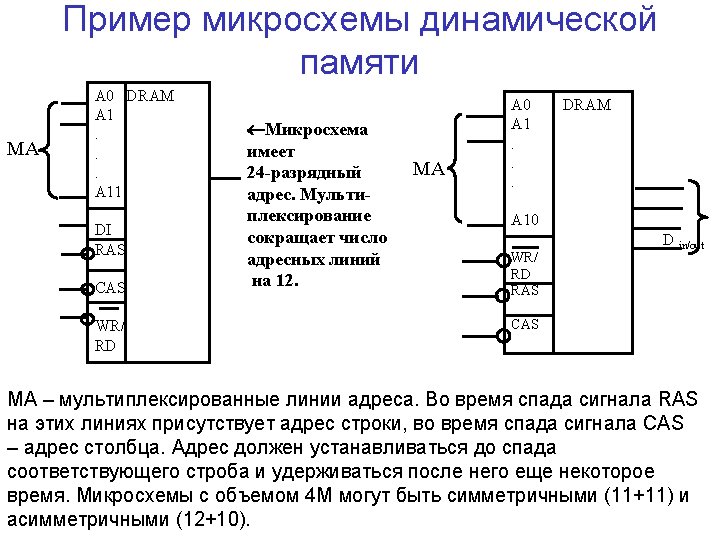
Микросхема статической памяти A 0 A 1 . : . A 14. WE OE CS 0 1. . . 14 W OE CS RAM 0 1 2 3 4 5 6 7 CS OE WE I/Opins Mode 1 x x z Not selected 0 1 1 z Output disable 0 0 1 Dout Read 0 x 0 Din Write

0 1 2 A 3 A 4 A 5 A 6 A 8 A 9 A 11 Memory Array Row Deco -der A 13 Din/out 0 … Din/out 7 CS WE OE 512 8 26 bit 511 Input data control Column I/O Multiplexors A 0 A 1 A 7 A 10 A 12 A 14

Logic Symbols for SRAMs HM 628128 A 0 A 1 A 2. . . A 16 WE CS 1 OE 128 KB IQ 0 IQ 1 IQ 2 IQ 3 IQ 4 IQ 5 IQ 6 IQ 7 HM 628512 A 0 A 1 A 2. . . A 17 A 18 WE CS OE 512 KB IQ 0 IQ 1 IQ 2 IQ 3 IQ 4 IQ 5 IQ 6 IQ 7
 Implement a 1 M× 8 SRAM module using")
Design of SRAM Module (Example 1) Implement a 1 M× 8 SRAM module using 512 K× 8 IC Address bus A 0 A 1. . . A 0. . . ~CS 0 A 18 A 19 Control signals ~WR/RD MEM . . A 18. ~WR ~RD ~WR A 0 . . . A 18 ~CS 0 ~WR ~CS 1 ~RD A 0 D 0 A 18 WE CS OE IQ 0 D 1 IQ 1. . . IQ 7 D 7. . . A 0 A 18 WE CS OE IQ 0 IQ 1. IQ 7 D 0 D 1 . . D 7 D 0 D 1 Data bus D 7 Signal MEM – memory request. Signal ~WR/RD specify operation

Example 2 Implement a 512 K × 16 SRAM module using 128 K× 8 IC A 0 A 1 A 2 A 16 A 17 A 18 MEM ~WR/ RD A 17 0 A 18 1 ~MEM 0 1 2 EN 3 A 0 A 1 A 16 ~WR WE CS 0 CS ~RD OE A 0 A 16 ~WR CS 1 ~RD ~WR A 0 A 16 WE CS OE A 0 A 16 ~WR WE CS 2 CS CS 0 ~RD OE CS 1 CS 2 A 0 A 1 A 16 ~WR WE CS 3 CS CS 3 ~RD OE D 0 D 1 D 7 A 0 A 1 A 16 ~WR WE CS 0 CS ~RD OE A 0 A 1 A 16 WE CS 1 CS ~RD OE A 0 A 1 A 16 ~WR WE CS 2 CS ~RD OE A 0 A 1 A 16 ~WR WE CS 3 CS ~RD OE D 8 D 9 D 15 D 8 D 9 D 0 D 15 D 8 D 9 D 15

SRAM in Verilog RAM inputs & outputs are separate module memory (mem_req, address, data_in, data_out, read_write); input mem_req, read_write; input [3: 0 ] data_in; input [5: 0] address; output reg [3: 0] data_out; reg [3: 0] mem[0: 63]; // 64 4 memory always @(mem_req ) if (mem_req) if (!read_write) mem[address] = data_in; // write else data_out = mem[address]; // read else data_out = 4’bz; // high impedance state endmodule
; input mem_req,")
SRAM in Verilog Bidirectional data bus module memory (mem_req, addr, d_q, read_write); input mem_req, read_write; inout [7: 0 ] d_q; input [7: 0] addr; reg [7: 0] mem[0: 255]; // 256 8 memory assign d_q = mem_req? (read_write ? data[addr] : 8 b’z): 8’z; always @(mem_req or read_write) if(mem_req) if(!read_write) data[addr]=d_q; always (mem_req or data) if(!read_write) data[addr]=d_q; endmodule

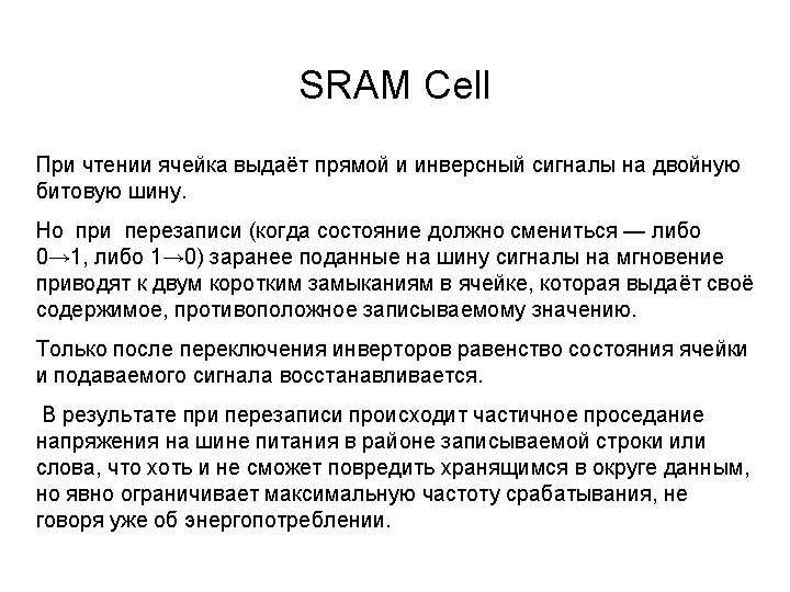
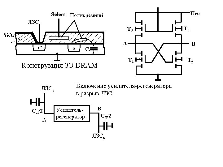
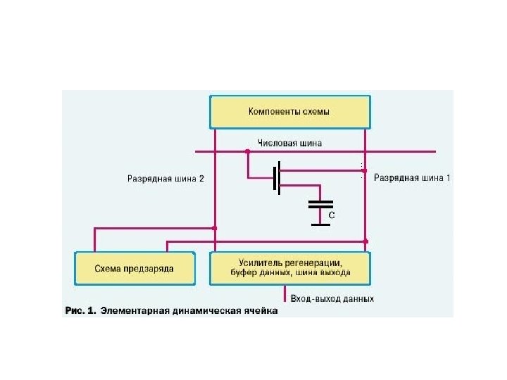
Динамическая память Линия записи/считывания Select Поликремний ЛЗС Si. O 2 n+ n+ Cc Конструкция ЗЭ DRAM Линия выборки (Select) Cл Rн Cç • bit stored as charge in capacitor Cc • high density (1 transistor for DRAM vs 6 transistors for SRAM) • destructive read (capacitor discharge on a read) • read is automatically followed by a write (to restore) • charge leaks away over time (need to refresh)
 “wordline” Select Polysilicon “Bitline” (Data in/out) “wordline” (select) Si.")
Dynamic Random Access Memory (DRAM) “wordline” Select Polysilicon “Bitline” (Data in/out) “wordline” (select) Si. O 2 n+ n+ Cc Cl Rн Cc DRAM memory cell construction • bit stored as charge in capacitor Cc • high density (1 transistor for DRAM vs 6 transistors for SRAM) • destructive read (capacitor discharge on a read) • read is automatically followed by a write (to restore) • charge leaks away over time (need to refresh)

Матрица динамических ЗЭ Row 0 Row 3 Column 0 Column 1 Column 2 Column 3

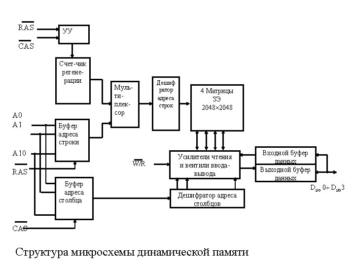
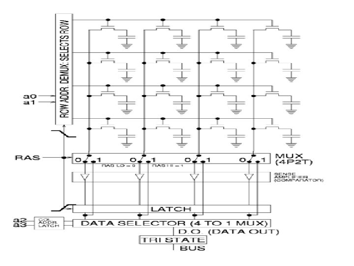
MUX Row decoder A 0. . MUX. An-1 Row address buffer DRAM Chip Organization Memory Array (square matrix) row buffer Din RAS Address WE Column I/O Column decoder CAS Column address buffer Dout

DRAM • multiplexed address lines • internal row buffer • to perform the operation next five cycles are needed: • put row address on lines • set row address strobe (RAS) • read row into row buffer • put column address on line (to switch external multiplexer) • set column address strobe (CAS) • read column bits out of row buffer • write row bits content to row • return RAS and CAS to inactive state

Временные диаграммы DRAM IC Цикл чтения RAS t. RC t. CAS MA WE Цикл ранней записи t. RAS t. RP Row Address Column Address Row Address t. CP t. RCD Column Address t. RAC Data Z t. CAC Data Out Data In t. WCH
 RAS CAS MA 2 способа регенерации")
RAS only refresh (ROR CAS before RAS (CBR) RAS CAS MA 2 способа регенерации : burst refresh, distributed refresh. t. RF= TRF/n 15, 6 мкс t. RF TRF

Comparison SRAM with DRAM • SRAM is faster than DRAM: 1/4 - 1/8 access time of DRAM. • The density SRAM is lower than DRAM 1/4 density of DRAM. • Static: bit is not erased on a read. • SRAM does not need to refresh. • Unlike DRAM, there is no difference between access time and cycle time. Access time: time to read Cycle time: time between reads > access time (DRAM) Cycle time = access time (SRAM) • SRAM address lines are not multiplexed. SRAM is more expensive than DRAM: about 8 -16 times.

• DRAM: “Dynamic” Random Access Memory – Highest densities – Optimized for cost/bit main memory • SRAM: “Static” Random Access Memory – Densities ¼ to 1/8 of DRAM – Speeds 8 -16 x faster than DRAM – Cost 8 -16 x more per bit – Optimized for speed �� caches

DRAM Improvement Year Capacity Access time Cycle time 1980 64 Kb 150 ns 300 ns 1990 1 Mb 80 ns 160 ns 1993 4 Mb 60 ns 120 ns 2000 64 Mb 50 ns 100 ns 2004 1 Gb 45 ns 70 ns 2009 1 Gb 40 ns 50 ns DDR 2: Module Bandwidth – up 10, 6 GB/s


DRAM Optimizations Faster to read data from the same row – Called “page mode” (fast page mode, EDO are variations) – Multiple CAS accesses • Bandwidth determined by cycle time – Example Row: 100 ns + – Example Column: 30 ns +, usually more like 50 ns due to external components • Add a clock to the interface - synchronous DRAMs – Enable split transactions • Use both edges of the clock - Double data rate In practice – There are multiple banks on chip – Arrays are 1 -4 Mbits
 Q 1: Where can a block")
Four Memory Hierarchy Questions (4 вопроса иерархии памяти) Q 1: Where can a block be placed in a cache? (block placement) Q 2: How is a block found if it is in a cache? (block identification) Q 3: Which block should be replaced on a miss? (block replacement) Q 4: What happens on a write? (write strategy). • If each block has only one place it can appear in the cache, the cache is said to be direct mapped. • If a block can be placed anywhere in the cache, the cache is said to be fully associative. • If a block can be placed in a restricted set in the cache, the cache is said to be set associative. If ther are n blocks in a set – is called n-way associative.

Понятия Hit: data appears in some block in the cache. Miss: data needs to be retrieve from a block in the DRAM. Hit time: RAM access time +time to determine hit/miss. Miss Rate = 1 - Hit Rate; Miss Penalty: Time to replace a block in the cache + Time to deliver the block the processor. Hit time << Miss Penalty.
 For a cache of 2 M bytes with block")
Direct Mapped Cache (cont. ) For a cache of 2 M bytes with block size of 2 L bytes: 32 -M bits Tag M-L bits Index L bits Block Offset 31 0 Address Example: For a cache of 32 K bytes with block size of 64 bytes: 17 bits Tag 9 bits Index 31 6 bits Block Offset 0 Address

Direct Mapped Cache Block Address 17 bits 9 bits 04440 h 6 bits 0000001 b Block Offset 31 0 Valid 1 1 Cache Tags Cache Data Byte 63 Byte 0 04440 == Hit MUX

Block Address 19 bits 7 bits 00 x 0050 6 bits 0000001 Block Offset 31 0 Valid 1 1 Cache Tags Cache Data Byte 63 Byte 0 00 x 00650 == Miss MUX
, содержит всего 1")
Преимущества Direct Mapped Cache – схема достаточно простая (небольшое число транзисторов), содержит всего 1 компаратор. Cache block is available before Hit/Miss. Недостаток – частые Cache-промахи Block Size Tradeoff: Larger block size takes advantage of spatial locality, but: Larger block size means larger miss penalty.
 Tag (номер блока) Смещение (Offset) Tags == ==")
Полностью ассоциативная кэш-память (Fully Associative Cache) Tag (номер блока) Смещение (Offset) Tags == == Data Hit/Miss Each block can be placed anywhere in the cache.
 is very")
Disadvanteges of fully associative cache: The number of comparators (number of entries) is very large. Достоинство – блок удаляется только тогда, когда заполнена вся память.

ОП 4 -way set-associative Cache 5 4 3 2 1 0 Cache directory 2 5 3 0 0 4 1 3 0 3 4 5 2 1 2 641 513 385 257 129 1 642 643 514 515 386 387 258 259 130 131 2 3 767 639 511 383 255 127 0 1 2 127 256 640 384 0 513 129 385 1 386 514 642 258 1 2 == == 0 . . . 127 Tag Номер набора. . 3 Comparators 2 3 0 4 31 640 512 384 256 128 0 . 12 11. . . 5 4 383 511 127 639. . . 127 Смещение. . . 0

Disadvanteges of set-associative cache: N-way set-associative cache contains N comparators. Data comes after Hit/Miss decision and set selection. Advantages: each memory block has choice of N cache lines. Для каждого блока есть выбор из N позиций. Зависимость между объемом кэш-памяти V (Cache size), размером блока Z(block size), числом каналов w (associativity) и числом наборов S выражается следующей формулой: V = w S Z.
 Tag Index Offset The number of sets S=2")
Set-Associative Cache Direct-mapped cache (1 -way) Tag Index Offset The number of sets S=2 S 0 DC S 1 == MUX Hit? Data
 Tag w 0 w 1 w 2 Index w")
4 -way Set-Associative Cache (example) Tag w 0 w 1 w 2 Index w 3 Offset w 0 w 1 w 2 w 3 S 0 DC DC S 1 == == S 1 MUX MUX Hit? MUX CD Data The number of sets S=2 Why SA is slow MUX

Cache Block Replacement Policy Random Replacement: Hardware Randomly Selects a cache item and throw it out. Least Recently Used: -Hardware keeps track of the access history. Replace the entry that has not been used for the longest time.

Cache Write Policy Write Through: Write to cache and memory at the same time. Write Back: Write only Cache. Write Buffer for the Write Through. Victim Cache.

Multi-Level Cache GPRs L 1: 32 K + 32 K, 8 -way - Intel (Conroe) L 1 I L 1 D 64 K + 64 K, 2 -way - AMD K 8 Block size – 64 byte. L 2 – P 4 -E(Prescott), 2 Mbyte, Conroe – 4 M Itanium Montecito L 2 – 512 Kbyte, L 3 – 24 Mbyte L 3 Sandy Bridge L 2 – 512 K Byte, L 3 – 8 M Byte
")
Average Memory Access Time (AMAT)

Disk Parameters
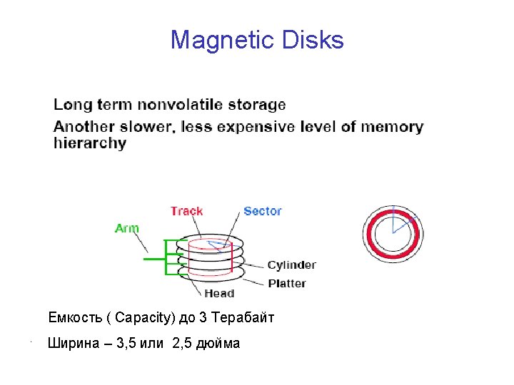

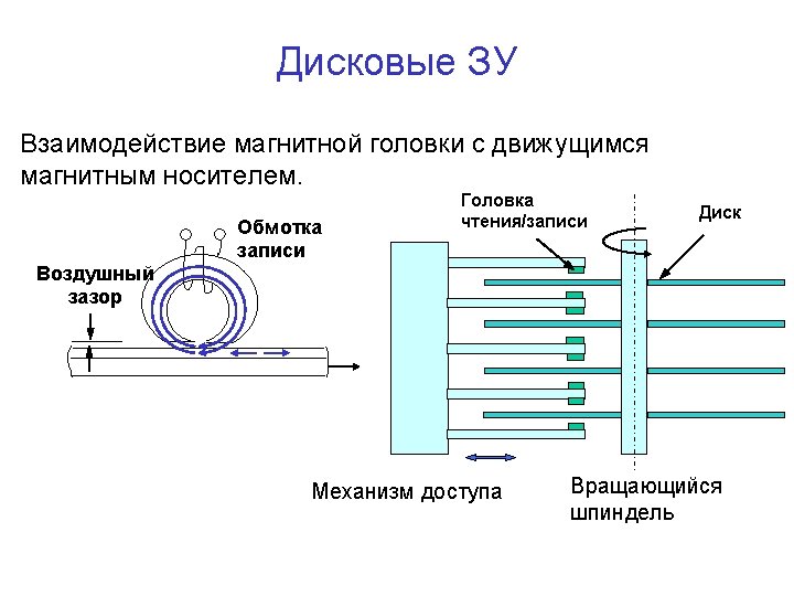
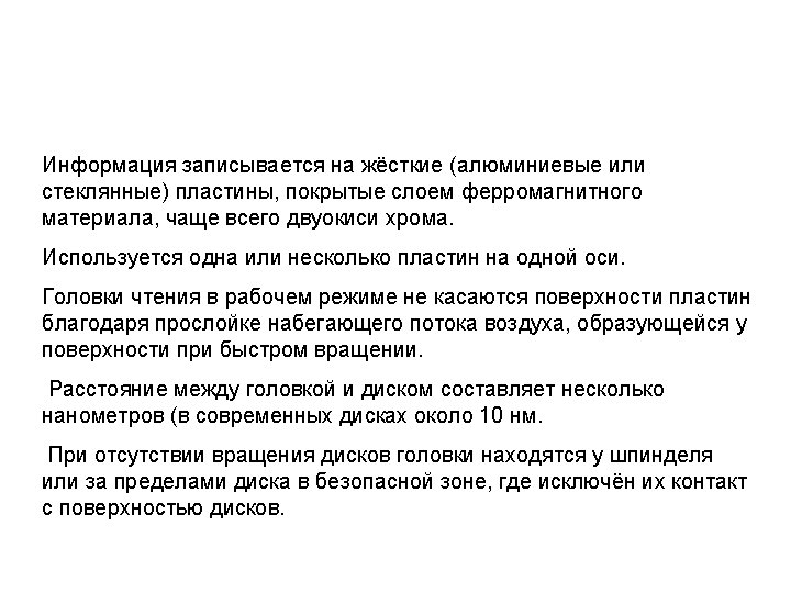
Magnetic Disks

Disk Performance

Формат дорожки диска Sector 0 GAP 1 ID 17 7 GAP 2 Sector 1 DATA GAP 3 GAP 1 ID 41 515 Synch Data 20 CRC GAP 2 DATA GAP 3

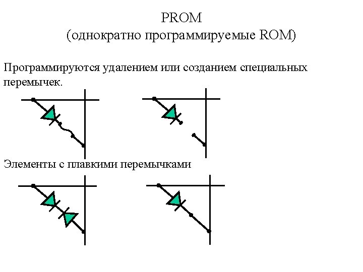
Programmable ROM A PROM chip is manufactured with all of its diodes or transistors “connected”. The customer may program the ROM using PROM programmer. OR Matrix DC 0 1 2 3 4 5 6 7 Fuse A link is vaporized by selecting it using PROM address and data lines and then applying a high voltage pulse (10 -30 V) to the device through a special input pin (for programming).

Programmable ROM Programmed by removing or creating special links. “ 1” “ 0” WL BL BL WL “ 1” “ 0” BL BL

ROM cells VDD “ 1” “ 0” Bit Line BL WL Word Line BL BL WL WL GND

Application of MOS Transistors as Memory VDD Cells Active high word line A 0 DC A 1 An-1 ~ D 0 ~D 1 ~D’ 7 Active low bit lines

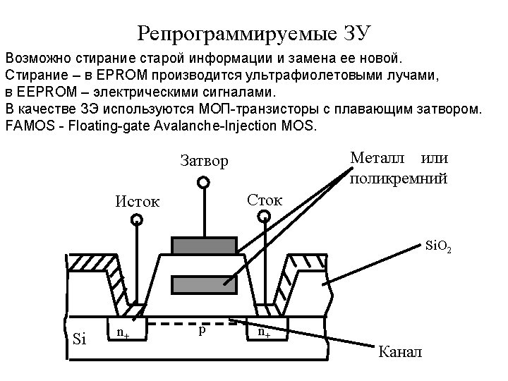
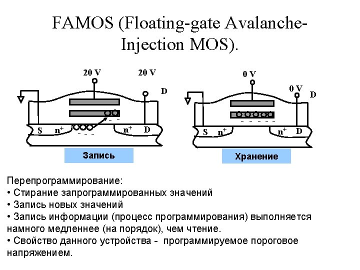
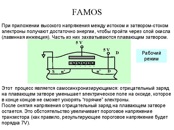
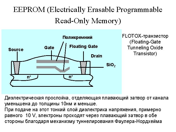
Erasable PROM Erasing of old information and its replacement with the new one is possible. Erasing is carried out by ultraviolet rays in EPROM (erasable PROM), In EEPROM (electrically PROM) – by electrical signals. Floating gate MOS transistors are used as connection links. Polysilicon Floating gate Gate Drain Source G S Si. O 2 n D + Substrate p Si Device cross-section n +

Storage Matrix in EPROM VDD Active-high word lines Active-low bit lines

EEPROM A 0 A 14 CS OE Q 0 Q 1 Q 2 Q 3 Q 4 Q 5 Q 6 Q 7

Organization of IC size 32 Kx 8 A 6 0 1 511 DC Matrix 512 x 64 Matrix 512 x 64 64 -1 MUX 64 -1 MUX D 5 D 4 D 3 D 2 D 1 A 14 A 0 A 5 D 7 D 6 D 0

Using ROM for Realization of Integer Multiplication A 7 A 6 A 5 A 4 A 3 A 2 A 1 A 0 Q 7 Q 6 Q 5 Q 4 Q 3 Q 2 Q 1 Q 0 A 1 A 2 A 3 B 0 B 1 B 2 B 3 A 0 A 1 A 2 A 3 A 4 A 5 A 6 A 7 Q 0 Q 1 Q 2 Q 3 Q 4 Q 5 Q 6 Q 7 CS A, B – 4 -bit integer unsigned A= (a 3 a 2 a 1 a 0) B=(b 3 b 2 b 1 b 0) A×B = P Y 1 Y 2 Y 3 Y 4 Y 5 Y 6 Y 7 Y 8 B 3 B 2 B 1 B 0 A 3 A 2 A 1 A 0 P 7 P 6 P 5 P 4 P 3 P 2 P 1 P 0 0 0 0 0 0 1 0 0 0 0 0 0 1 1 1 0 0 0 1 0 1 0 0 1 1 1 0 0 0 1 1 1 0 0 0 1 1 1 1 0 1 1 1 0 0 1 1 1 1 1 0 1 1 1 0 0 1
 X 8 X 7 X 6")
Using ROM for Realization of logic Functions (LUT) X 8 X 7 X 6 X 5 X 4 X 3 X 2 X 1 A 0 A 1 A 2 A 3 A 4 A 5 A 6 A 7 CS Q 0 Q 1 Q 2 Q 3 Q 4 Q 5 Q 6 Q 7 Y 1 Y 2 Y 3 Y 4 Y 5 Y 6 Y 7 Y 8 x 1 x 2 x 3 x 4 x 5 x 6 x 7 x 8 y 1 y 2 y 3 y 4 y 5 y 6 y 7 y 8 0 0 0 0 0 1 0 0 0 1 1 0 1 0 0 0 0 0 1 0 0 0 0 0 1 1 1 0 0 0 1 0 0 0 1 1 0 0 1 0 1 1 1 1 0 1 1 0 0 1 0 1 1 1 1 0 0 1 1 1 0 0 1
 X 1 X 2 X 3 X")
Использование ROM для реализации логических функций (LUT) X 1 X 2 X 3 X 4 X 5 X 6 X 7 X 8 0 1 2 3 4 5 6 7 Y 1 Y 2 Y 3 Y 4 Y 5 Y 6 Y 7 Y 8 A 3 A 2 A 1 A 0 B 3 B 2 B 1 B 0 0 1 2 3 4 5 6 7 P 6 P 5 P 4 P 3 P 2 P 1 P 0

A 18 -0 DQ 15/A 1 DQ 14 -0 CE OE WE DATA RP Reset Vcc Vpp GND Boot-Block Flash. Memory В главных блоках хранятся основные управляющие программы

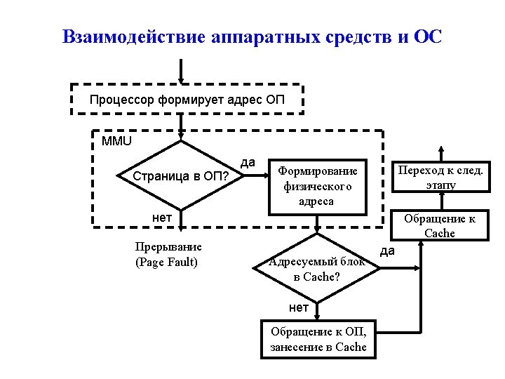
Виртуальная память MMU – memory management unit Processor Data Virtual Address MMU Physical Address Cache Data Physical Address Main Memory Swapping, Replacement Magnetic Disk Storage

Страничная организация памяти Physical Memory Virtual Memory Block 0 Page 0 P Номер блока Page 1 Page 2 Page 3 Page 4 0 1 2 3 4 5 1 1 0 0 1 3 2 Block 1 Block 2 Block 3 Page 5 2047 Block 63 Page 2047 Disk
 Virtual Address 31 . . .")
Translation of VA to PA (VPN to PFN) Virtual Address 31 . . . 21 20 Page Number . . . 0 Page Offset Page Table 0 1 1 1 2 0 1 1 3 2 2047 28 . . . 21 20 Frame Number . . . Page Offset Physical Address 0
 associative •")
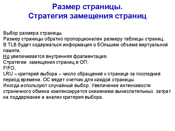
Virtual Memory: The Four Question • Page placement: fully (or very highly) associative • Page identification: address translation • Page replacement: sophisticated (LRU + “working set”) • Write Strategy: Write – back. Write back reduces a disk traffic. Disk is the backing store for the main memory. Memory is 50 to 100 times slower than processor. Disk is 200 to 1000 times slower than memory. Disk is 1 to 10 million times slower than processor. VA miss (VPN has no PFN) is called “page fault”. Page “penalty” is very large – 1. 000 to 10. 000 clock cycles. Page size is usually large: 4 KB – 16 KB, 2 MB

Flow Chart for Virtual Memory system with Cache Memory Processor forms VA MMU Is the page in a memory? Yes The next stage of instruction execution Translation VA to PA Send data to address No Page Fault Yes Cache hit? No Update Cache
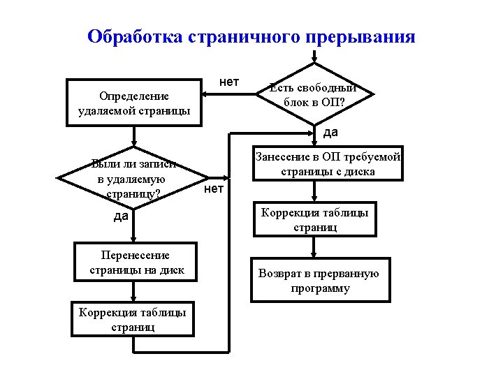
 Entry of Page Fault routine Exercise memory replacement algorithm Yes Was")
Flow Chart (2) Entry of Page Fault routine Exercise memory replacement algorithm Yes Was the page updated? Yes Write the page from memory to disk Page table update No Is main memory full? No Read the page from disk to memory Page table update Return to instruction that was halted
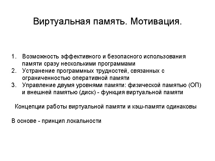
 Page tables are usually so large that are stored in main")
Page Tables (PT) Page tables are usually so large that are stored in main memory (OS forms page tables for each process). A page table is an array of PTEs (Page Table Entries). PTE format Page Table PT Root P PTE PVN PFN D R/W A P – Present D – Dirty R/W – Write protection A – Accessed

Virtual Memory for Different Processes Virtual address space Physical memory 0 0 Process i N-1 VP 2 Common page frame 0 Process j N-1 VP 2 M-1

Page Table Size The page size is inversely proportional to the page table size. Example 1: 32 -bit VA, 4 KB pages, 4 -byte PTE. • 1 M pages (4 Gbyte/4 Kbyte = 220 pages) • 1 M*4 bytes = 4 Mbyte – page table size (it is very large, but can be more). Example 2: 64 -bit VA, 4 KB pages, 4 -byte PTE. • 4 P pages (264/212=252 pages) • 16 P bytes – page table size (it is impossible to realize). The methods to reduce page size: • multi-level page tables • inverted page tables

Multi-level Page Tables Use tree of page tables. Example: two-level organization in Intel processors. 31 22 21 Directory 12 11 Table 2 nd 10 1 st level table 10 level table 0 Offset 12 data PA PTE PDBR 1 st level table (PDEs) points the 2 -level table. 2 nd level table (PTEs) points data. “+” - save memory space. “-” - slow (multi-hop chain of translations). Alpha 21264 has three level of page tables.

Inverted Page Tables Alternative approach: PVN maps by hash function on hash table, that contains pointer to inverted page frame. Advantages: Don’t need more PTEs that physical memory pages. Can appear collisions (more than one PVN use the same element of hash table). In this case chained list is used. PVN Hash Function Offset PVN 1 PVN 2 PTE Pointer PFN Offset
 Virtual Address Page Number (PVN) TLB Page Number No Offset")
Translation Look-Aside Buffer (1) Virtual Address Page Number (PVN) TLB Page Number No Offset Block Number Control (PFN) bits = ? Yes Miss Hit Block Number (PFN) Offset Physical Address
 Virtual Address Page Number (PVN) Offset TLB Tag PVN 1 PVN 2")
TLB (2) Virtual Address Page Number (PVN) Offset TLB Tag PVN 1 PVN 2 PVN 3 PVNK == V D R/W A Block Number (PFN) == == Block Number (PFN) Offset Physical Address
 Paging means, that every memory access logical takes at least")
Translation Look-Aside Buffer (3) Paging means, that every memory access logical takes at least twice as long, with one memory access to obtain the physical address and second access to get the data. Fast address translation: solution – to again rely on the principle of locality. The usage of TLB is allowed to decide this problem. TLB – usually fully associative cache for PTE. TLB miss: entry not in TLB, but in page table (soft miss) • Not quite a page fault (no disk access necessary). • Page fault: entry not in TLB and not in page table.
 TLB Control Tag V bits VPN 1 1 TLB Hit Page Frame")
TLB (4) TLB Control Tag V bits VPN 1 1 TLB Hit Page Frame Number 0 8 5 12 0 0 1 11 4 TLB Miss 1 1 1 0 1 0 8 0 9 7 10 2 11 4 12 5 13 Page Table 0 1 2 3 4 5 6 7 8 Physical Memory 8 14 10 11 12 9 14 1 15 Disks
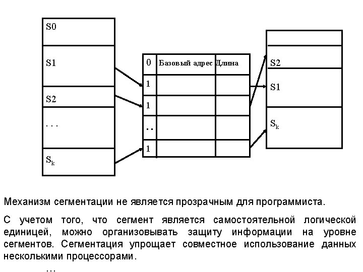
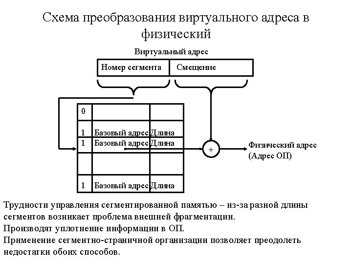

Intel Pentium Segmentation Virtual Address Seg Selector Offset Segment Descriptor Main Memory Segments
- Slides: 179