INTEGRATOR Integrator The basic integrator is easily identified

INTEGRATOR

Integrator The basic integrator is easily identified by the capacitor in the feedback loop. A constant input voltage yields a ramp output. The input resistor and the capacitor form a RC circuit. The slope of the ramp is determined by the RC time constant. The integrator can be used to change a square wave input into a triangular wave output.

The capacitive impedance: Integrator The input current: Thus the output in time domain: Rate of change of the output:

The output voltage: - Vout is the same as the voltage on the negative side of the capacitor - When constant positive input voltage (step or pulse) is applied, the output ramp decreases negatively until the op-amp saturates at its maximum level Usefulness: - Especially use in triangular-wave oscillators

Example C = 0. 01 F Vin R = 10 k +2. 5 V Vout -2. 5 V a) Determine the rate of change of the output voltage in response to the input square wave. The output voltage is initially zero. The pulse width is 100 s. b) Draw the waveform.
 - during capacitor charging - during capacitor discharging")
Solution a) - during capacitor charging - during capacitor discharging
 + 2. 5 V Vin - 2. 5 V 0 Vout - 5")
b) + 2. 5 V Vin - 2. 5 V 0 Vout - 5 V 100 s

Real Integrator CF RF Vin +V R 1 Vout RP -V RP : added to the noninverting input to balance the effects of bias current (usually the value is similar to R 1) RF : provides the dc feedback and overcome the saturation problem, i. e. to reduce the error voltage at the output

DIFFERENTIATOR

Differentiator The differentiator does the opposite of the integrator in that it takes a sloping input and provides an output that is proportional to the rate of change of the input. Note the capacitor is in the input circuit. The output voltage can be determined by the formula below.

How it works C Vin i. C R Vout i. R ------> Eqn. 1 ------> Eqn. 2
 When")
When input is a positive-going ramp, the output is negative (capacitor is charging) When input is a negative-going ramp, the output is positive (capacitor is discharging) – current is the opposite direction

Example R 2. 2 k C + 5 V Vin 10 s 0 5 s 15 s t 0. 001 F - 5 V Determine the output voltage of the op-amp differentiator for the triangular-wave input shown. Vout

Solution § At t = 0, Vin is a positive-going ramp ranging from -5 V to +5 V (i. e. +10 V change) in 5 s § From t = 5 s to 10 s, Vin is a negative-going ramp ranging from +5 V to -5 V (i. e. -10 V change) § time constant, RC = (2. 2 k)(0. 001 ) = 2. 2 s § the slope, VC / t = 10 V/ 5 s = 2 V/ s (+ve ramp) (-ve ramp)

Output waveform Vin 0 t +4. 4 V Vout 0 -4. 4 V 5 s 10 s 15 s t

A Practical Differentiator CF RF Vin R C Vout RP n A shunt capacitor and a series resistor are added – to reduce high frequency noise
")
COMPARATOR (part I)

Comparator n n The comparator is an op-amp circuit that compares two input voltages and produces an output indicating the relationship between them. The inputs can be two signals (such as two sine waves) or a signal and a fixed dc reference voltage. Comparators are most commonly used in digital applications. Digital circuits respond to rectangular or square waves, rather than sine waves. These waveforms are made up of alternating (high and low) dc levels and the transitions between them.

Comparator n n Assume that the digital system is designed to perform a specific function when a sine wave input reaches a value of 10 V. Using a comparator between the signal source and the digital system, as shown below, solves the problem.
 v COMPARATOR WITH ZERO REFERENCE v COMPARATOR WITH NONZERO REFERENCE")
COMPARATORS (part II) v COMPARATOR WITH ZERO REFERENCE v COMPARATOR WITH NONZERO REFERENCE

NONLINEAR CIRCUITS q Nonlinear circuits such as comparators, wave shapers and active-diode circuits. q Linear circuits like voltage amplifier, current sources, and active filters. q The output of nonlinear op-amp circuits usually has a different shape from the input signal. This is due to the op-amp saturates during part of the input cycle.

ZERO REFERENCE q The simplest way to build a comparator is to connect op-amp without feedback resistors. Vout +V Vin +Vsa t Vout -V a) Comparator with zero reference 0 -Vsat b) Input/output response Vin

n n n Because of the high open-loop gain, positive input voltage produces positive saturation (+Vsat), and a negative input voltage produces negative saturation (Vsat). This comparator is called a zero-crossing detector. The minimum input voltage that produces saturation is:

n If a sinusoidal input voltage applied to the noninverting input of this circuit, the result will look like this: Vi n 0 Vou t t +Vsat 0 t -Vsat

Example n Let Vsat = 15 V, Aol = 100, 000. Then the input voltage needed to produce saturation is:

Solution Vin > +0. 015 m. V +Vsat Vin < -0. 015 m. V -Vsat

The output is a two-state output, either +Vsat or –Vsat n This comparator can be used as a squaring circuit (i. e. produce square wave from sine wave). n

Bounded Output n n n The output swing of a zero-crossing detector may be too large in some applications. In some applications, necessary to limit the output voltage levels of comparator to a value less than provided by the saturated op-amp. We can bound the output by using a zener diode – limit the output voltage to the zener voltage in one direction

Bounded at positive value +Vz Dz Vin R +V 0 Vout -0. 7 V -V n When output voltage reaches positive value equal to the zener voltage – limit at that value

Bounded at negative value Dz Vin R Vout -V n +0. 7 V +V 0 -Vz When output switches negative, zener acts as a regular diode and becomes forward biased at 0. 7 V – limiting the negative output voltage

Double-bounded Dz 1 Vin R Dz 2 +V Vz 2 + 0. 7 V Vout 0 - (Vz 1 + 0. 7 V) n -V Two zener diodes arranged – limit the output voltage to the zener voltage plus forward biased 0. 7 V (positively and negatively)

NON-ZERO REFERENCES n In some applications a threshold voltage different from zero may be preferred. By biasing either input, we can change threshold voltage as needed.

Positive Threshold +V Vout R 1 +V +Vsat Vref R 2 Vout Vin -V Vref Vin -Vsat • When Vin > Vref, Vout is High (+Vsat) • When Vin < Vref, Vout is Low (-Vsat)

Negative threshold n If a negative limit is preferred, connect –V to the voltage divider. Vout +Vs at Vref Vsat Vin • When Vin > Vref, Vout is High (+Vsat) • When Vin < Vref, Vout is Low (-Vsat)

Using Zener diode +V Vref R +V Vz Vin t Vout Vin -V +Vout( max) Vout t Vout(m in) Zener diode is used to set the VREF = VZ Vin < VREF, output remains at the maximum negative level Vin > VREF, output goes to maximum positive level
 v COMPARATOR WITH HYSTERESIS")
COMPARATORS (part III) v COMPARATOR WITH HYSTERESIS

Effect of Noise on Comparator circuits Vin Without noise 0 With noise t Vout +Vsat 0 -Vsat t False output changes due to noise

Effect of Noise on Comparator circuits -Noise (unwanted voltage fluctuations appears on the input line) - Noise can cause a comparator to erratically switch output states

- When sine waves approaches zero, the fluctuation cause the total input vary above and below zero times – produce an erratic output voltage

How to reduce noise effect n n n Effects of noise on a zero-crossing detector One way to reduce the effect of noise is by using a comparator with positive feedback This circuit is usually called a Schmitt trigger The positive feedback produces two separate trip points that prevent a noisy input from producing false transitions (i. e. UTP and LTP) – Hysteresis UTP – upper trigger point LTP – lower trigger point

Schmitt trigger symbol q The symbol for Schmitt triggers in electronic diagrams is a triangle with a hysteresis symbol:

SCHMITT TRIGGER +V Vin Vout -V R 1 R 2
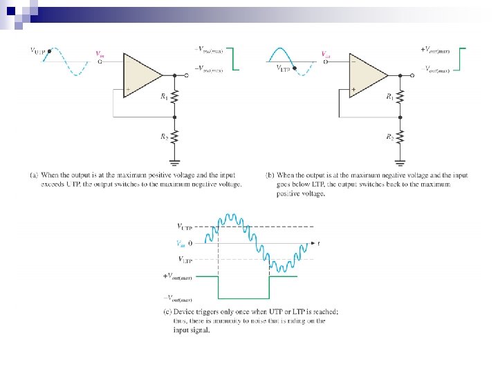

What is Hysteresis? n n The difference in voltage between VUTP and VLTP is called hysteresis voltage, VHYS Whenever any circuit changes from one state to second state at some input signal and then reverts from the second state to the first state at a different input signal, the circuit is said to exhibit hysteresis.

Comparators Application Over-Temperature Sensing circuit

Purpose of the circuit is to determine when the temperature reaches a certain critical value The circuit consist of Wheatstone Bridge with the op-amp used to detect when the bridge is balanced Thermistor (R 1) – temperature sensing resistor (resistance decrease as temperature increase) Potentiometer (R 2) – set at value equal to the R 1 at the critical temperature Below critical value – R 1>R 2 (creating unbalanced condition that drives the op-amp to its low saturated output level and keeps transistor Q 1 off) Reaches critical value – R 1=R 2 (bridge becomes balanced since R 3=R 4) Op-amp switches to high saturated output level and turning Q 1 on. Energize the relay and activate the alarm.

Comparators Application Analog to Digital Converter

n n n A/D conversion is a common interfacing process used when a linear analog system must provide inputs to a digital system The simultaneous or flash method of A/D conversion uses parallel comparators to compare the linear input signal with various reference voltages developed by voltage divider Input voltage exceeds the reference voltage for given comparator, high level is produced on that comparator’s output The reference voltage for each comparator is set by the resistive voltage divider and VREF The priority encoder produces 3 digit binary numbers on its output which represent the values of the analog input voltage.

Summary ØThe summing amplifier’s output is the sum of the inputs. ØAn averaging amplifier yields an output that is the average of all the inputs. Ø The scaling adder has inputs of different weight with each contributing more or less to the input. Ø Integrators change a constant voltage input to a sloped output Ø Differentiators change a sloping input into a step voltage proportional to the rate of change. ØThe op-amp comparator’s output changes state when the input voltage exceeds the reference voltage.
- Slides: 49