Integration of DFT Process and Device Modeling The

- Slides: 9

Integration of DFT, Process and Device Modeling: The Virtual Fab University of Maryland Neil Goldsman Dev Ettisserry, Chris Darmody & Akin Akturk Army Research Lab Aivars Lelis, Dan Habersat & Ron Green

Integration of DFT, Process and Device Modeling: The Virtual Fab Outline 1. Neil Goldsman a) Summary of Virtual Fab Simulation Platform b) Conclusions on The Mobility c) Key Density Functional Theory Results on Atomic Defects: Reliability and Mobility 2. Dev Ettisserry a) Integrated DFT Modeling b) Hole Traps and E’ Centers c) Process Development

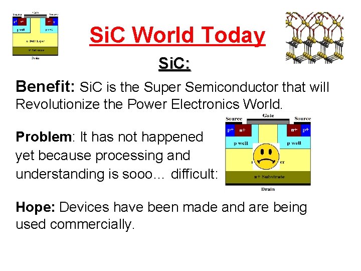
Si. C World Today Si. C: Benefit: Si. C is the Super Semiconductor that will Revolutionize the Power Electronics World. Problem: It has not happened yet because processing and understanding is sooo… difficult: Hope: Devices have been made and are being used commercially.

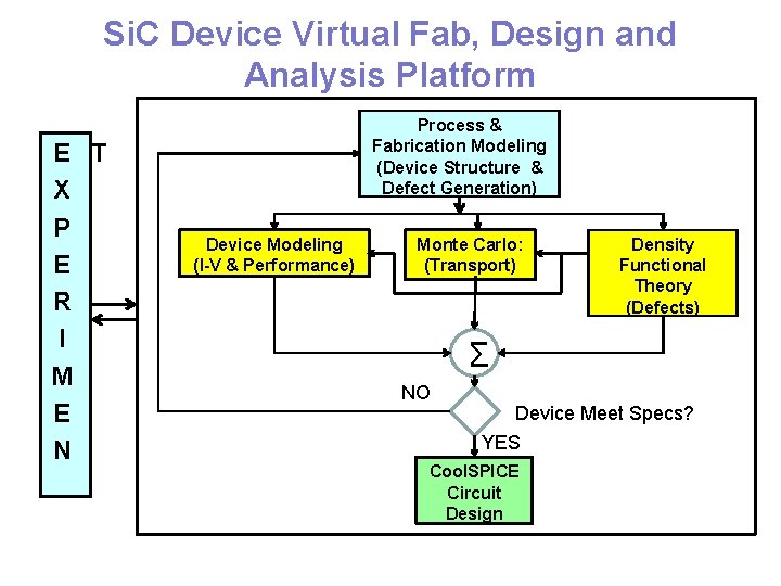
Si. C Device Virtual Fab, Design and Analysis Platform E T X P E R I M E N Process & Fabrication Modeling (Device Structure & Defect Generation) Device Modeling (I-V & Performance) Monte Carlo: (Transport) Density Functional Theory (Defects) Σ NO Device Meet Specs? YES Cool. SPICE Circuit Design

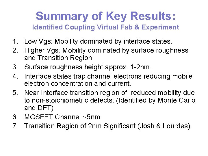
Summary of Key Results: Identified Coupling Virtual Fab & Experiment 1. Low Vgs: Mobility dominated by interface states. 2. Higher Vgs: Mobility dominated by surface roughness and Transition Region 3. Surface roughness height approx. 1 -2 nm. 4. Interface states trap channel electrons reducing mobile electron concentration and current. 5. Near Interface transition region of reduced mobility due to non-stoichiometric defects: (Identified by Monte Carlo and DFT) 6. MOSFET Channel ~5 nm 7. Transition Region of 2 nm Significant (Josh & Lourdes)

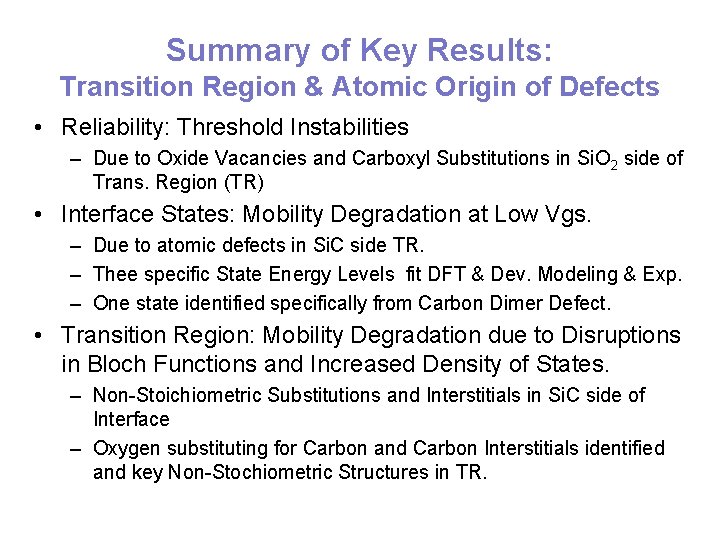
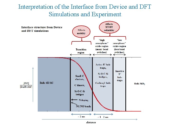
Summary of Key Results: Transition Region & Atomic Origin of Defects • Reliability: Threshold Instabilities – Due to Oxide Vacancies and Carboxyl Substitutions in Si. O 2 side of Trans. Region (TR) • Interface States: Mobility Degradation at Low Vgs. – Due to atomic defects in Si. C side TR. – Thee specific State Energy Levels fit DFT & Dev. Modeling & Exp. – One state identified specifically from Carbon Dimer Defect. • Transition Region: Mobility Degradation due to Disruptions in Bloch Functions and Increased Density of States. – Non-Stoichiometric Substitutions and Interstitials in Si. C side of Interface – Oxygen substituting for Carbon and Carbon Interstitials identified and key Non-Stochiometric Structures in TR.

Interpretation of the Interface from Device and DFT Simulations and Experiment

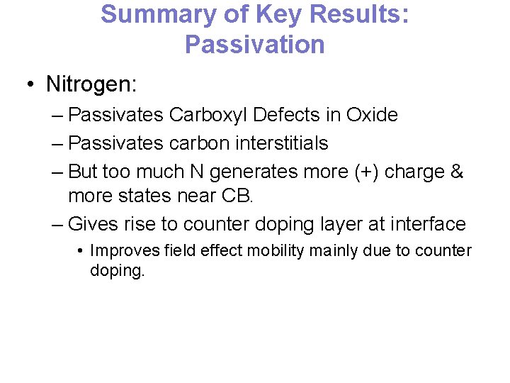
Summary of Key Results: Passivation • Nitrogen: – Passivates Carboxyl Defects in Oxide – Passivates carbon interstitials – But too much N generates more (+) charge & more states near CB. – Gives rise to counter doping layer at interface • Improves field effect mobility mainly due to counter doping.

Si. C Device Virtual Fab, Design and Analysis Platform Questions? Next, Dev Ettissery will explain new reliability work on atomic origin of E’ centers in Si. O 2 Virtually all results have been published in JAP an IEEE with details provided.