Integration of cache System into MIPS Pipeline Datapath

- Slides: 7

Integration of cache System into MIPS Pipeline • Data-path control unit design • Pipeline stalls on cache misses 2022/1/20 coursecpeg 323 -08 FTopic 7 d 1

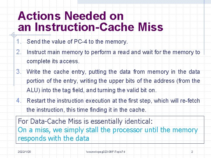
Actions Needed on an Instruction-Cache Miss 1. Send the value of PC-4 to the memory. 2. Instruct main memory to perform a read and wait for the memory to complete its access. 3. Write the cache entry, putting the data from memory in the data portion of the entry, writing the upper bits of the address (from the ALU) into the tag field, and turning the valid bit on. 4. Restart the instruction execution at the first step, which will re-fetch the instruction, this time finding it in the cache. For Data-Cache Miss is essentially identical: On a miss, we simply stall the processor until the memory responds with the data 2022/1/20 coursecpeg 323 -08 FTopic 7 d 2

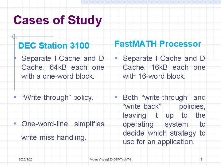
Cases of Study Fast. MATH Processor DEC Station 3100 • Separate I-Cache and D- • Separate I-Cache and DCache. 64 k. B each one with a one-word block. • “Write-through” policy. • One-word-line simplifies write-miss handling. 2022/1/20 Cache. 16 k. B each one with 16 -word block. • Both “write-through” and “write-back” policies, leaving it up to the operating system to decide which strategy to use for an application. coursecpeg 323 -08 FTopic 7 d 3

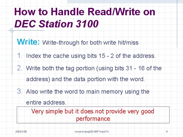
How to Handle Read/Write on DEC Station 3100 Write: Write-through for both write hit/miss 1. Index the cache using bits 15 - 2 of the address. 2. Write both the tag portion (using bits 31 - 16 of the address) and the data portion with the word. 3. Also write the word to main memory using the entire address. Very simple but it does not provide very good performance 2022/1/20 coursecpeg 323 -08 FTopic 7 d 4

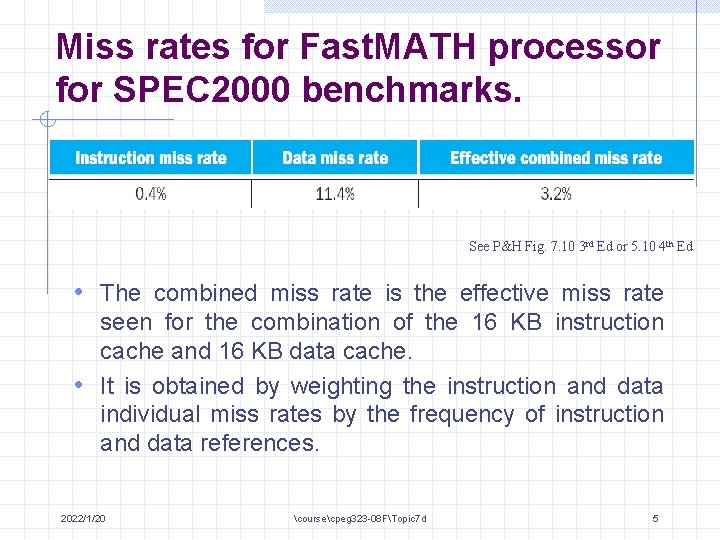
Miss rates for Fast. MATH processor for SPEC 2000 benchmarks. See P&H Fig. 7. 10 3 rd Ed or 5. 10 4 th Ed • The combined miss rate is the effective miss rate seen for the combination of the 16 KB instruction cache and 16 KB data cache. • It is obtained by weighting the instruction and data individual miss rates by the frequency of instruction and data references. 2022/1/20 coursecpeg 323 -08 FTopic 7 d 5

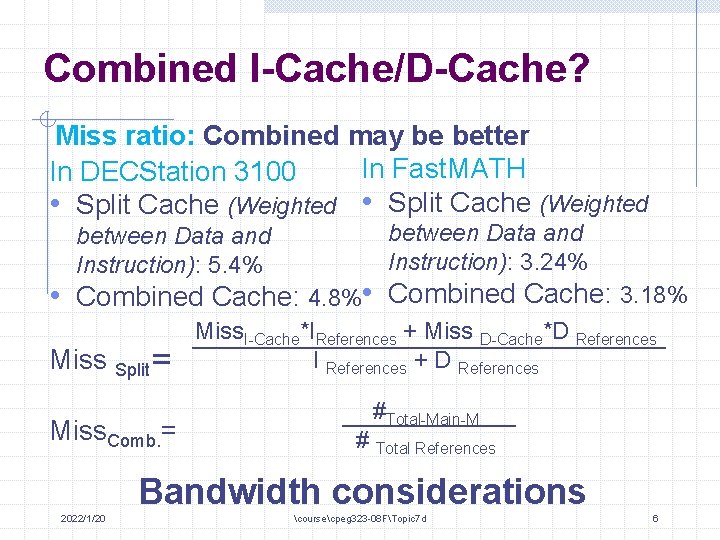
Combined I-Cache/D-Cache? Miss ratio: Combined may be better In Fast. MATH In DECStation 3100 • Split Cache (Weighted between Data and Instruction): 5. 4% between Data and Instruction): 3. 24% • Combined Cache: 4. 8% • Combined Cache: 3. 18% Miss Split= Miss. Comb. = Miss. I-Cache*IReferences + Miss D-Cache*D References I References + D References #Total-Main-M # Total References Bandwidth considerations 2022/1/20 coursecpeg 323 -08 FTopic 7 d 6

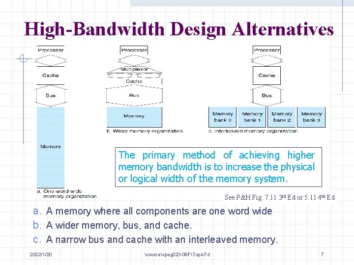
High-Bandwidth Design Alternatives The primary method of achieving higher memory bandwidth is to increase the physical or logical width of the memory system. See P&H Fig. 7. 11 3 rd Ed or 5. 11 4 th Ed a. A memory where all components are one word wide b. A wider memory, bus, and cache. c. A narrow bus and cache with an interleaved memory. 2022/1/20 coursecpeg 323 -08 FTopic 7 d 7