Integrated Circuits packaging PHESE Seminar David Porret PHESEME
- Slides: 37

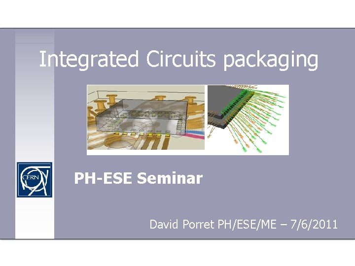
Integrated Circuits packaging PH-ESE Seminar David Porret PH/ESE/ME – 7/6/2011

Contents • Introduction to the IC packaging world • Packaging families • • Hybrids • Standard industry packages • Direct Chip Attach • Multi-chip Modules (MCM) • System in Package (Si. P) Technical aspects • Temperature • Enclosures - Encapsulation • Electrical interconnections • Failures Integrated Circuits packaging 2

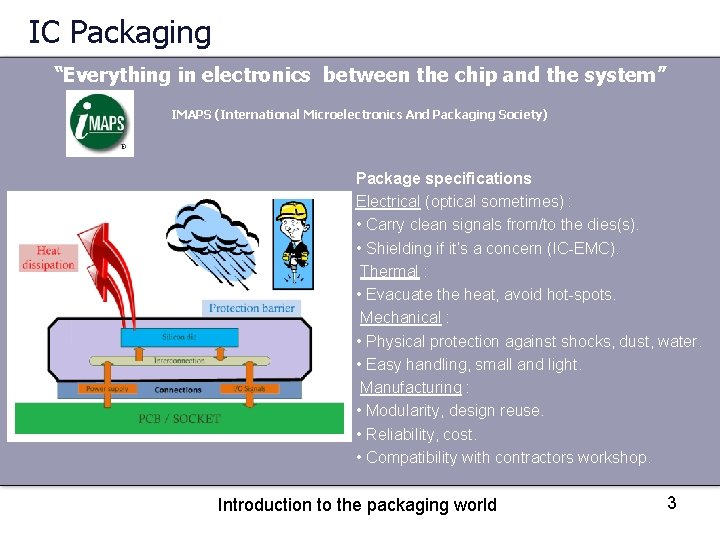
IC Packaging “Everything in electronics between the chip and the system” IMAPS (International Microelectronics And Packaging Society) Package specifications Electrical (optical sometimes) : • Carry clean signals from/to the dies(s). • Shielding if it’s a concern (IC-EMC). Thermal : • Evacuate the heat, avoid hot-spots. Mechanical : • Physical protection against shocks, dust, water. • Easy handling, small and light. Manufacturing : • Modularity, design reuse. • Reliability, cost. • Compatibility with contractors workshop. Introduction to the packaging world 3

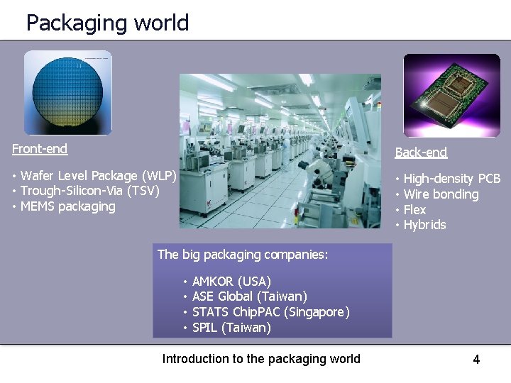
Packaging world Front-end Back-end • Wafer Level Package (WLP) • Trough-Silicon-Via (TSV) • MEMS packaging • High-density PCB • Wire bonding • Flex • Hybrids The big packaging companies: • AMKOR (USA) • ASE Global (Taiwan) • STATS Chip. PAC (Singapore) • SPIL (Taiwan) Introduction to the packaging world 4

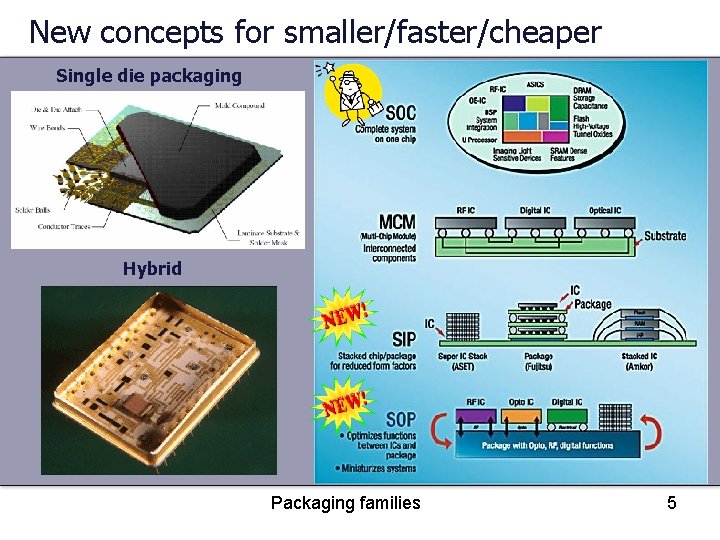
New concepts for smaller/faster/cheaper Single die packaging Hybrid Packaging families 5

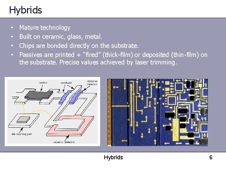
Hybrids • • Mature technology Built on ceramic, glass, metal. Chips are bonded directly on the substrate. Passives are printed + “fired” (thick-film) or deposited (thin-film) on the substrate. Precise values achieved by laser trimming. Hybrids 6

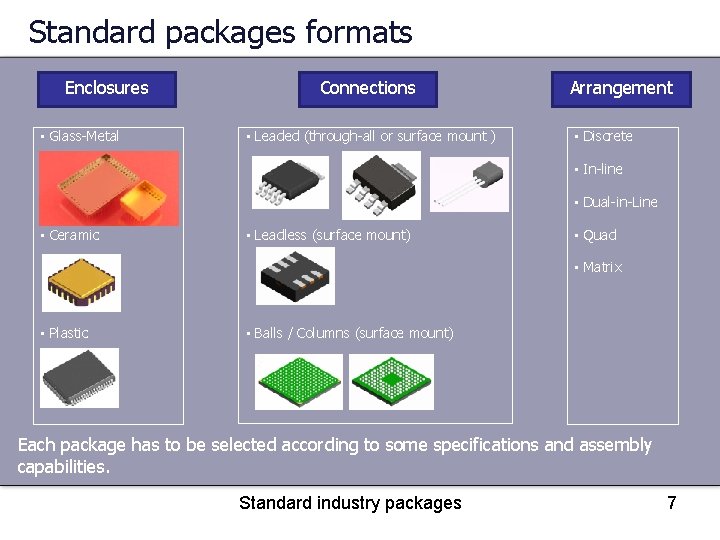
Standard packages formats Enclosures • Glass-Metal Connections • Leaded (through-all or surface mount ) Arrangement • Discrete • In-line • Dual-in-Line • Ceramic • Leadless (surface mount) • Quad • Matrix • Plastic • Balls / Columns (surface mount) Each package has to be selected according to some specifications and assembly capabilities. Standard industry packages 7

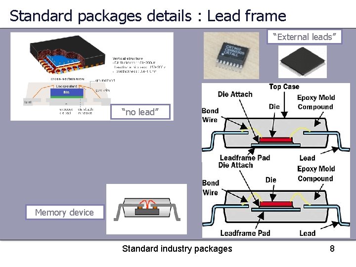
Standard packages details : Lead frame “External leads” “no lead” Memory device Standard industry packages 8

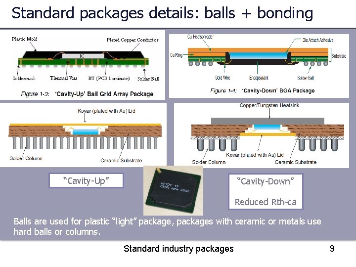
Standard packages details: balls + bonding “Cavity-Up” “Cavity-Down” Reduced Rth-ca Balls are used for plastic “light” package, packages with ceramic or metals use hard balls or columns. Standard industry packages 9

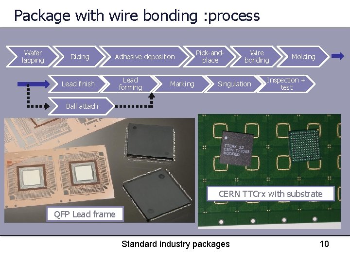
Package with wire bonding : process Wafer lapping Dicing Adhesive deposition Lead finish Lead forming Marking Pick-andplace Wire bonding Singulation Molding Inspection + test Ball attach CERN TTCrx with substrate QFP Lead frame Standard industry packages 10

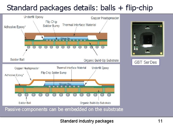
Standard packages details: balls + flip-chip GBT Ser. Des Passive components can be embedded on the substrate Standard industry packages 11

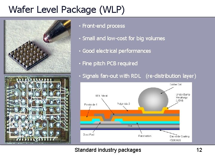
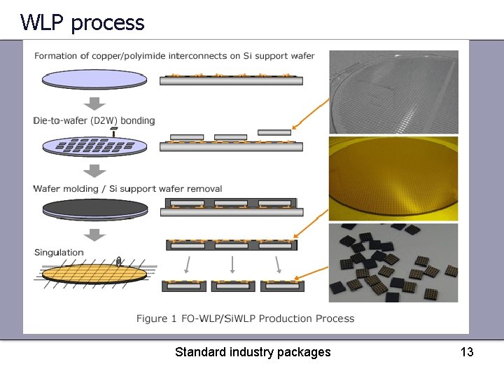
Wafer Level Package (WLP) • Front-end process • Small and low-cost for big volumes • Good electrical performances • Fine pitch PCB required • Signals fan-out with RDL (re-distribution layer) Standard industry packages 12

WLP process Standard industry packages 13

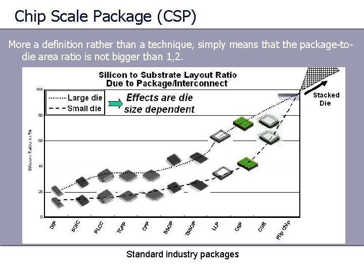
Chip Scale Package (CSP) More a definition rather than a technique, simply means that the package-todie area ratio is not bigger than 1, 2. Standard industry packages

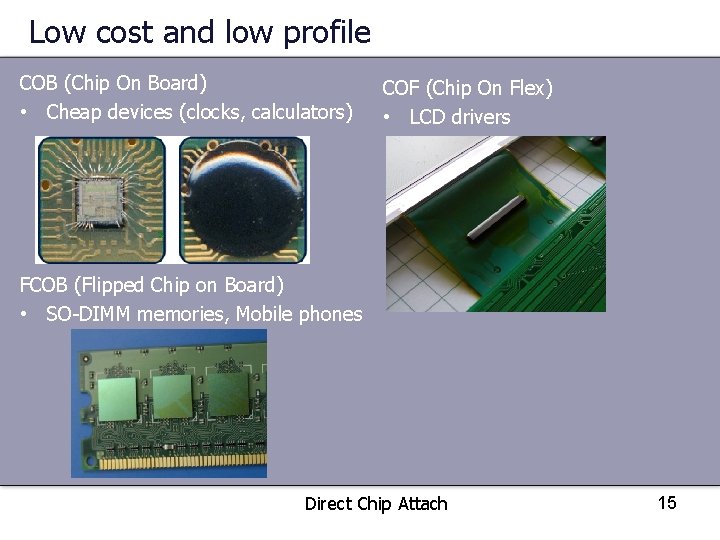
Low cost and low profile COB (Chip On Board) • Cheap devices (clocks, calculators) COF (Chip On Flex) • LCD drivers FCOB (Flipped Chip on Board) • SO-DIMM memories, Mobile phones Direct Chip Attach 15

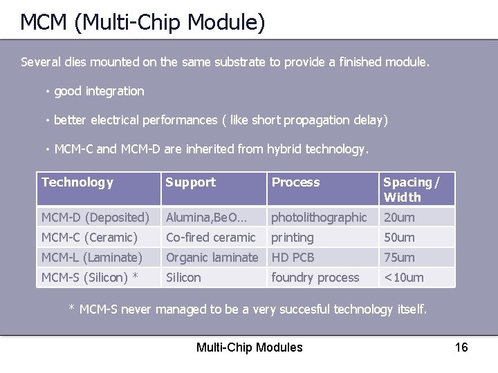
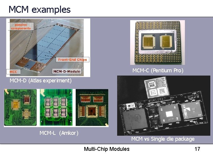
MCM (Multi-Chip Module) Several dies mounted on the same substrate to provide a finished module. • good integration • better electrical performances ( like short propagation delay) • MCM-C and MCM-D are inherited from hybrid technology. Technology Support Process Spacing/ Width MCM-D (Deposited) Alumina, Be. O… photolithographic 20 um MCM-C (Ceramic) Co-fired ceramic printing 50 um MCM-L (Laminate) Organic laminate HD PCB 75 um MCM-S (Silicon) * Silicon foundry process <10 um * MCM-S never managed to be a very succesful technology itself. Multi-Chip Modules 16

MCM examples MCM-C (Pentium Pro) MCM-D (Atlas experiment) MCM-L (Amkor) MCM vs Single die package Multi-Chip Modules 17

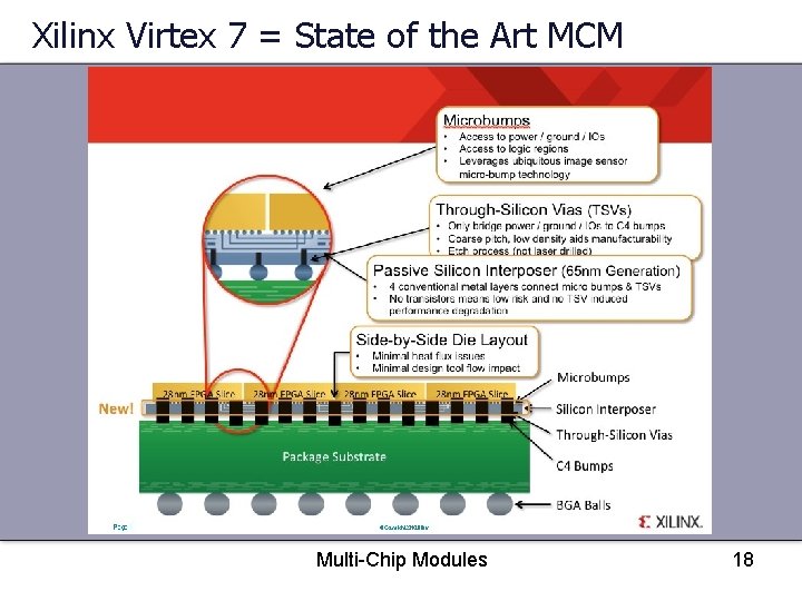
Xilinx Virtex 7 = State of the Art MCM Multi-Chip Modules 18

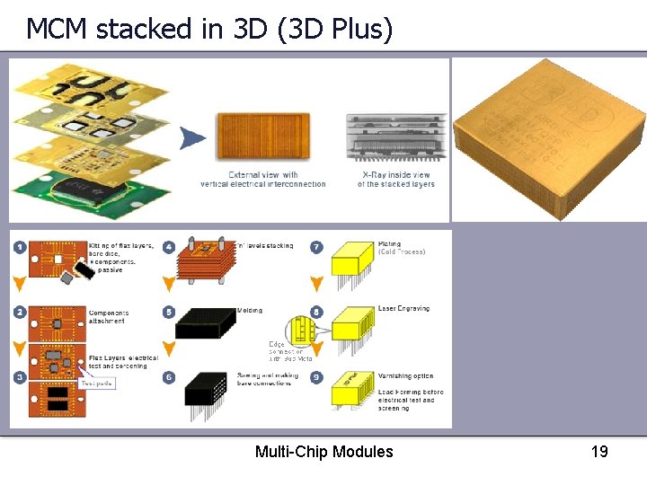
MCM stacked in 3 D (3 D Plus) Multi-Chip Modules 19

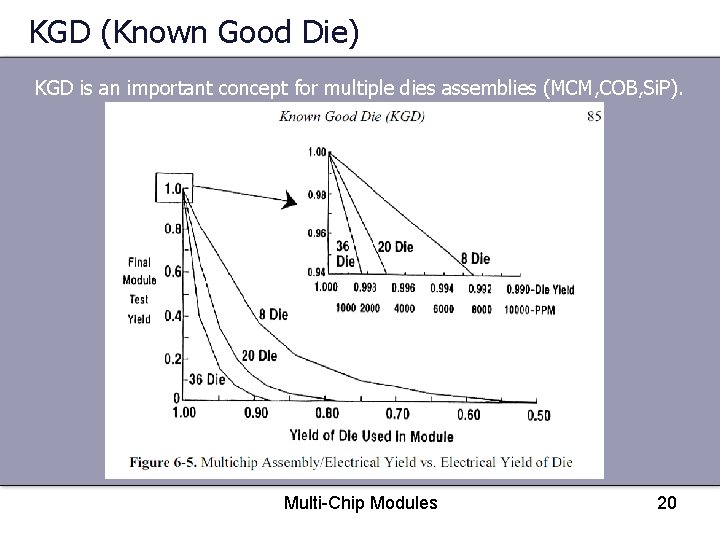
KGD (Known Good Die) KGD is an important concept for multiple dies assemblies (MCM, COB, Si. P). Multi-Chip Modules 20

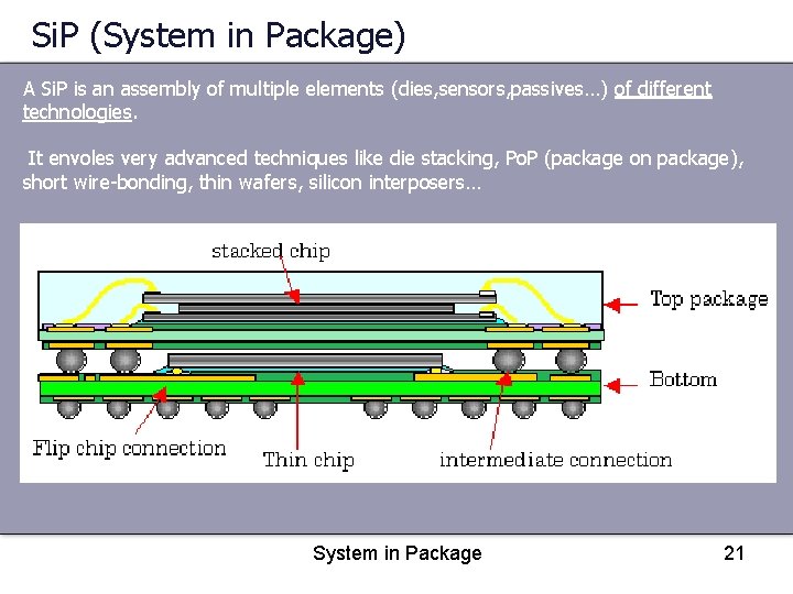
Si. P (System in Package) A Si. P is an assembly of multiple elements (dies, sensors, passives…) of different technologies. It envoles very advanced techniques like die stacking, Po. P (package on package), short wire-bonding, thin wafers, silicon interposers… System in Package 21

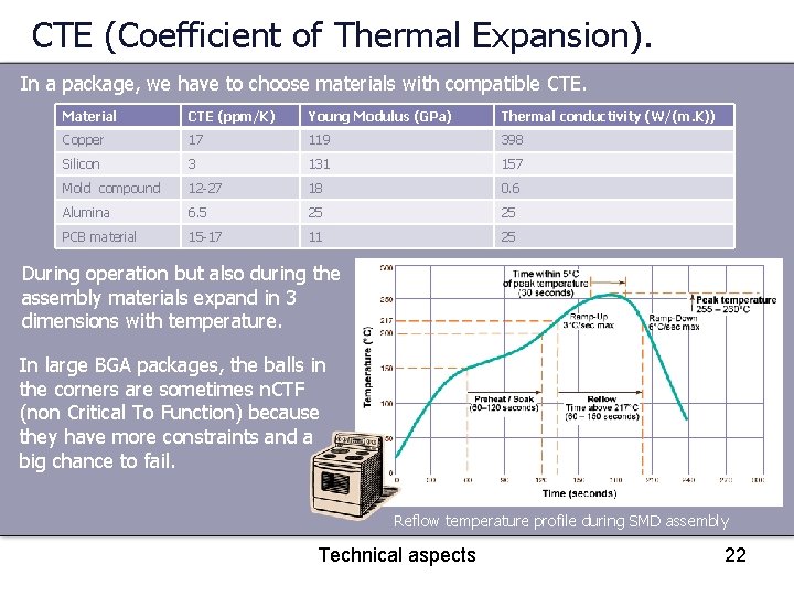
CTE (Coefficient of Thermal Expansion). In a package, we have to choose materials with compatible CTE. Material CTE (ppm/K) Young Modulus (GPa) Thermal conductivity (W/(m. K)) Copper 17 119 398 Silicon 3 131 157 Mold compound 12 -27 18 0. 6 Alumina 6. 5 25 25 PCB material 15 -17 11 25 During operation but also during the assembly materials expand in 3 dimensions with temperature. In large BGA packages, the balls in the corners are sometimes n. CTF (non Critical To Function) because they have more constraints and a big chance to fail. Reflow temperature profile during SMD assembly Technical aspects 22

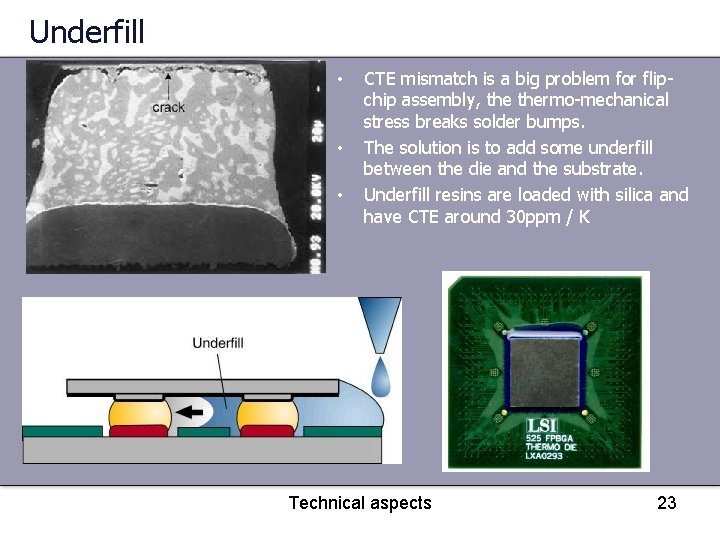
Underfill • • • CTE mismatch is a big problem for flipchip assembly, thermo-mechanical stress breaks solder bumps. The solution is to add some underfill between the die and the substrate. Underfill resins are loaded with silica and have CTE around 30 ppm / K Technical aspects 23

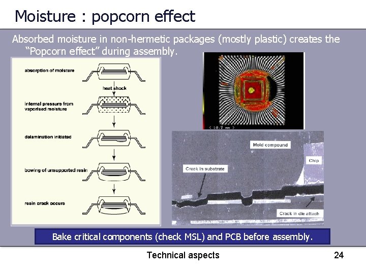
Moisture : popcorn effect Absorbed moisture in non-hermetic packages (mostly plastic) creates the “Popcorn effect” during assembly. Bake critical components (check MSL) and PCB before assembly. Technical aspects 24

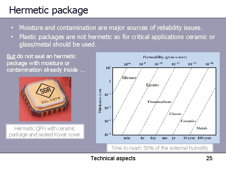
Hermetic package • Moisture and contamination are major sources of reliability issues. • Plastic packages are not hermetic so for critical applications ceramic or glass/metal should be used. But do not seal an hermetic package with moisture or contamination already inside … Hermetic QFN with ceramic package and sealed Kovar cover Time to reach 50% of the external humidity Technical aspects 25

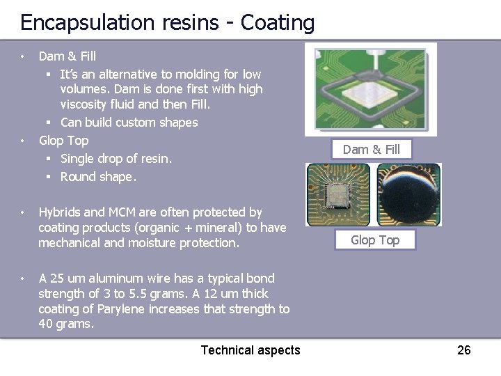
Encapsulation resins - Coating • • Dam & Fill § It’s an alternative to molding for low volumes. Dam is done first with high viscosity fluid and then Fill. § Can build custom shapes Glop Top § Single drop of resin. § Round shape. Hybrids and MCM are often protected by coating products (organic + mineral) to have mechanical and moisture protection. Dam & Fill Glop Top A 25 um aluminum wire has a typical bond strength of 3 to 5. 5 grams. A 12 um thick coating of Parylene increases that strength to 40 grams. Technical aspects 26

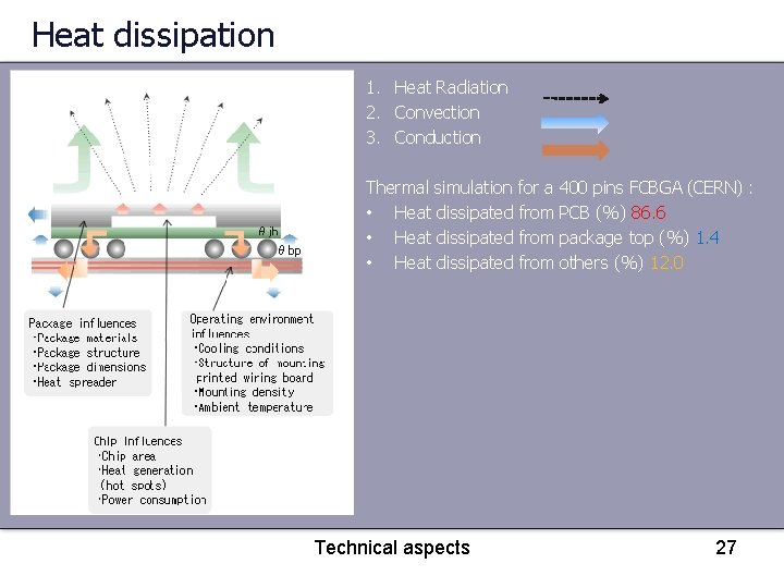
Heat dissipation 1. Heat Radiation 2. Convection 3. Conduction Thermal simulation for a 400 pins FCBGA (CERN) : • Heat dissipated from PCB (%) 86. 6 • Heat dissipated from package top (%) 1. 4 • Heat dissipated from others (%) 12. 0 Technical aspects 27

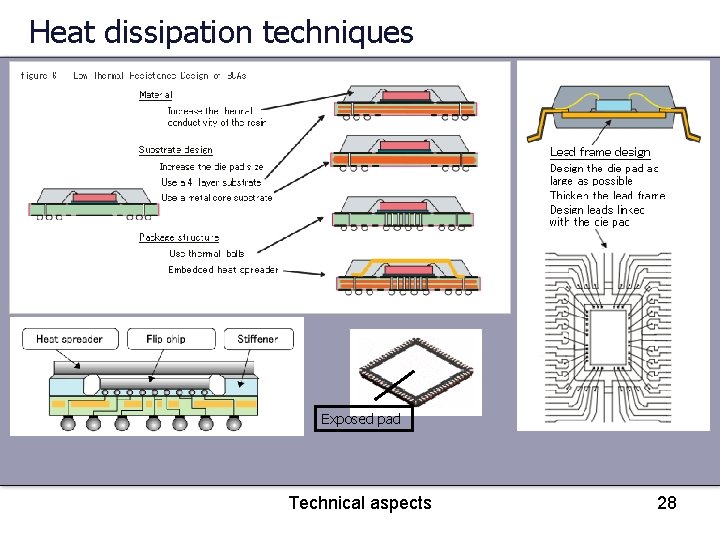
Heat dissipation techniques Exposed pad Technical aspects 28

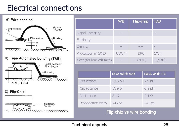
Electrical connections WB Flip-chip Signal Integrity --- - -- Flexibilty + -- - Density + ++ - 85% ? 13% + - (NRE) Production in 2010 Cost (for low volumes) TAB 2% ? - (NRE) PGA with WB BGA with FC Inductance 19. 6 n. H 7. 9 n. H Capacitance 15. 9 p. F 6. 2 p. F Resistance 21 Ω 2. 1 Ω Propagation delay 946 ps 243 ps Flip-chip vs wire bonding Technical aspects 29

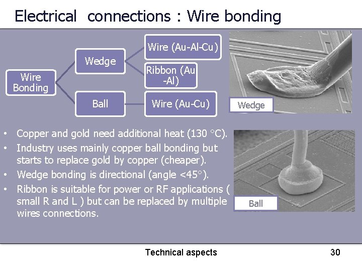
Electrical connections : Wire bonding Wire (Au-Al-Cu) Wedge Wire Bonding Ball Ribbon (Au -Al) Wire (Au-Cu) • Copper and gold need additional heat (130 °C). • Industry uses mainly copper ball bonding but starts to replace gold by copper (cheaper). • Wedge bonding is directional (angle <45°). • Ribbon is suitable for power or RF applications ( small R and L ) but can be replaced by multiple wires connections. Technical aspects Wedge Ball 30

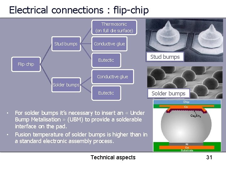
Electrical connections : flip-chip Thermosonic (on full die surface) Stud bumps Conductive glue Eutectic Flip chip Stud bumps Conductive glue Solder bumps Eutectic • • Solder bumps For solder bumps it’s necessary to insert an « Under Bump Metalisation » (UBM) to provide a solderable interface on the pad. Fusion temperature of solder bumps is higher than in a standard electronic assembly process. Technical aspects 31

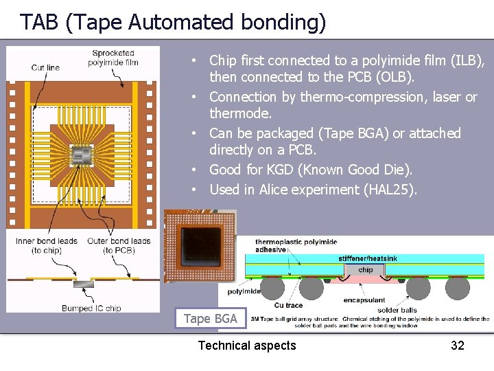
TAB (Tape Automated bonding) • Chip first connected to a polyimide film (ILB), then connected to the PCB (OLB). • Connection by thermo-compression, laser or thermode. • Can be packaged (Tape BGA) or attached directly on a PCB. • Good for KGD (Known Good Die). • Used in Alice experiment (HAL 25). Tape BGA Technical aspects 32

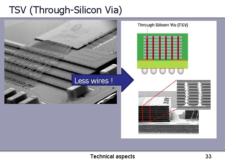
TSV (Through-Silicon Via) Less wires ! Technical aspects 33

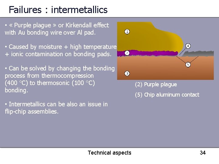
Failures : intermetallics • « Purple plague » or Kirkendall effect with Au bonding wire over Al pad. • Caused by moisture + high temperature + ionic contamination on bonding pads. • Can be solved by changing the bonding process from thermocompression (400 °C) to thermosonic (100 °C) bonding. (2) Purple plague (5) Chip aluminum contact • Intermetallics can be also an issue in flip-chip assemblies. Technical aspects 34

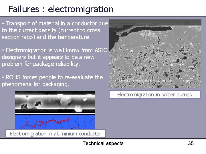
Failures : electromigration • Transport of material in a conductor due to the current density (current to cross section ratio) and the temperature. • Electromigration is well know from ASIC designers but it appears to be a new problem for package reliability. • ROHS forces people to re-evaluate the phenomena for packaging. Electromigration in solder bumps Electromigration in aluminium conductor Technical aspects 35

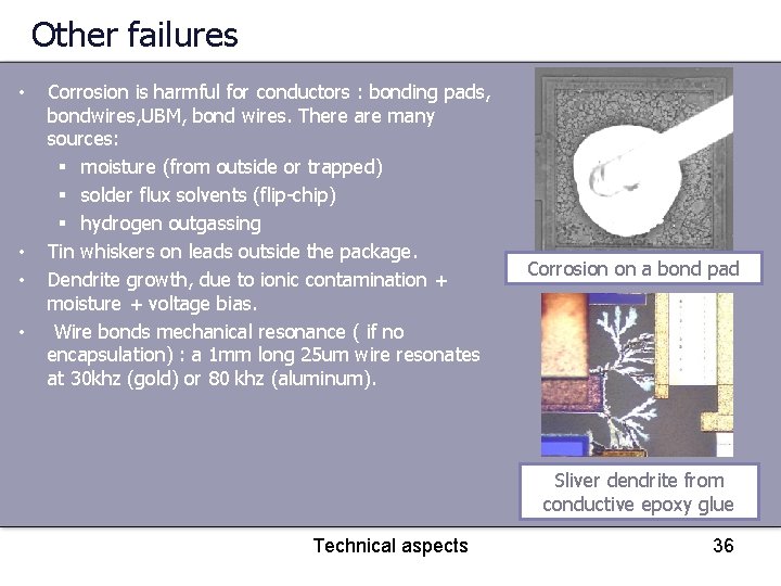
Other failures • • Corrosion is harmful for conductors : bonding pads, bondwires, UBM, bond wires. There are many sources: § moisture (from outside or trapped) § solder flux solvents (flip-chip) § hydrogen outgassing Tin whiskers on leads outside the package. Dendrite growth, due to ionic contamination + moisture + voltage bias. Wire bonds mechanical resonance ( if no encapsulation) : a 1 mm long 25 um wire resonates at 30 khz (gold) or 80 khz (aluminum). Corrosion on a bond pad Sliver dendrite from conductive epoxy glue Technical aspects 36

Conclusion • IC packaging is a mixed of many disciplines : materials science, mechanical and chemical engineering and almost no electronic. • Reliability is a very important parameter, mainly based on experience. • Embedded electronic and MEMS forced packaging engineers to innovate a lot but it’s still a bottleneck. R&D is focused now on 3 D packaging and cooling. Short bibliography: • • • “Integrated Circuit Packaging, Assembly and Interconnections” - William J. Greig “Wire Bonding in Microelectronics 3 rd edition” - George Harman “ Miniaturisation MCM & Packaging en Electronique et micro-electronique” – Alexandre Val