
Integrated Circuits for the INO Praveen Kumar Harshit
- Slides: 23
Integrated Circuits for the INO Praveen Kumar Harshit Vaishnav Nagendra Krishnapura Indian Institute of Technology, Madras 13 th February 2012
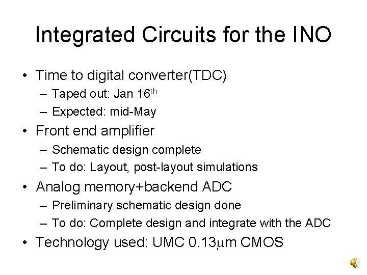
Integrated Circuits for the INO • Time to digital converter(TDC) – Taped out: Jan 16 th – Expected: mid-May • Front end amplifier – Schematic design complete – To do: Layout, post-layout simulations • Analog memory+backend ADC – Preliminary schematic design done – To do: Complete design and integrate with the ADC • Technology used: UMC 0. 13 mm CMOS
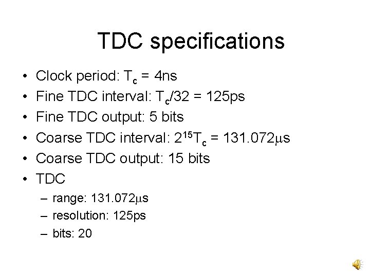
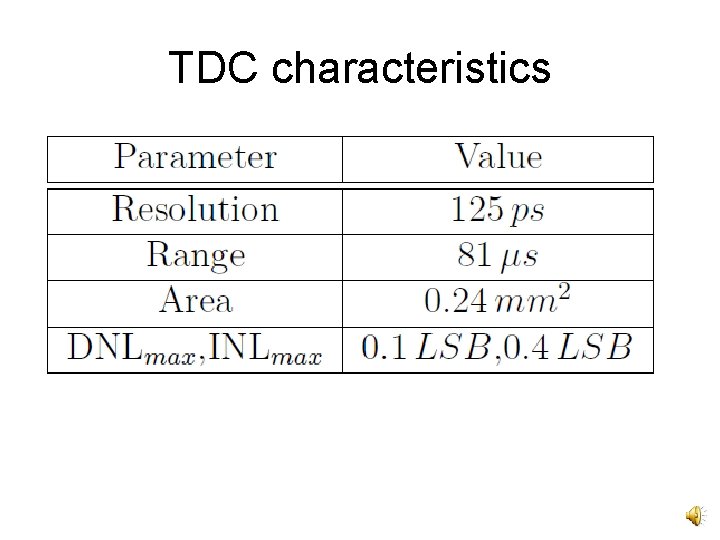
TDC specifications • • • Clock period: Tc = 4 ns Fine TDC interval: Tc/32 = 125 ps Fine TDC output: 5 bits Coarse TDC interval: 215 Tc = 131. 072 ms Coarse TDC output: 15 bits TDC – range: 131. 072 ms – resolution: 125 ps – bits: 20
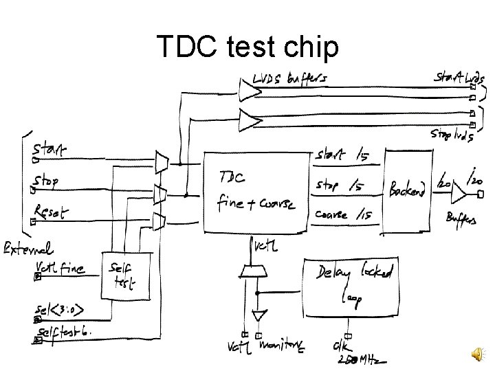
TDC test chip
TDC test chip • • Currently a single-hit TDC Needs reset before next count Can be adapted to multi-hit 20 bit parallel output
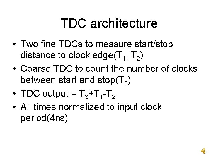
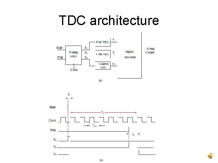
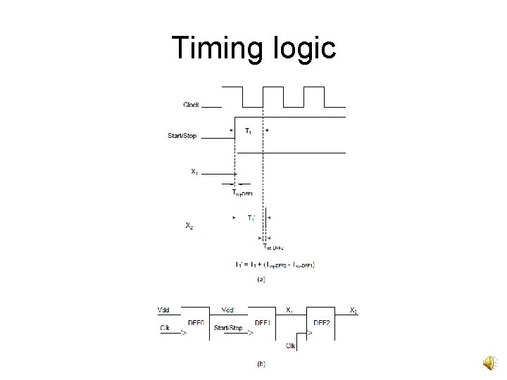
TDC architecture • Two fine TDCs to measure start/stop distance to clock edge(T 1, T 2) • Coarse TDC to count the number of clocks between start and stop(T 3) • TDC output = T 3+T 1 -T 2 • All times normalized to input clock period(4 ns)
TDC architecture
Flash TDC
Voltage controlled delay cell
Timing logic
D flip flop with reduced setup time
Coarse TDC, backend • Coarse TDC: Synthesized 15 bit counter • Backend: Synthesized arithmetic circuit to compute T 3+T 1 -T 2
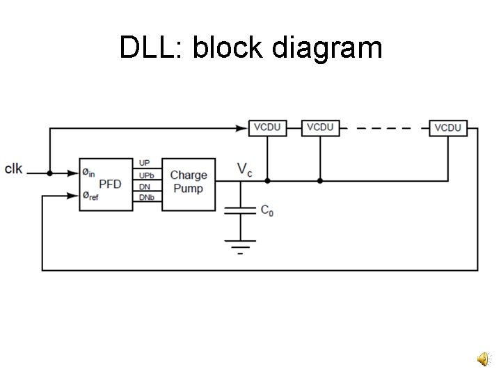
DLL: block diagram
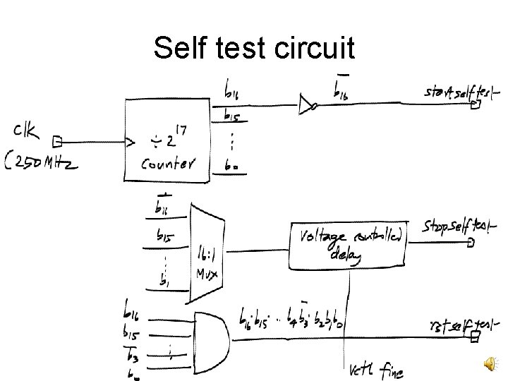
Self test circuit
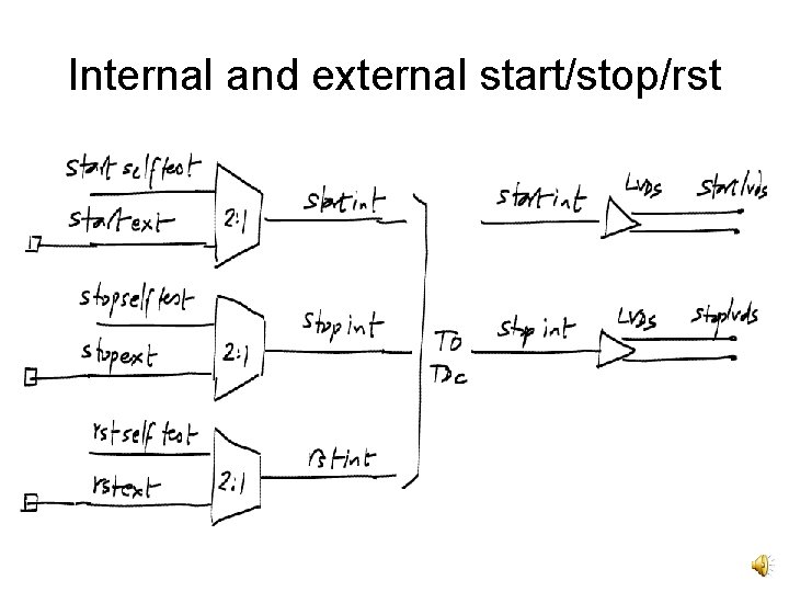
Internal and external start/stop/rst
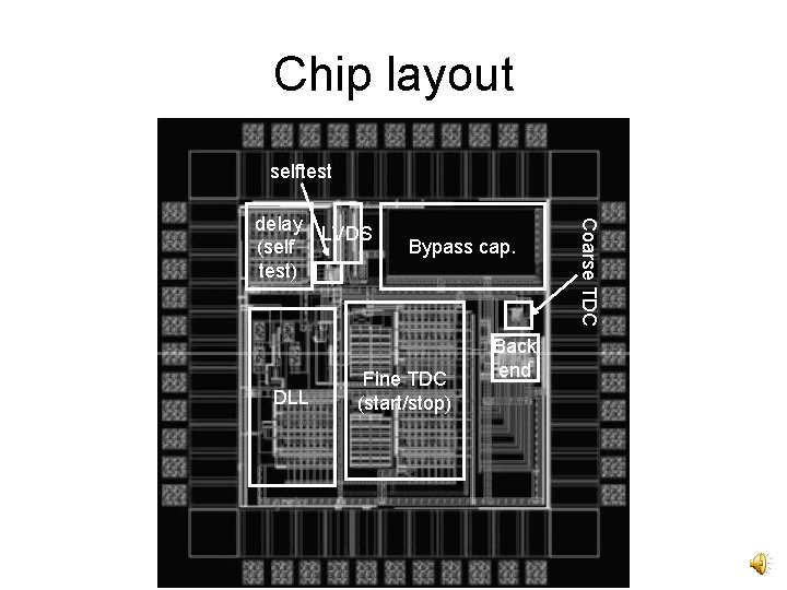
Chip layout selftest DLL Bypass cap. Fine TDC (start/stop) Back end Coarse TDC delay LVDS (self test)
DLL delay nonlinearity
DLL locking
DLL characteristics
TDC: simulated characteristics
TDC characteristics
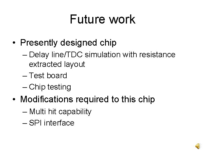
Future work • Presently designed chip – Delay line/TDC simulation with resistance extracted layout – Test board – Chip testing • Modifications required to this chip – Multi hit capability – SPI interface
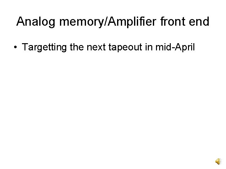
Analog memory/Amplifier front end • Targetting the next tapeout in mid-April