Integrated Circuit Structure Course Objectives The main objective

Integrated Circuit Structure

Course Objectives The main objective of this course is to Describe the characteristics of Op-Amp and its internal structure. Explain implementation of linear and nonlinear applications of Op-amp. Introduce special purpose IC’s such as PLL, Converters and their applications. Teach designing of active filters and oscillators using operational amplifiers. Course Outcomes After successfully completing the course students will be able to: Explain internal structure and characteristics of Op-Amp. Determine various performance parameters of op-amp and Explain their significance. Analyze and Implement linear and nonlinear applications of Op-Amp. Design converters, Oscillators and filters using Op-amp. Explain and Apply functionalities of PLL. To Improve written, oral, and presentation skills related to Integrated Circuits and engage in life-long learning.

Syllabus
 is a device")
What is an Op-Amp? An Operational Amplifier (known as an “Op-Amp”) is a device that is used to amplify a signal using an external power source Op-AMP is a very high gain amplifier fabricated on Integrated Circuit (IC) Op-Amps are generally composed of: Transistors, Resistors, Capacitors = + + We recognize an Op-Amp as a mass-produced component found in countless electronics What an Op-Amp looks like to a layperson What an Op-Amp looks like to an engineer

Operational Amplifier There are 8 pins in a common Op-Amp, like the 741 which is used in many instructional courses. For simplicity, an Op-Amp is often depicted as this:
")
Opamp and its maths The difference between the two inputs voltages (V+ and V-) multiplied by the gain (A, “amplification factor”) of the Op-Amp gives you the output voltage A = Vout /(V+ – V-) or A = Vout /Vin The above expression can be interpreted as Vout = A (V+ - V-) The output voltage can only be as high as the difference between the power supply (Vs+ / Vs-)and ground (0 Volts) i. e The maximum output is the power supply voltage

OPAMP terminals If input is applied to non inverting input terminal, then output will be in-phase with input If input is applied to inverting input terminal, then output will be 180 degrees out of phase with input If inputs are applied to both terminals, then output will be proportional to difference between the two inputs

The output voltage never excess the DC voltage supply of the Op-Amp

Applications of Op-Amps Filters Types: • Low pass filter • High pass filter • Band pass filter • Cascading (2 or more filters connected together) Low pass filter C R 2 R 1 + - + + Vcc - Vcc + V 0 __
 Amplification Need to measure difference in voltage from lead")
Applications of Op-Amps Electrocardiogram (EKG) Amplification Need to measure difference in voltage from lead 1 and lead 2 60 Hz interference from electrical equipment

Applications of Op-Amps Simple EKG circuit Uses differential amplifier to cancel common mode signal and amplify differential mode signal Realistic EKG circuit Uses two non-inverting amplifiers to first amplify voltage from each lead, followed by differential amplifier Forms an “instrumentation amplifier”

Transfer Characteristics of Opamp Saturation is caused by increasing/decreasing the input voltage to cause the output voltage to equal the power supply’s voltage* As mentioned earlier, the maximum output value is the supply voltage, positive and negative. The gain (A) is the slope between saturation points. The slope is normally much steeper than it is shown here. Potentially just a few milli-volts (m. V) of change in the difference between V+ and V- could cause the op-amp to reach the saturation level * Note that saturation level of traditional Op-Amp is 80% of supply voltage with exception of CMOS opamp which has a saturation at the power supply’s voltage

Internal Block Diagram Non-Inverting Input Differential Amplifier Stage Intermediate Stage Level Shifter Stage Output Stage Dual Input Balanced output differential Amplifier Dual Input Unbalanced output differential Amplifier Level Shifter Emitter follower using constant current biasing Push Pull Amplifier Four stages can be identified – Ø Input stage or differential amplifier stage can amplify difference between two input signals; Input resistance is very high; Draws zero current from the input sources Ø Intermediate stage (or stages) use direct coupling; provide very high gain Ø Level shifter stage shifts the dc level of output voltage to zero (can be adjusted manually using two additional terminals) Ø Output stage is a power amplifier stage; has very small output resistance; so output voltage is the same, no matter what is the value of load resistance connected to the output terminal Ø Op-amp is a high gain amplifier usable from 0 to 1 MHz

741 Op-Amp Internal Schematic current mirror output stage voltage level shifter differential amplifier current mirror high-gain amplifier

Differential Amplifier Configurations 1. 2. 3. 4. Dual Input balanced output differential amplifier Dual Input unbalanced output differential amplifier Single input unbalanced output differential amplifier Dual Input, Balanced Output Difference Amplifier: DC Analysis

Dual Input, Balanced Output Difference Amplifier: AC Analysis AC equivalent circuit using r parameter
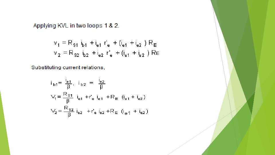


Differential Input Resistance:

Output Resistance: RO 1 = RO 2 = RC Ø Example - 1 Ø The following specifications are given for the dual input, balanced-output differential amplifier of fig. 1: RC = 2. 2 kΩ, RB = 4. 7 kΩ, Rin 1 = Rin 2 = 50 Ω , +VCC = 10 V, -VEE = -10 V, βdc =100 and VBE = 0. 715 V. Determine the operating points (ICQ and VCEQ) of the two transistors. Ø Example - 2 Ø For the dual input, balanced output differential amplifier of Example-1: Ø Determine the output voltage (vo) if vin 1 = 50 m. V peak to peak (pp) at 1 k. Hz and vin 2 = 20 m. V pp at 1 k. Hz. Ø What is the maximum peal to peak output voltage without clipping?

Constant Current Biasing In the dc analysis of differential amplifier, we have seen that the emitter current I E depends upon the value of bdc. To make operating point stable IE current should be constant irrespective value of bdc. For constant IE, RE should be very large. This also increases the value of CMRR but if RE value is increased to very large value, IE (quiescent operating current) decreases. To maintain same value of IE, the emitter supply VEE must be increased. To get very high value of resistance RE and constant IE, current bias is used.
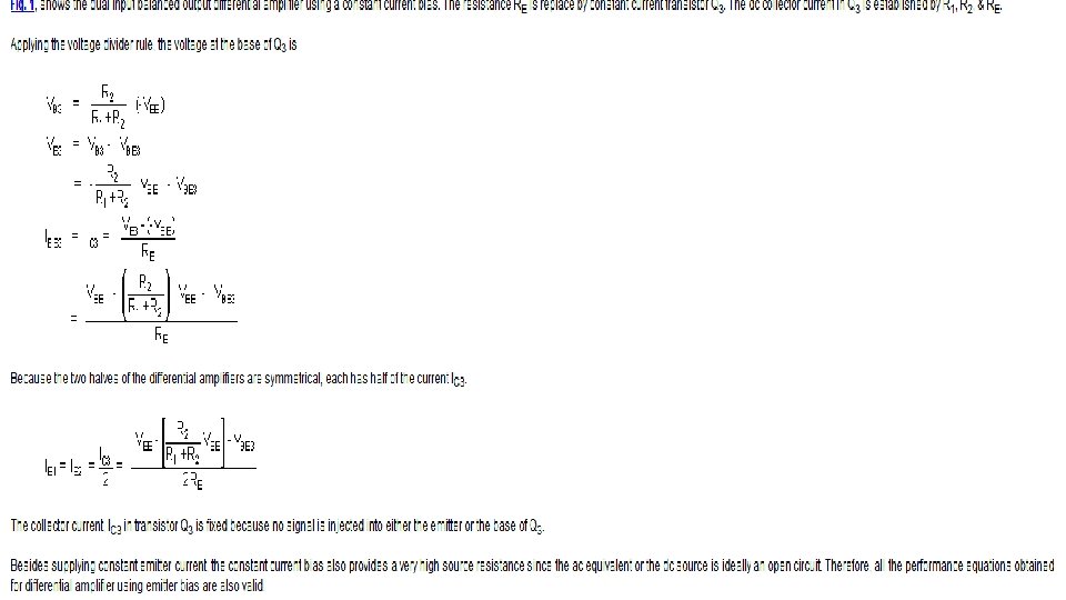


Current Mirror The circuit in which the output current is forced to equal the input current is said to be a current mirror circuit. Thus in a current mirror circuit, the output current is a mirror image of the input current. The current mirror circuit is shown in Since Q 3 and Q 4 are identical transistors the current and voltage are approximately same

Level Shifter


- Slides: 30