Integrated Circuit Processing Pulling ingots Wafers Patterning Fabrication
Integrated Circuit Processing · · · · Pulling ingots Wafers Patterning Fabrication cycle Testing Packaging CAD design of ICs Future issues (5. 1)
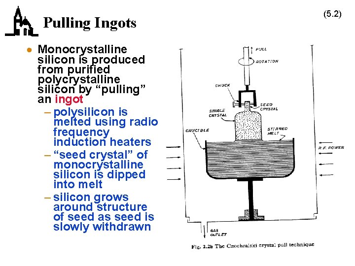
Pulling Ingots · Monocrystalline silicon is produced from purified polycrystalline silicon by “pulling” an ingot – polysilicon is melted using radio frequency induction heaters – “seed crystal” of monocrystalline silicon is dipped into melt – silicon grows around structure of seed as seed is slowly withdrawn (5. 2)
Pulling Ingots (continued) · Produces an ingot of pure silicon – 400 mm - 1000 mm long (15” - 39”) – 150 mm - 200 mm in diameter (6” - 8”) · Growth is a slow process – 10 - 20 hours · Silicon is often doped as it’s grown (5. 3)
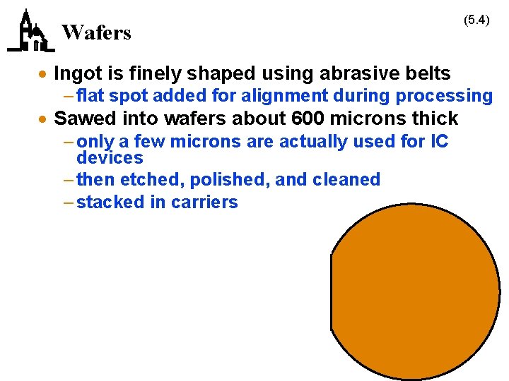
Wafers (5. 4) · Ingot is finely shaped using abrasive belts – flat spot added for alignment during processing · Sawed into wafers about 600 microns thick – only a few microns are actually used for IC devices – then etched, polished, and cleaned – stacked in carriers
Silicon Dioxide and Polysilicon (5. 5) · Silicon dioxide is created by interaction between silicon and oxygen or water vapor – Si + O 2 = Si. O 2 or Si + 2 H 2 O = Si. O 2 + 2 H 2 – protects surface from contaminants – forms insulating layer between conductors – form barrier to dopants during diffusion or ion implantation 40% – grows above and into silicon surface · Polysilicon – silicon without a single crystal structure – created when silicon is epitaxially grown on Si. O 2 – also a conductor, but with much more resistance than metal or diffused layers – commonly used (heavily doped) for gate connections in most MOS processes 60%
Patterning (5. 6) · Patterning creates a regular pattern on the surface of the chip, which is used to create features of the IC – involves alternative lithography and etching steps – each of several layers involves a separate pattern · Lithography – patterns are contained on masks » eg, chrome on glass – surface of the wafer is covered with photoresist » organic material sensistive to uv light or X-rays » spin and bake » positive resist becomes more soluable when exposed • resist will be removed where mask is clear » negative resist becomes less soluable when exposed • resist will be removed where mask is opaque
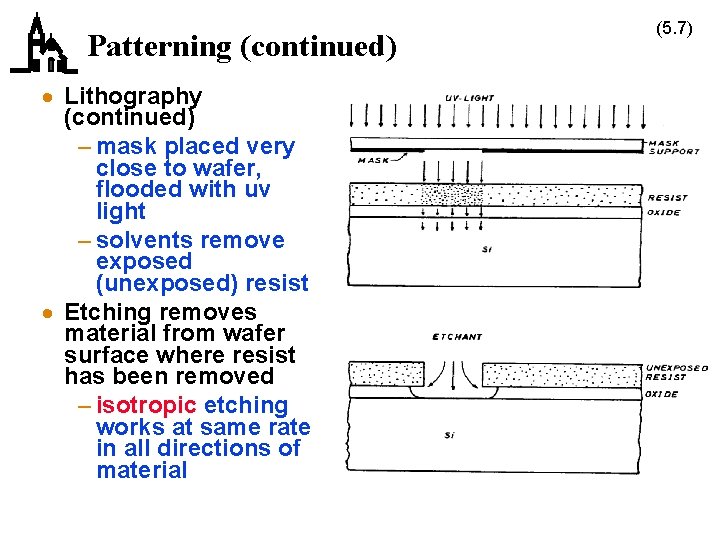
Patterning (continued) · Lithography (continued) – mask placed very close to wafer, flooded with uv light – solvents remove exposed (unexposed) resist · Etching removes material from wafer surface where resist has been removed – isotropic etching works at same rate in all directions of material (5. 7)
Patterning (continued) (5. 8) · Etching (continued) – anisotropic etching works faster in one direction than the other – wet etching uses liquid solvents to remove materials » eg, HF for Si. O 2 – dry etching uses gas to remove materials » less undercutting » can monitor reactants during process, determine automatically when etching is finished · Finally, remaining photoresist is removed – organic solvents or chromic acid – pure oxygen, to oxidize organic resist materials
Metalization (5. 9) · Metalization is used to create contacts with the silicon and to make interconnections on the chip · Desired properties are – low resistivity » in ohms/square – good adhesion to silicon and insulators – good coverage of steps in chip surface – immunity to corrosion – ductility (so temperature cycles don’t cause failures)
Metalization (continued) (5. 10) · Aluminum is common choice but – Al causes spikes into Si, giving leaky junctions – high currents carry Al atoms with them, creating shorts – low melting point prohibits high heat processing later · Latest step is to use copper – IBM has been shipping chips with copper for a year » smaller, 50% less power consumption – other fabs to follow soon
NMOS Fabrication Cycle · Start with p-type silicon wafer · Grow a “passivation” layer of Si. O 2 (silicon dioxide) over the entire wafer · Use lithography and a mask to define the source and drain areas, and etch to expose the wafer surface – first masking step · Diffuse phosphorous to create source and drain n-type regions (5. 11)
NMOS Fabrication Cycle (continued) (5. 12) · Use lithography and a mask to define the gate area, and etch to expose the wafer surface – second masking step · Grow a thin layer of Si. O 2 as the gate insulator · Use lithography and a mask to define the source and drain contact areas, and etch to expose the wafer surface – third masking step
NMOS Fabrication Cycle (continued) (5. 13) · Evaporate metal (typically copper) over entire surface of wafer · Use lithography and a mask to define the interconnect areas, and etch away all other metal – fourth masking step An excellent animation of this process is available at http: //jas. eng. buffalo. edu/applets/ education/fab/NMOS/nmos. html
Testing · Two different kinds of testing – process testing – function testing · Process testing uses special patterns in separate areas on the wafer to measure important parameters – resistivity of various conductive materials » diffused or ion implanted areas » polysilicon » metal – contact resistance – line width and mask alignment – simple components » transistors » capacitors » simple logic gates (5. 14)
Testing (continued) · Functional testing – simple or regular circuits can be tested completely » memories – complex circuits cannot be fully tested » test individual functions or paths • registers • arithmetic and logic units • simple instructions • data paths – modifying designs for easier testing, and automated visual inspection for particular flaws, are active research areas (5. 15)
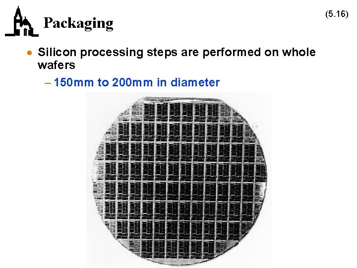
Packaging · Silicon processing steps are performed on whole wafers – 150 mm to 200 mm in diameter (5. 16)
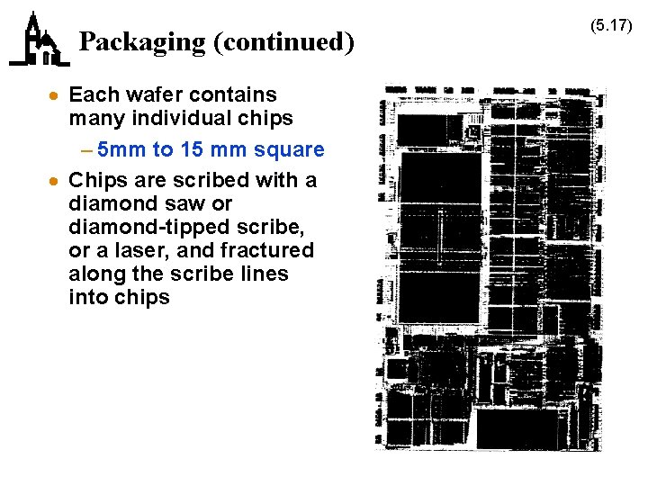
Packaging (continued) · Each wafer contains many individual chips – 5 mm to 15 mm square · Chips are scribed with a diamond saw or diamond-tipped scribe, or a laser, and fractured along the scribe lines into chips (5. 17)
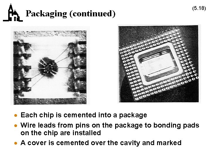
Packaging (continued) (5. 18) · Each chip is cemented into a package · Wire leads from pins on the package to bonding pads on the chip are installed · A cover is cemented over the cavity and marked
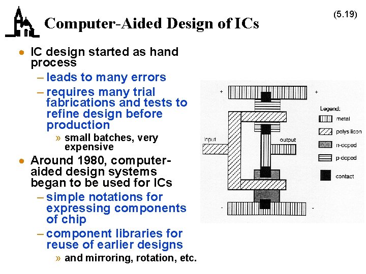
Computer-Aided Design of ICs · IC design started as hand process – leads to many errors – requires many trial fabrications and tests to refine design before production » small batches, very expensive · Around 1980, computeraided design systems began to be used for ICs – simple notations for expressing components of chip – component libraries for reuse of earlier designs » and mirroring, rotation, etc. (5. 19)
(5. 20) Computer-Aided Design of ICs (continued) · CAD systems (continued) – enforce design rules – help with routing of connections – simulation of interim designs » 2 -D or 3 -D device simulators » logic simulators » timing simulators · Design and layout happens at display · Simulation happens in batch mode – extremely computation intensive · Once design is ready for fabrication, CAD system produces pattern generation files
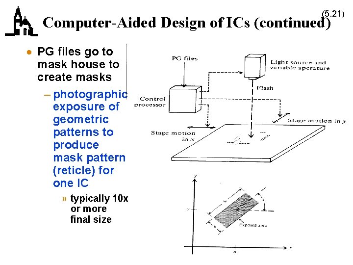
(5. 21) Computer-Aided Design of ICs (continued) · PG files go to mask house to create masks – photographic exposure of geometric patterns to produce mask pattern (reticle) for one IC » typically 10 x or more final size
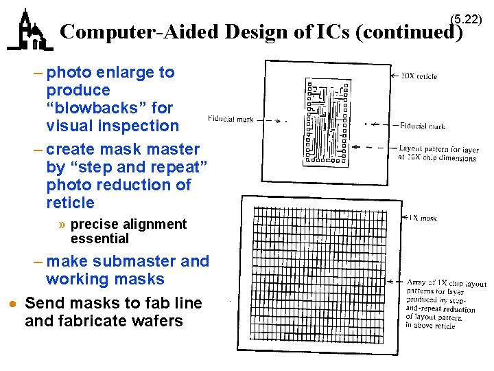
(5. 22) Computer-Aided Design of ICs (continued) – photo enlarge to produce “blowbacks” for visual inspection – create mask master by “step and repeat” photo reduction of reticle » precise alignment essential – make submaster and working masks · Send masks to fab line and fabricate wafers
IC Design Rules (5. 23) · Want design of IC to be independent of process used to implement design – especially want to scale as process technologies improve · Place constraints on widths, separations, overlaps – base all measures on elementary distance unit l – each process defines a value for l in microns – pattern generator produces output files appropriately · Examples – diffused regions >= 2 l – minimum line width 2 l – separation of lines >= l – gate overlap >= l · Current processes have l = 0. 18 - 0. 25 microns
Future Issues (5. 24) · Current state-of-the-art – 0. 18 micron feature size – die size about 2. 5 cm 2 – about 5. 5 million transistors on logic devices – 64 Mbit DRAMS » 64 million transistors · Lithography – wavelength of visible light is about 0. 5 microns » less than this difficult to pattern with visible light » but 0. 18 micron process is optical » uses phase coherence with laser light – electon beam exposure » expose resist directly on Si (no mask) – electron beam reticles, x-ray exposure of wafer » good for 0. 0? micron features » physical limit of Si
Future Issues (continued) · Die size – yield goes down as die size goes up – wafer scale integration – hampered by warping of wafer since Si and Si. O 2 expand contract at different rates · Vertical stacking · Testing – improved design for testability – automated visual inspection · Expense management – partnerships (5. 25)
- Slides: 25