Integrated Chip IC System Reliability Miniaturization Cost reduction
 System Reliability Miniaturization & Cost reduction Operating Speed Low Power Consumption")
Integrated Chip (IC) System Reliability Miniaturization & Cost reduction Operating Speed Low Power Consumption

Monolithic IC Technology • • Circuit from Single crystal. All components on single chip. Batch (mass/bulk) production – Reduced Cost. Inspite of many faults, large quantity due to batch size. 10 cm wafer can have 80000 chips. • As all processes on a single plane -> Planar Technique. • Size of chips range from 10 mm 2 to 350 mm 2. • Over 1 million chips in every 1 mm 2.

IC Fabrication by Planar Process - Steps Involved 1. 2. 3. 4. 5. 6. 7. 8. 9. Silicon Wafer (substrate) preparation Epitaxial Growth Oxidation Photolithography Diffusion Ion implantation Isolation Technique Metallization Assembly Processing & Packaging

STEP 1 SILICON WAFER PREPARATION

Basic Process Steps for Wafer Preparation Crystal Growth Wafer Lapping and Edge Grind Cleaning Shaping Etching Inspection Wafer Slicing Polishing Packaging
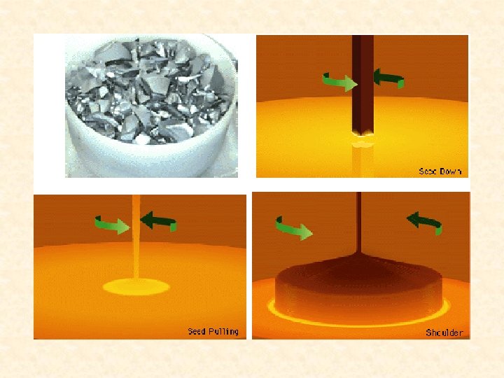
 Czochralski process: Ø Initial material 99. 9999% pure. Ø Silicon + Dopant heated")
a) Czochralski process: Ø Initial material 99. 9999% pure. Ø Silicon + Dopant heated to > 1420 C (melting point). Ø Single thin Silicon rod (cylinder) introduced into melt. Size: 4 -5” dia, 18” length and pulled out. Ø Seed Crystal and Crucible rotated in opposite directions to maintain uniform crosssection.
 Ingot Trimming, Grinding and Slicing: Ø Top, bottom portions of cylindrical rod are")
b) Ingot Trimming, Grinding and Slicing: Ø Top, bottom portions of cylindrical rod are cut off. ØThe ingot is grounded to get the exact diameter. One side is also grounded in such a way to get a flat surface for better reference. ØThe ingot is then sliced to get a ultrathin wafers. ØThese wafers are very rough due to the slicing. After this, a number of polishing procedures are carried out.
 Lapping and Etching: Ø The saw marks and surface defects of the wafers")
c) Lapping and Etching: Ø The saw marks and surface defects of the wafers is removed by lapping. Thickness is further reduced. Machine used is shown on right. Ø Glycerine slurry with suspended Aluminium Oxide parts is used. Ø After this, wafers are etched in a solution of Nitric, Acetic and Hydrofluoric acid.
 Polishing and Cleaning: Ø The nitric acid oxides the silicon to form silicon")
d) Polishing and Cleaning: Ø The nitric acid oxides the silicon to form silicon dioxide on the surface of the wafer, which the HF then dissolves and removes. Ø The acetic acid helps to control the reaction rate. Ø Chemical Mechanical Polishing (CMP) is done. Most often, only front side is polished. Some cases both. Defects and excess polysilicon is removed/shifted to back layers. Cleaning processes – Na. Oh, Acetic and Nitric acid used to remove cracks. Further, the wafers are rinsed using Deionized water. Ø
 Roughness (μm) Post Wafer Saw 914")
Wafer Thickness and Roughness Changes Procedure Thickness (μm) Roughness (μm) Post Wafer Saw 914 76 Post Edge Rounding 914 76 Post Lapping 814 12. 5 Post Etch 750 <2. 5 725 Virtually defect free Post CMP

STEP 2 EPITAXIAL GROWTH
. Ø Most preferred Silicon sources")
Ø Epi -> Upon, Taxi -> Arranged (Greek meaning). Ø Most preferred Silicon sources are: Silane, Dichlorosilane and Trichlorosilane. Silicon is formed on the wafer as per below reactions:

Ø Ultra-thin layer of Silicon is grown on the wafer. Ø Process carried out in quartz tube encircled with RF induction coil. Wafers placed in graphite rod, which is heated inductively. Ø This layer should be very contamination-free so that the transistors can be placed easily. This layer is must for BJTs. Ø Doping of the layer done by gases like phosphine (for n type) and diborane (for p type). Ø As Epitaxial Layer Growth is a very costly and complicated procedure, it is avoided when not needed like in low speed CMOS and DRAM chips.

STEP 3 OXIDATION

Oxidation Ø The top wafer layer is to be made of Si. O 2 because of its superior properties like – hard coating (only hydrofluoric acid can penetrate), selective etching for diffusion of impurities is possible. Ø Wafers put in quartz boat into furnace. Temperature of 1000 C and Oxygen and Moisture is passed. Ø Equation : Si + 2 H 2 O Si. O 2 + 2 H 2 Ø Process called Thermal Oxidation due to high temperature. Final thickness depends on temperature, time and moisture. Ideally, 0. 2 to 2 micro meters.

• Microscopically small circuit and device pattern on silicon wafers • Ten thousand transistors in 1 cm * 1 cm chip • Conventional photolithography uses UV light • Device dimension of 2μm can be obtained • Latest uses X-ray and electron beam from which a device dimension less than 1μm can be obtained

• Photolithography involves two process: » Making of a photographic mask » photo etching • Photographic mask has two operations: » preparation of initial artwork » its reduction • Photo etching is used for removal of silicon dioxide layer from desired region

• Artwork is done at a scale several hundreds larger than the final dimensions • Larger the artwork, accurate will be the final dimensions • Then it is decomposed to several mask layers corresponding to the process of fabrication schedule • The art work must be only of alternate clear and opaque regions

• For clear and opaque regions, clear Mylar coated with a sheet of red photolithographic opaque Mylar (also known as rubylith) is used • The artwork is done on a precision drafting machine called coordinatograph • It helps in cutting through the red Mylar without damaging the clear layer underneath it Red Mylar (Rubylith) Coordinatograph: having a cutting head

• The pattern of individual mask is photographed and reduced in steps • Photo repeating is done with a step and repeat camera (an imaging device) to produce many IC in single process • Mask actually used in IC processing are made by contact printing from the master • These masks wear out and are replaced as required

• • • Photo etching used to remove Si. O 2 from desired regions The silicon wafer is coated with a film of photosensitive emulsion The mask of desired pattern is then coated on the photo resist coated wafer When it is exposed to UV light the photo resist layer becomes polymerized The mask is then removed and the polymerized layer is dissolved in a chemical reaction • The polymerized photo resist is fixed, it becomes immune to certain chemicals called etchants. • The chip is then immersed in hydrofluoric acid to remove Si. O 2 where photo resist are not there • The photo resist is removed with a chemical solvent and mechanical abrasion

The above diagram illustrates the process of Photo etching • Here wet etching process is explained, the chemical reagents used are in liquid form

• The conventional photolithography where UV wave length is in the range is 0. 3 to 0. 4μm • The device dimension are limited by diffraction effects to around five wavelengths • Using X-ray and Electron beam it is possible to produce device dimensions down to submicron range • MOSFET with gate length as small as 0. 25μm are made • Cost of X-ray and electron beam is very high and the exposure is very much longer than UV

• This uses a high temperature furnace having a flat temperature profile. • A quartz boat containing about 20 cleaned wafers is pushed in hot zone where a temperature of 1000°C is maintained. • Impurities to be diffused are rarely in the elemental forms. • Compound such as BCl 3 and P 2 O 5, POCL 3 are used. Diffusion process

• Dry oxygen or nitrogen is normally used for removing the impurity • Depth of diffusion normally depends on time of diffusion • The diffusion of impurities takes place in two ways: » laterally » vertically • For simplicity lateral diffusion is omitted

• Silicon wafers are placed in a vacuum chamber and scanned under high energy dopant ions. • Ions accelerated at 20 to 25 Kv. • They penetrate at a small distance in the wafer. • The depth of penetration increases with voltage. A Typical ion implanter

• Basic two advantages of Ion implantation technique is: • Previously diffused regions have a lesser tendency for lateral spreading. • Accelerating potential and the beam current are electrically controlled from outside. Ion implantation on silicon wafer

Step-7 ISOLATION

• Since a large number of components are present on the same IC, it is necessary to provide electrical isolation between them. • Two types of methods are generally used p-n junction isolation Dielectric isolation

P-n junction isolation • In this technique p+ impurities are diffused into the n-type epitaxial layer till it reaches the p-type substrate. • The concentration of the acceptor atoms is kept higher than the p substrate. • If the p substrate is maintained at the most negative potential the diode will be reverse biased providing very good insulation. • This prevents the depletion region from penetrating into the p+ layer. • The only disadvantage is the presence of transition capacitance which limits the performance at high frequencies

Dielectric isolation • In this method a solid layer of silicon dioxide or ruby completely surrounds the component, providing both electrical and physical isolation. • The layer is thick enough so that the capacitance is negligible. • The major advantage of this method is that both npn and pnp transistors can be constructed on the same chip. • The disadvantage is the increased cost. • Therefore it is only used in high grade application like military or aerospace where superior performance is required.

Step-8 metallization

• This step is when we are going to connect the different components of the chip together. • Based on the region of use many materials are used for this purpose. Metals generally used for metallization are Metallization Metals/alloys 1 Gates, contacts and interconnectors Polysilicon, carbides, borides, alumininum and alloys of the above 2 Top level Aluminium 3 Diffusion barrier Nitrides, carbides, silicides, borides 4 Selectivity formed Tungsten, alumininum and silicides

Why aluminium is used? • Generally Aluminium is used for this purpose because of its properties • Good conductor. • Easy to deposit Al films using vacuum deposition. • Makes good bonds with silicon. • Low resistance and non-rectifying contacts with ptype and heavily doped n-type.

The basic process • The deposition is done in a vacuum chamber where pressure is maintained at 10 -6 -10 -7 torr(760 mm Hg or 1 atmosphere) • The metal to be evaporated is placed in a resistance heated tungsten coil or basket. • A high power density electron beam is focused at the surface of the metal to very high temperature and it starts vaporizing. • These vapours travel in straight line paths and hit the substrate and condense to form thin film coating. • After this the desired connection is transferred using photolithography and unwanted portions are etched using phosphoric acids.

Deposition methods There are two important deposition processes 1. Chemical vapour deposition: using this technique only molybdenum and tungsten is deposited. This process is carried at low temp and pressure. 2. Physical vapour deposition: there are two types • Evaporation method : the temperature of substrate is maintained lower than the vapour. The metal is heated by resistance heating, inductance heating, electron bombardment or laser heating. When sufficient temperature is reached the metal vapourises and moves towards the substrate where it condenses. • Sputter deposition: energetic ions are bombarded on the target material due to which some atoms are released. These atoms condense at the surface of the substrate. This is done at a pressure of 1 pa.

Step-9 Assembly processing and packaging

• Each of the wafer processed contains several hundred chips, each being a complete circuit. • A common method called scribing and cleaving is used for separation makes use of a diamond tipped tool to cut lines into the surface of the wafer. Then the wafer is fractured along the scribe lines and the individual chips are separated. • Each of these chips are then mounted on to a ceramic wafer and attached to a suitable package. • There are three basic packages available TO-5 glass metal package Ceramic flat package Dual in line package (DIP)

TO-5 glass metal packaging

Ceramic flat package

DIP package
- Slides: 45