Instruction Set Summary ECE 473573 Microprocessor System Design
- Slides: 50

Instruction Set Summary ECE 473/573 Microprocessor System Design, Dr. Shiue 1

Introduction • The MCS-51 instruction set is optimized for 8 -bit control applications. – It provides a variety of fast, compact address modes for accessing the internal RAM to facilitate operations on small data structures. • The 8051 instructions have 8 -bit opcodes 28 = 256 instructions. – 255 are implemented and 1 is undefined. – There are 139 one-byte instructions, 92 two-byte instructions, and 24 three-byte instructions. (139+92+24=255) • Addressing modes are in integral part of each computer’s instruction set. There are 8 modes available: – Register, Direct, Indirect, Immediate, Relative, Absolute, Long, and Indexed. ECE 473/573 Microprocessor System Design, Dr. Shiue 2

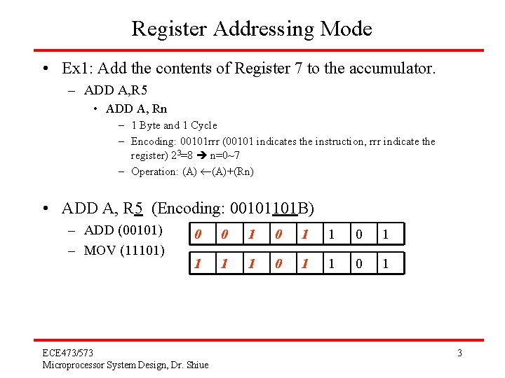
Register Addressing Mode • Ex 1: Add the contents of Register 7 to the accumulator. – ADD A, R 5 • ADD A, Rn – 1 Byte and 1 Cycle – Encoding: 00101 rrr (00101 indicates the instruction, rrr indicate the register) 23=8 n=0~7 – Operation: (A)+(Rn) • ADD A, R 5 (Encoding: 00101101 B) – ADD (00101) – MOV (11101) 0 0 1 1 0 1 1 0 1 ECE 473/573 Microprocessor System Design, Dr. Shiue 3

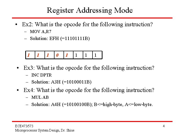
Register Addressing Mode • Ex 2: What is the opcode for the following instruction? – MOV A, R 7 – Solution: EFH (=11101111 B) 1 1 1 0 1 1 • Ex 3: What is the opcode for the following instruction? – INC DPTR – Solution: A 3 H (=10100011 B) • Ex 4: What is the opcode for the following instruction? – MUL AB – Solution: A 4 H (=10100100 B); B<=high-byte, A<=low-byte. ECE 473/573 Microprocessor System Design, Dr. Shiue 4

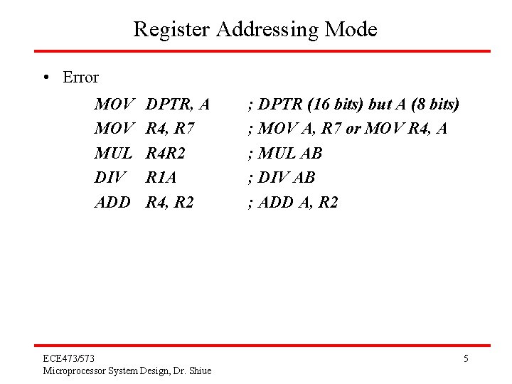
Register Addressing Mode • Error MOV MUL DIV ADD DPTR, A R 4, R 7 R 4 R 2 R 1 A R 4, R 2 ECE 473/573 Microprocessor System Design, Dr. Shiue ; DPTR (16 bits) but A (8 bits) ; MOV A, R 7 or MOV R 4, A ; MUL AB ; DIV AB ; ADD A, R 2 5

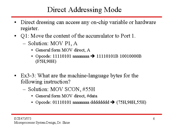
Direct Addressing Mode • Direct dressing can access any on-chip variable or hardware register. • Q 1: Move the content of the accumulator to Port 1. – Solution: MOV P 1, A • General form MOV direct, A • Opcode: 11110101 aaaa 11110101 B 10010000 B (F 5 H, 90 H) • Ex 3 -3: What are the machine-language bytes for the following instruction? – Solution: MOV SCON, #55 H • General form MOV direct, #data • Opcode: 01110101 aaaa dddd (75 H, 98 H, 55 H) ECE 473/573 Microprocessor System Design, Dr. Shiue 6

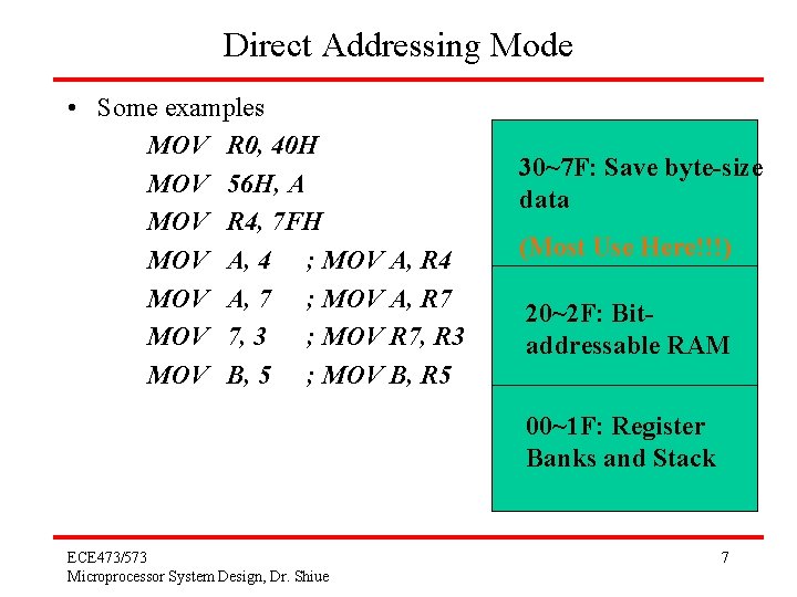
Direct Addressing Mode • Some examples MOV R 0, 40 H MOV 56 H, A MOV R 4, 7 FH MOV A, 4 ; MOV A, R 4 MOV A, 7 ; MOV A, R 7 MOV 7, 3 ; MOV R 7, R 3 MOV B, 5 ; MOV B, R 5 30~7 F: Save byte-size data (Most Use Here!!!) 20~2 F: Bitaddressable RAM 00~1 F: Register Banks and Stack ECE 473/573 Microprocessor System Design, Dr. Shiue 7

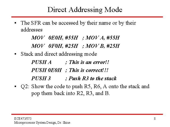
Direct Addressing Mode • The SFR can be accessed by their name or by their addresses MOV 0 E 0 H, #55 H ; MOV A, #55 H MOV 0 F 0 H, #25 H ; MOV B, #25 H • Stack and direct addressing mode PUSH A ; This is an error!! PUSH 0 E 0 H ; This is correct!!! PUSH 3 ; Push R 3 to the stack • Q 2: Show the code to push R 5, R 6, A onto the stack and pop them back into R 2, R 3, and B. ECE 473/573 Microprocessor System Design, Dr. Shiue 8

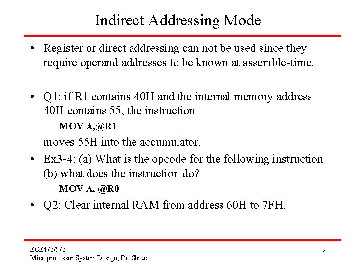
Indirect Addressing Mode • Register or direct addressing can not be used since they require operand addresses to be known at assemble-time. • Q 1: if R 1 contains 40 H and the internal memory address 40 H contains 55, the instruction MOV A, @R 1 moves 55 H into the accumulator. • Ex 3 -4: (a) What is the opcode for the following instruction (b) what does the instruction do? MOV A, @R 0 • Q 2: Clear internal RAM from address 60 H to 7 FH. ECE 473/573 Microprocessor System Design, Dr. Shiue 9

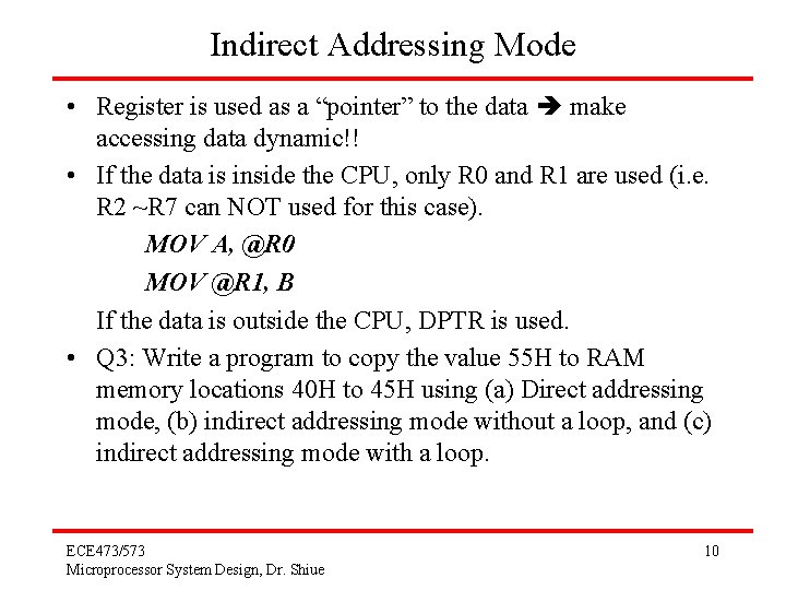
Indirect Addressing Mode • Register is used as a “pointer” to the data make accessing data dynamic!! • If the data is inside the CPU, only R 0 and R 1 are used (i. e. R 2 ~R 7 can NOT used for this case). MOV A, @R 0 MOV @R 1, B If the data is outside the CPU, DPTR is used. • Q 3: Write a program to copy the value 55 H to RAM memory locations 40 H to 45 H using (a) Direct addressing mode, (b) indirect addressing mode without a loop, and (c) indirect addressing mode with a loop. ECE 473/573 Microprocessor System Design, Dr. Shiue 10

Indirect Addressing Mode • Q 4: Write a program to clear 16 RAM locations starting at RAM address 60 H. • Q 5: Write a program to copy a block of 10 bytes of data from RAM locations starting at 35 H to RAM locations starting at 60 H. ECE 473/573 Microprocessor System Design, Dr. Shiue 11

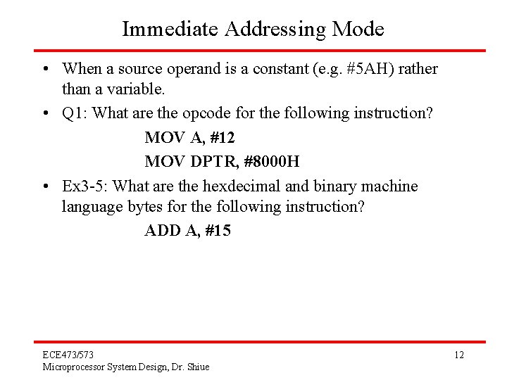
Immediate Addressing Mode • When a source operand is a constant (e. g. #5 AH) rather than a variable. • Q 1: What are the opcode for the following instruction? MOV A, #12 MOV DPTR, #8000 H • Ex 3 -5: What are the hexdecimal and binary machine language bytes for the following instruction? ADD A, #15 ECE 473/573 Microprocessor System Design, Dr. Shiue 12

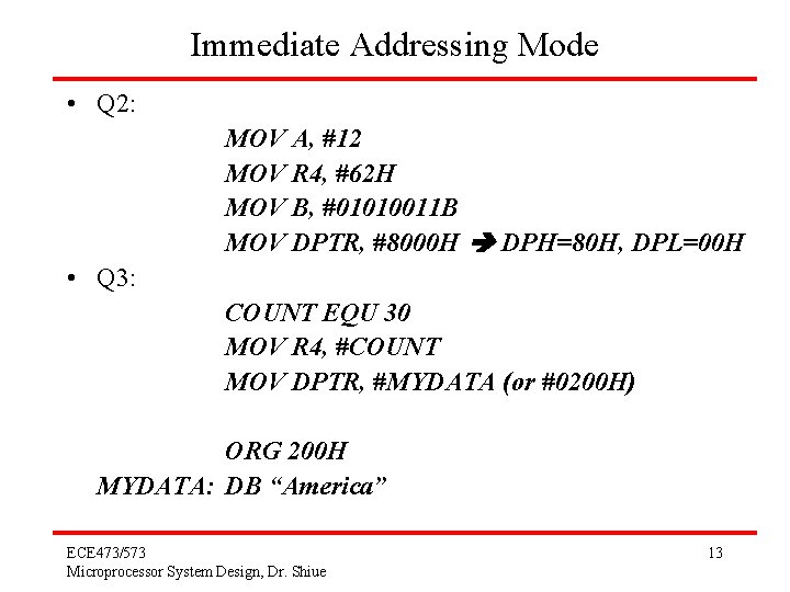
Immediate Addressing Mode • Q 2: MOV A, #12 MOV R 4, #62 H MOV B, #01010011 B MOV DPTR, #8000 H DPH=80 H, DPL=00 H • Q 3: COUNT EQU 30 MOV R 4, #COUNT MOV DPTR, #MYDATA (or #0200 H) ORG 200 H MYDATA: DB “America” ECE 473/573 Microprocessor System Design, Dr. Shiue 13

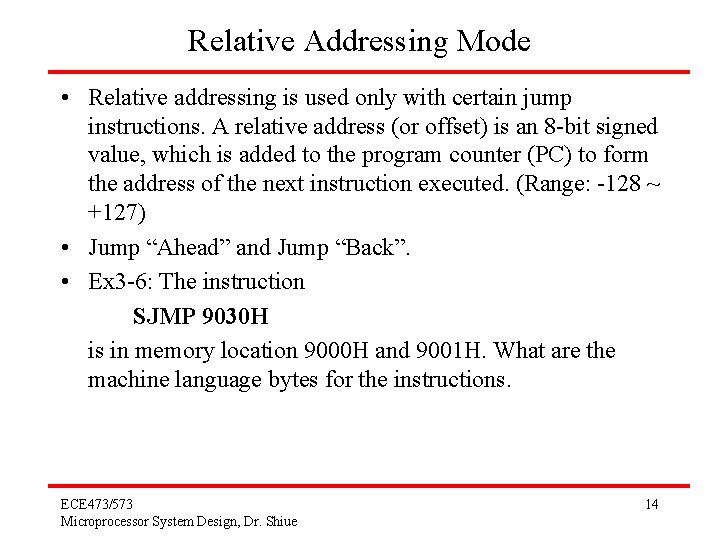
Relative Addressing Mode • Relative addressing is used only with certain jump instructions. A relative address (or offset) is an 8 -bit signed value, which is added to the program counter (PC) to form the address of the next instruction executed. (Range: -128 ~ +127) • Jump “Ahead” and Jump “Back”. • Ex 3 -6: The instruction SJMP 9030 H is in memory location 9000 H and 9001 H. What are the machine language bytes for the instructions. ECE 473/573 Microprocessor System Design, Dr. Shiue 14

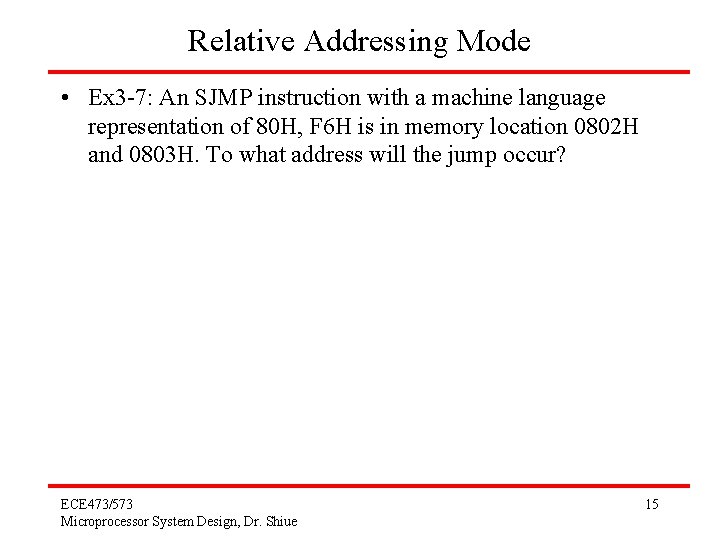
Relative Addressing Mode • Ex 3 -7: An SJMP instruction with a machine language representation of 80 H, F 6 H is in memory location 0802 H and 0803 H. To what address will the jump occur? ECE 473/573 Microprocessor System Design, Dr. Shiue 15

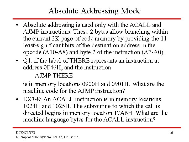
Absolute Addressing Mode • Absolute addressing is used only with the ACALL and AJMP instructions. These 2 bytes allow branching within the current 2 K page of code memory by providing the 11 least-significant bits of the destination address in the opcode (A 10 -A 8) and byte 2 of the instruction (A 7 -A 0). • Q 1: if the label of THERE represents an instruction at address 0 F 46 H, and the instruction AJMP THERE is in memory locations 0900 H and 0901 H. What are the machine code for the AJMP instruction? • EX 3 -8: An ACALL instruction is in memory locations 1024 H and 1025 H. The subroutine to which the call is directed begins in memory location 17 A 6 H. What are the machine language bytes for the ACALL instruction? ECE 473/573 Microprocessor System Design, Dr. Shiue 16

Long Addressing Mode • Long addressing is used only with the LCALL and LJMP instructions. These 3 -byte instructions include a full 16 -bit destination address. The advantage is that the full 64 K code space may be used. • Ex 3 -9: What are the machine language bytes for the following instruction? LJMP 8 AF 2 H ECE 473/573 Microprocessor System Design, Dr. Shiue 17

Index Addressing Mode • Indexed addressing mode and on-chip ROM access is used in accessing data elements of look-up table entries located in the program ROM. • Indexed addressing uses a base register (PC or DPTR) and an offset (ACC) in forming the effective address for a JMP or MOVC instruction. Jump tables or look-up tables are easily created using indexed addressing. • MOVC: this is because the data element is stored in ROM rather than RAM. Here ‘C’ denotes Code (ROM). • Ex 3 -10: What is the opcode for the following instruction? MOVC A, @A+DPTR ECE 473/573 Microprocessor System Design, Dr. Shiue 18

Index Addressing Mode • Q 1: In this program, assume that the word ‘USA’ is burned into ROM locations starting at 200 H, and that the program is burned into ROM location starting at 0 H. • Q 2: Assuming that ROM space starting at 250 H contains “America”, write a program to transfer the bytes into RAM locations starting at 40 H. ECE 473/573 Microprocessor System Design, Dr. Shiue 19

Look-up Tables and the Use of Index Addressing Mode • Q 3: Write a program to get the x value from P 1 and send x 2 to P 2 continuously. ECE 473/573 Microprocessor System Design, Dr. Shiue 20

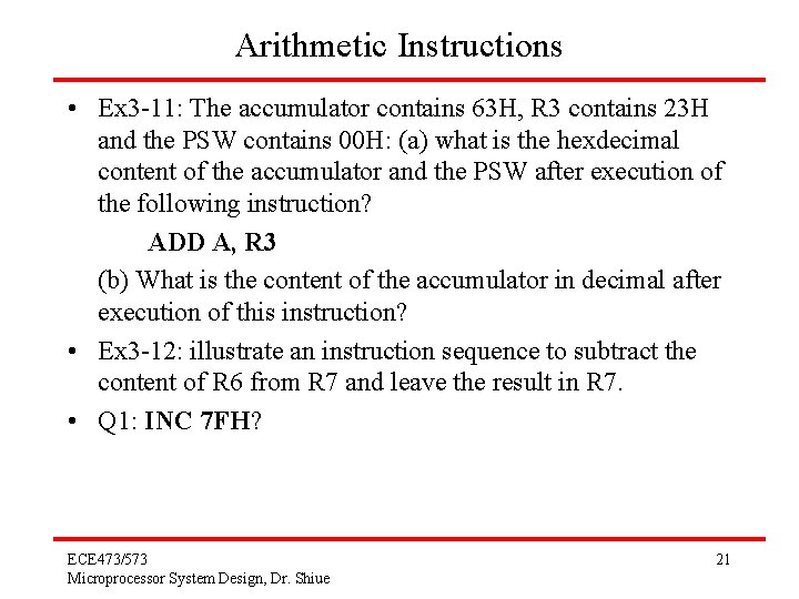
Arithmetic Instructions • Ex 3 -11: The accumulator contains 63 H, R 3 contains 23 H and the PSW contains 00 H: (a) what is the hexdecimal content of the accumulator and the PSW after execution of the following instruction? ADD A, R 3 (b) What is the content of the accumulator in decimal after execution of this instruction? • Ex 3 -12: illustrate an instruction sequence to subtract the content of R 6 from R 7 and leave the result in R 7. • Q 1: INC 7 FH? ECE 473/573 Microprocessor System Design, Dr. Shiue 21

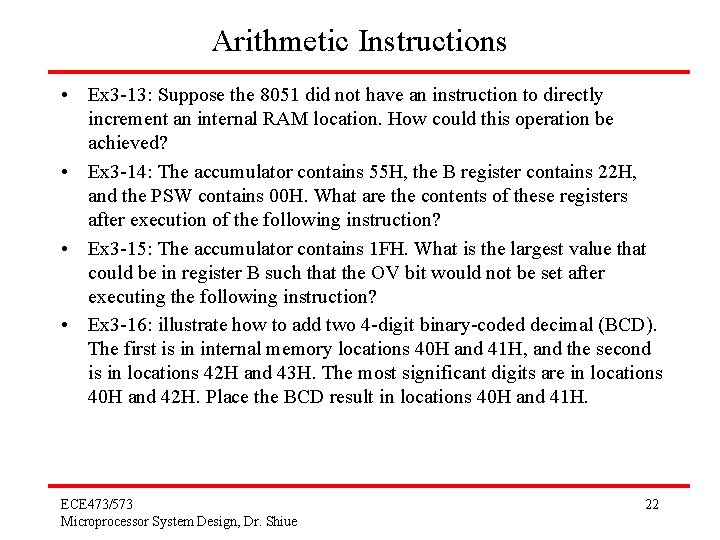
Arithmetic Instructions • Ex 3 -13: Suppose the 8051 did not have an instruction to directly increment an internal RAM location. How could this operation be achieved? • Ex 3 -14: The accumulator contains 55 H, the B register contains 22 H, and the PSW contains 00 H. What are the contents of these registers after execution of the following instruction? • Ex 3 -15: The accumulator contains 1 FH. What is the largest value that could be in register B such that the OV bit would not be set after executing the following instruction? • Ex 3 -16: illustrate how to add two 4 -digit binary-coded decimal (BCD). The first is in internal memory locations 40 H and 41 H, and the second is in locations 42 H and 43 H. The most significant digits are in locations 40 H and 42 H. Place the BCD result in locations 40 H and 41 H. ECE 473/573 Microprocessor System Design, Dr. Shiue 22

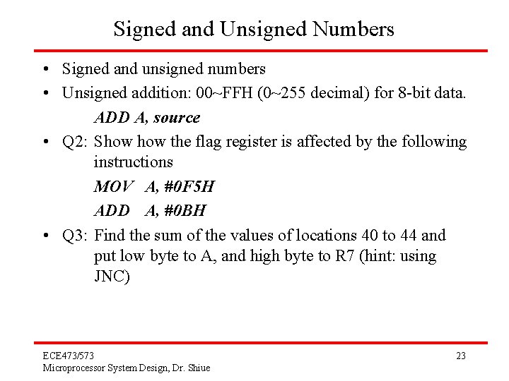
Signed and Unsigned Numbers • Signed and unsigned numbers • Unsigned addition: 00~FFH (0~255 decimal) for 8 -bit data. ADD A, source • Q 2: Show the flag register is affected by the following instructions MOV A, #0 F 5 H ADD A, #0 BH • Q 3: Find the sum of the values of locations 40 to 44 and put low byte to A, and high byte to R 7 (hint: using JNC) ECE 473/573 Microprocessor System Design, Dr. Shiue 23

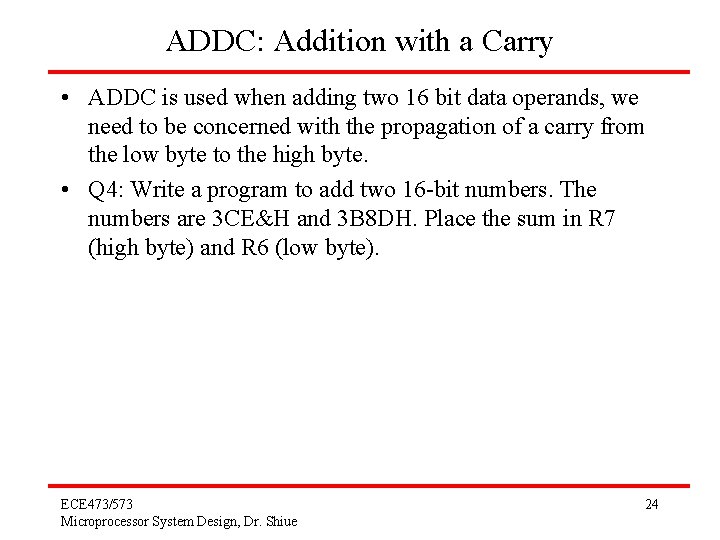
ADDC: Addition with a Carry • ADDC is used when adding two 16 bit data operands, we need to be concerned with the propagation of a carry from the low byte to the high byte. • Q 4: Write a program to add two 16 -bit numbers. The numbers are 3 CE&H and 3 B 8 DH. Place the sum in R 7 (high byte) and R 6 (low byte). ECE 473/573 Microprocessor System Design, Dr. Shiue 24

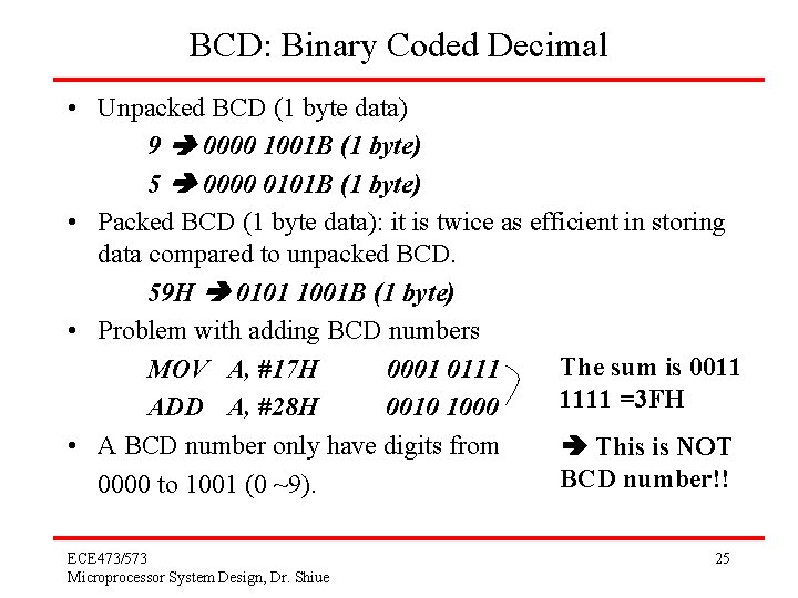
BCD: Binary Coded Decimal • Unpacked BCD (1 byte data) 9 0000 1001 B (1 byte) 5 0000 0101 B (1 byte) • Packed BCD (1 byte data): it is twice as efficient in storing data compared to unpacked BCD. 59 H 0101 1001 B (1 byte) • Problem with adding BCD numbers The sum is 0011 MOV A, #17 H 0001 0111 1111 =3 FH ADD A, #28 H 0010 1000 • A BCD number only have digits from This is NOT BCD number!! 0000 to 1001 (0 ~9). ECE 473/573 Microprocessor System Design, Dr. Shiue 25

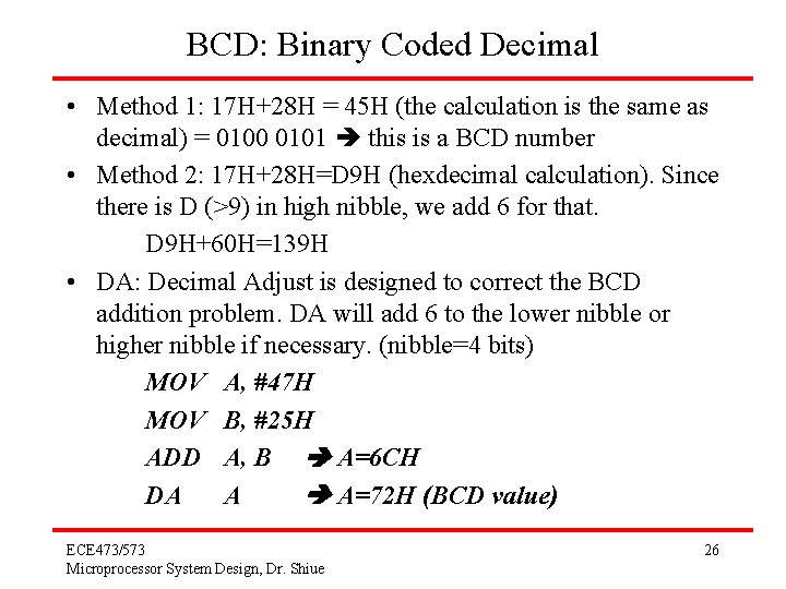
BCD: Binary Coded Decimal • Method 1: 17 H+28 H = 45 H (the calculation is the same as decimal) = 0100 0101 this is a BCD number • Method 2: 17 H+28 H=D 9 H (hexdecimal calculation). Since there is D (>9) in high nibble, we add 6 for that. D 9 H+60 H=139 H • DA: Decimal Adjust is designed to correct the BCD addition problem. DA will add 6 to the lower nibble or higher nibble if necessary. (nibble=4 bits) MOV A, #47 H MOV B, #25 H ADD A, B A=6 CH DA A A=72 H (BCD value) ECE 473/573 Microprocessor System Design, Dr. Shiue 26

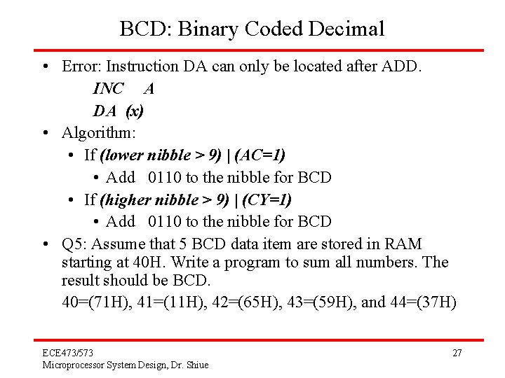
BCD: Binary Coded Decimal • Error: Instruction DA can only be located after ADD. INC A DA (x) • Algorithm: • If (lower nibble > 9) | (AC=1) • Add 0110 to the nibble for BCD • If (higher nibble > 9) | (CY=1) • Add 0110 to the nibble for BCD • Q 5: Assume that 5 BCD data item are stored in RAM starting at 40 H. Write a program to sum all numbers. The result should be BCD. 40=(71 H), 41=(11 H), 42=(65 H), 43=(59 H), and 44=(37 H) ECE 473/573 Microprocessor System Design, Dr. Shiue 27

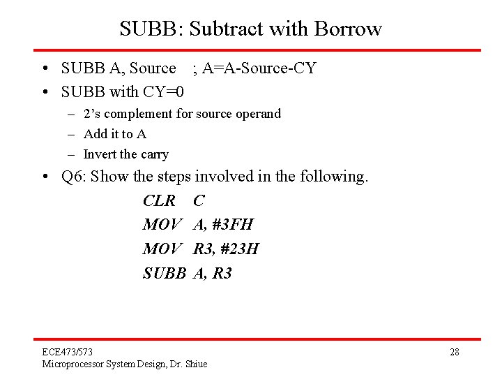
SUBB: Subtract with Borrow • SUBB A, Source ; A=A-Source-CY • SUBB with CY=0 – 2’s complement for source operand – Add it to A – Invert the carry • Q 6: Show the steps involved in the following. CLR C MOV A, #3 FH MOV R 3, #23 H SUBB A, R 3 ECE 473/573 Microprocessor System Design, Dr. Shiue 28

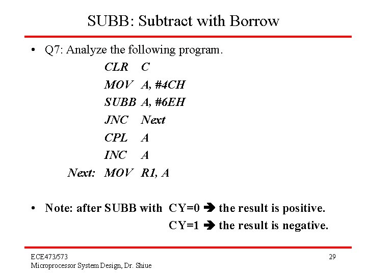
SUBB: Subtract with Borrow • Q 7: Analyze the following program. CLR C MOV A, #4 CH SUBB A, #6 EH JNC Next CPL A INC A Next: MOV R 1, A • Note: after SUBB with CY=0 the result is positive. CY=1 the result is negative. ECE 473/573 Microprocessor System Design, Dr. Shiue 29

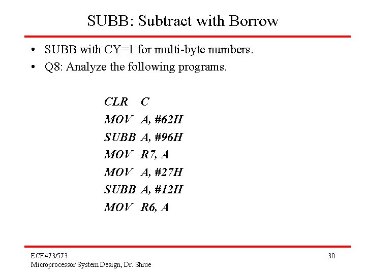
SUBB: Subtract with Borrow • SUBB with CY=1 for multi-byte numbers. • Q 8: Analyze the following programs. CLR MOV SUBB MOV C A, #62 H A, #96 H R 7, A A, #27 H A, #12 H R 6, A ECE 473/573 Microprocessor System Design, Dr. Shiue 30

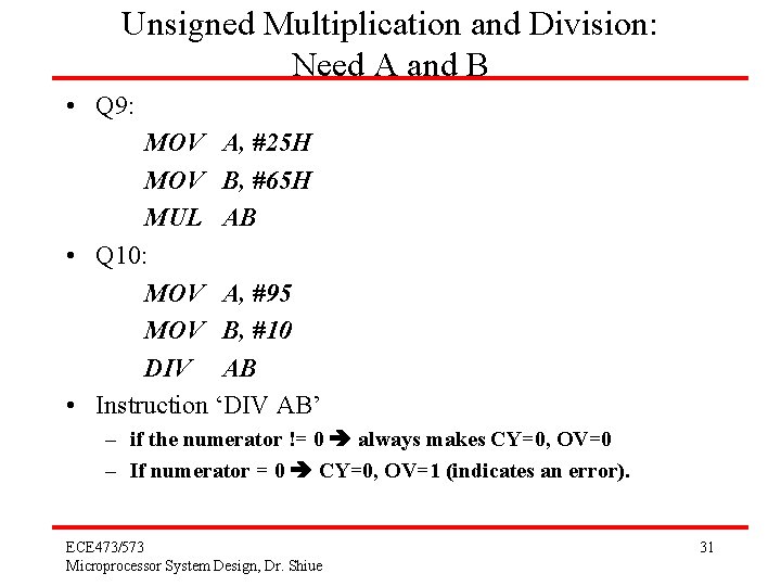
Unsigned Multiplication and Division: Need A and B • Q 9: MOV A, #25 H MOV B, #65 H MUL AB • Q 10: MOV A, #95 MOV B, #10 DIV AB • Instruction ‘DIV AB’ – if the numerator != 0 always makes CY=0, OV=0 – If numerator = 0 CY=0, OV=1 (indicates an error). ECE 473/573 Microprocessor System Design, Dr. Shiue 31

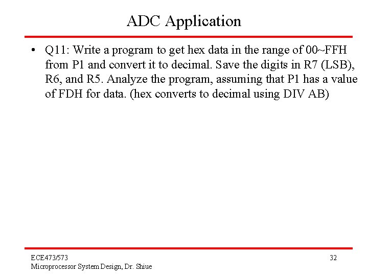
ADC Application • Q 11: Write a program to get hex data in the range of 00~FFH from P 1 and convert it to decimal. Save the digits in R 7 (LSB), R 6, and R 5. Analyze the program, assuming that P 1 has a value of FDH for data. (hex converts to decimal using DIV AB) ECE 473/573 Microprocessor System Design, Dr. Shiue 32

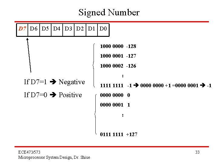
Signed Number D 7 D 6 D 5 D 4 D 3 D 2 D 1 D 0 1000 0000 -128 1000 0001 -127 1000 0002 -126 : If D 7=1 Negative 1111 -1 0000 +1 =0000 0001 -1 If D 7=0 Positive 0000 0 0001 1 : 0111 1111 +127 ECE 473/573 Microprocessor System Design, Dr. Shiue 33

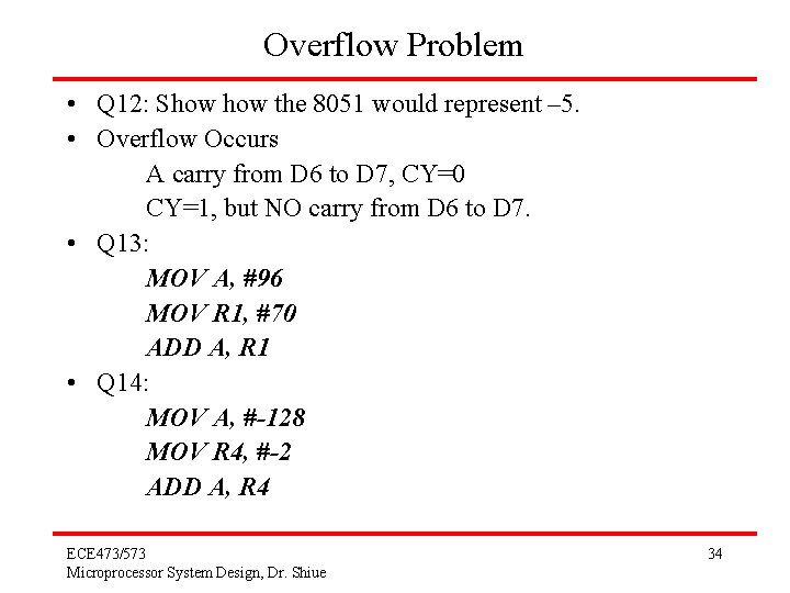
Overflow Problem • Q 12: Show the 8051 would represent – 5. • Overflow Occurs A carry from D 6 to D 7, CY=0 CY=1, but NO carry from D 6 to D 7. • Q 13: MOV A, #96 MOV R 1, #70 ADD A, R 1 • Q 14: MOV A, #-128 MOV R 4, #-2 ADD A, R 4 ECE 473/573 Microprocessor System Design, Dr. Shiue 34

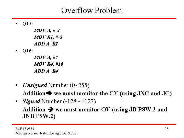
Overflow Problem • Q 15: MOV A, #-2 MOV R 1, #-5 ADD A, R 1 • Q 16: MOV A, #7 MOV R 4, #18 ADD A, R 4 • Unsigned Number (0~255) Addition we must monitor the CY (using JNC and JC) • Signed Number (-128 ~+127) Addition we must monitor OV (using JB PSW. 2 and JNB PSW. 2) ECE 473/573 Microprocessor System Design, Dr. Shiue 35

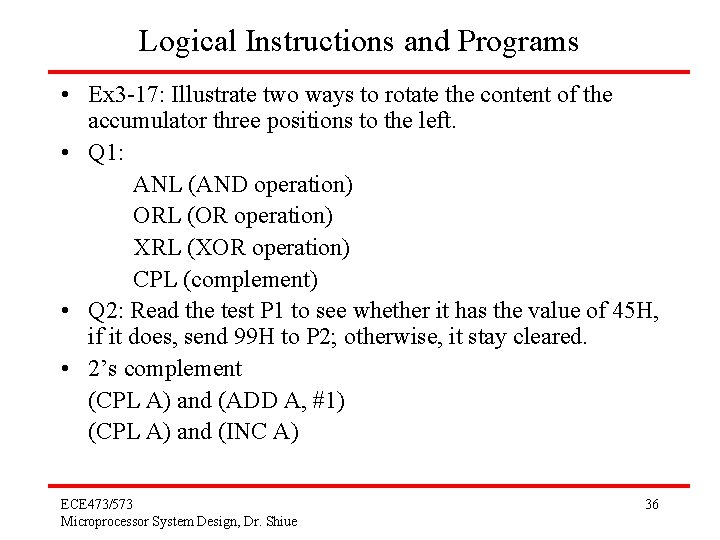
Logical Instructions and Programs • Ex 3 -17: Illustrate two ways to rotate the content of the accumulator three positions to the left. • Q 1: ANL (AND operation) ORL (OR operation) XRL (XOR operation) CPL (complement) • Q 2: Read the test P 1 to see whether it has the value of 45 H, if it does, send 99 H to P 2; otherwise, it stay cleared. • 2’s complement (CPL A) and (ADD A, #1) (CPL A) and (INC A) ECE 473/573 Microprocessor System Design, Dr. Shiue 36

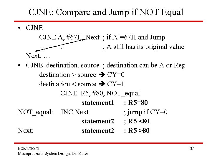
CJNE: Compare and Jump if NOT Equal • CJNE A, #67 H, Next ; if A!=67 H and Jump : ; A still has its original value Next: … • CJNE destination, source ; destination can be A or Reg destination > source CY=0 destination < source CY=1 CJNE R 5, #80, NOT_equal statement 1 ; R 5=80 NOT_equal: JNC Next ; jump if CY=0 statement 2 ; R 5 <80 Next: statement 2 ; R 5 >80 ECE 473/573 Microprocessor System Design, Dr. Shiue 37

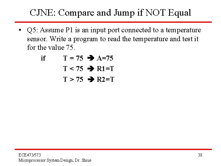
CJNE: Compare and Jump if NOT Equal • Q 5: Assume P 1 is an input port connected to a temperature sensor. Write a program to read the temperature and test it for the value 75. if T = 75 A=75 T < 75 R 1=T T > 75 R 2=T ECE 473/573 Microprocessor System Design, Dr. Shiue 38

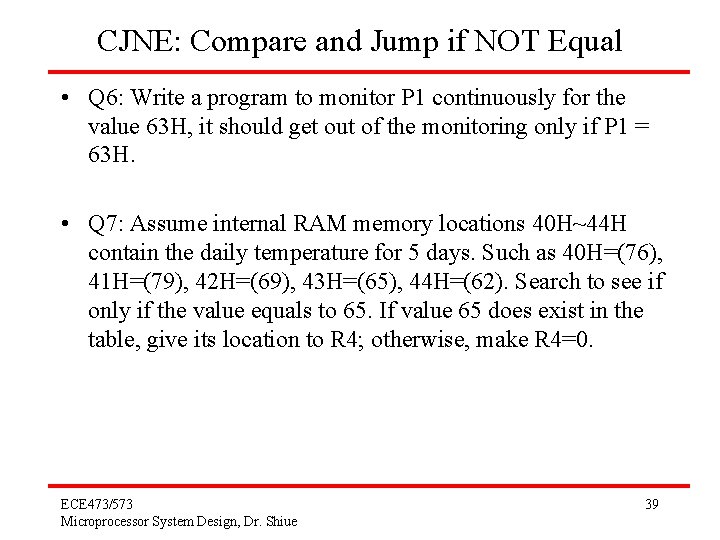
CJNE: Compare and Jump if NOT Equal • Q 6: Write a program to monitor P 1 continuously for the value 63 H, it should get out of the monitoring only if P 1 = 63 H. • Q 7: Assume internal RAM memory locations 40 H~44 H contain the daily temperature for 5 days. Such as 40 H=(76), 41 H=(79), 42 H=(69), 43 H=(65), 44 H=(62). Search to see if only if the value equals to 65. If value 65 does exist in the table, give its location to R 4; otherwise, make R 4=0. ECE 473/573 Microprocessor System Design, Dr. Shiue 39

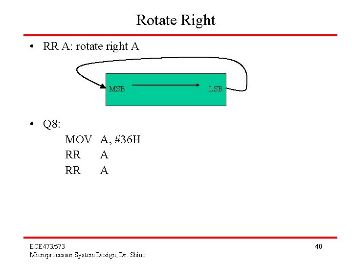
Rotate Right • RR A: rotate right A MSB LSB • Q 8: MOV A, #36 H RR A ECE 473/573 Microprocessor System Design, Dr. Shiue 40

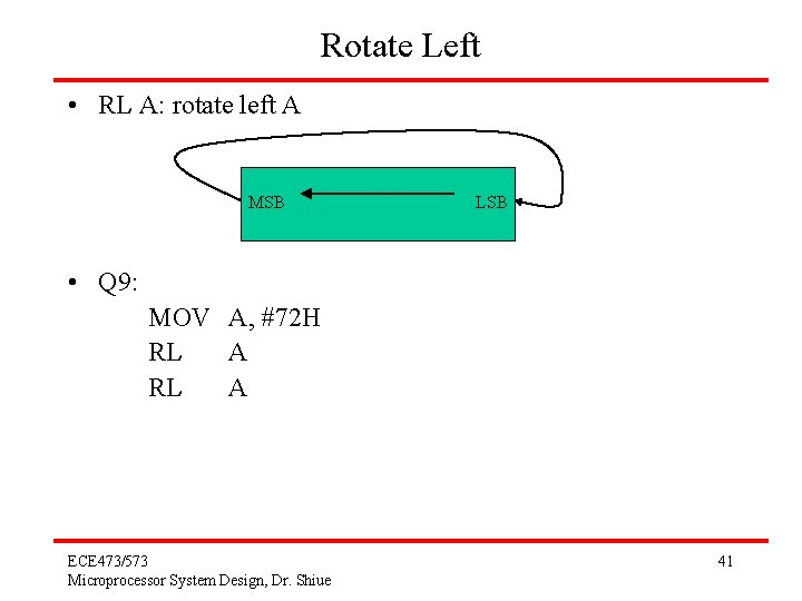
Rotate Left • RL A: rotate left A MSB LSB • Q 9: MOV A, #72 H RL A ECE 473/573 Microprocessor System Design, Dr. Shiue 41

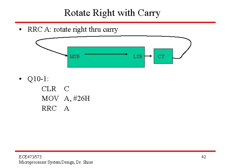
Rotate Right with Carry • RRC A: rotate right thru carry MSB LSB CY • Q 10 -1: CLR C MOV A, #26 H RRC A ECE 473/573 Microprocessor System Design, Dr. Shiue 42

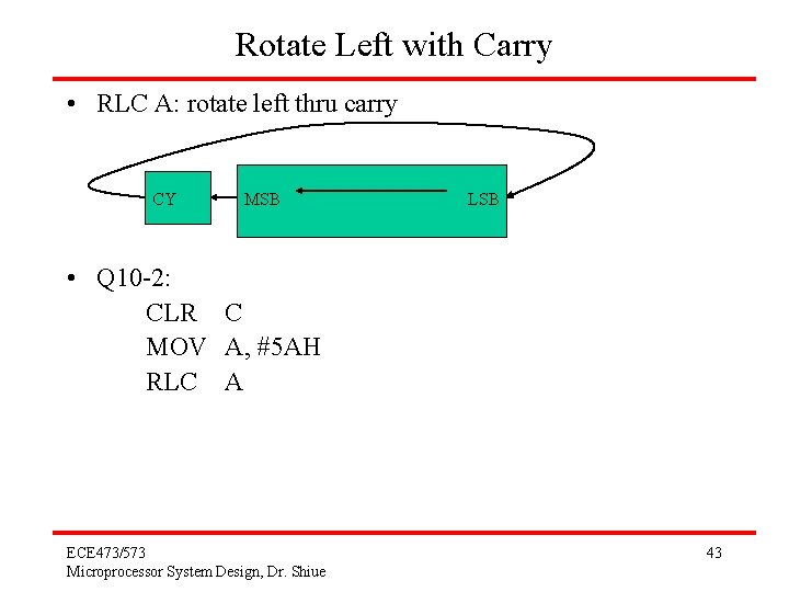
Rotate Left with Carry • RLC A: rotate left thru carry CY MSB LSB • Q 10 -2: CLR C MOV A, #5 AH RLC A ECE 473/573 Microprocessor System Design, Dr. Shiue 43

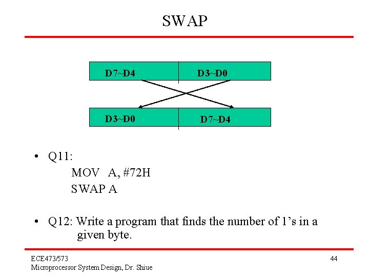
SWAP D 7~D 4 D 3~D 0 D 7~D 4 • Q 11: MOV A, #72 H SWAP A • Q 12: Write a program that finds the number of 1’s in a given byte. ECE 473/573 Microprocessor System Design, Dr. Shiue 44

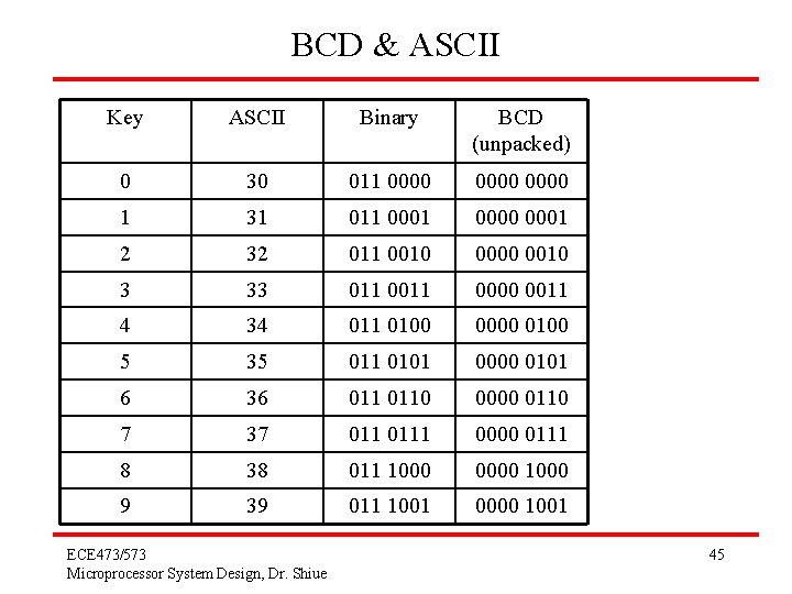
BCD & ASCII Key ASCII Binary BCD (unpacked) 0 30 011 0000 1 31 011 0000 0001 2 32 011 0010 0000 0010 3 33 011 0000 0011 4 34 011 0100 0000 0100 5 35 011 0101 0000 0101 6 36 0110 0000 0110 7 37 0111 0000 0111 8 38 011 1000 0000 1000 9 39 011 1001 0000 1001 ECE 473/573 Microprocessor System Design, Dr. Shiue 45

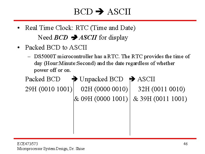
BCD ASCII • Real Time Clock: RTC (Time and Date) Need BCD ASCII for display • Packed BCD to ASCII – DS 5000 T microcontroller has a RTC. The RTC provides the time of day (Hour: Minute: Second) and the date regardless of whether power off or on. Packed BCD Unpacked BCD ASCII 29 H (0010 1001) 02 H (0000 0010) 32 H (0011 0010) & 09 H (0000 1001) & 39 H (0011 1001) ECE 473/573 Microprocessor System Design, Dr. Shiue 46

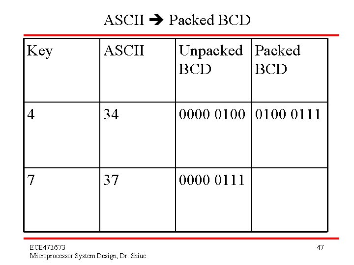
ASCII Packed BCD Key ASCII Unpacked Packed BCD 4 34 0000 0100 0111 7 37 0000 0111 ECE 473/573 Microprocessor System Design, Dr. Shiue 47

Example: Packed BCD ASCII • Q 13: Assume the register A has packed BCD, write a program to convert packed BCD to two ASCII numbers and place them in R 2 and R 6. ECE 473/573 Microprocessor System Design, Dr. Shiue 48

Data Transfer Instructions • Ex 3 -22: illustrate an instruction sequence to read the content of external RAM locations 10 F 4 H and 10 F 5 H and place the values read in R 6 and R 7, respectively. • Ex 3 -23: Write a subroutine called SQUARE to compute the square of an integer between 0 and 9. Enter the subroutine with the integer in A, and return with the square of the integer in A. Write two versions of the subroutine: (a) using a look-up table, and (b) without using a look-up table. Then (c) illustrate a call sequence to convert 6 to its square, 36. ECE 473/573 Microprocessor System Design, Dr. Shiue 49

Boolean Instructions • Q 1: Write an instruction sequence for the AND gate. ECE 473/573 Microprocessor System Design, Dr. Shiue 50