Instruction Formats 1 Book Chapter Computer Organization and
Instruction Formats 1
Book Chapter § § “Computer Organization and Architecture” Author “William Stallings” 8 th Edition Chapter 11 § Section 11. 3 2
Instruction Format (1/2) § Defines the layout of the bits in an instruction § Operation Code (opcode) § Necessary instruction element § Tells the CPU what to do § Source/destination Operands § An instruction can have zero or more operands § Operands are referenced using one the addressing modes § Basic design issues in Instruction Format are § Instruction Length § Allocation of bits 3
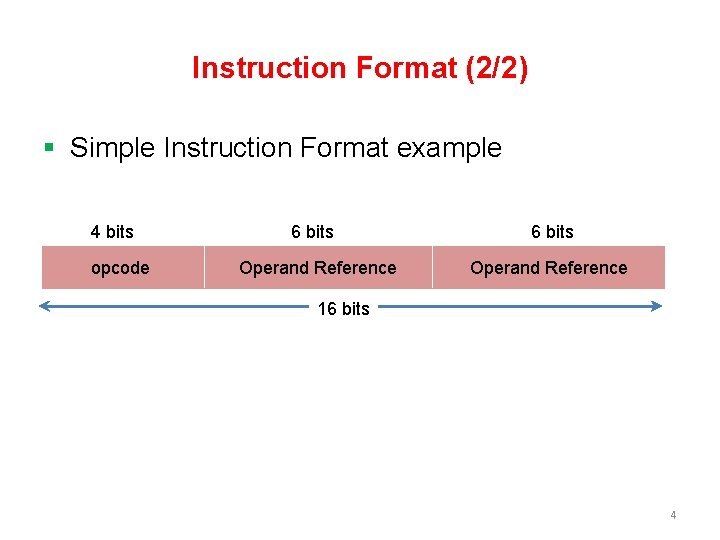
Instruction Format (2/2) § Simple Instruction Format example 4 bits opcode 6 bits Operand Reference 16 bits 4
Instruction Length § Instruction Length affects and is affected by § § § Memory size Memory organization Bus structure Processor complexity Processor speed § Trade off between powerful instruction repertoire and saving space 5
Allocation of Bits § More operations in an instruction set requires more opcodes § More opcodes means more bits in opcode field and less bits in operand references § Following factors help to determine the use of addressing bits § § § Number of addressing modes Number of operands Register versus Memory Number of register sets Address range Address granularity 6
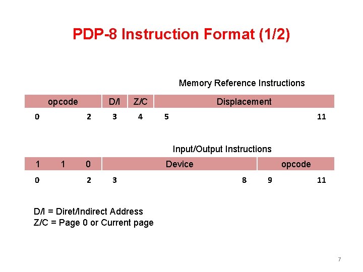
PDP-8 Instruction Format (1/2) Memory Reference Instructions opcode 0 2 D/I Z/C 3 4 Displacement 5 11 Input/Output Instructions 1 0 2 Device 3 opcode 8 9 11 D/I = Diret/Indirect Address Z/C = Page 0 or Current page 7

PDP-8 Instruction Format (2/2) Register Reference Instructions 1 1 1 0 CLA CLL CMA CML RAR RAL BSW IAC 0 1 2 3 4 5 6 7 8 9 10 11 1 0 CLA SMA SZA SNL RSS OSR HLT 0 0 1 2 3 4 5 6 7 8 9 10 11 1 0 CLA MQA 0 MQL 0 0 0 1 2 3 4 5 6 7 8 9 10 11 CLA = Clear Accumulator CLL = Clear Link CMA= Co. Mplement Accumulator CML= Co. Mplement Link RAR= Rotate Accumulator Right RAL= Rotate Accumulator Left BSW= Byte SWap IAC = Increment ACcumulator SMA= Skip on Minus Accumulator SZA= Skip on Zero Accumulator SNL= Skip on Nonzero Link RSS= Reverse Skip Sense OSR= Or with Switch Register HLT= Ha. LT MQA=Multiplier Quotient into Accumulator MQL=Multiplier Quotient Load 8
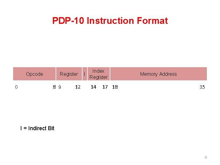
PDP-10 Instruction Format Opcode 0 Register 8 9 12 I Index Register 14 17 18 Memory Address 35 I = Indirect Bit 9
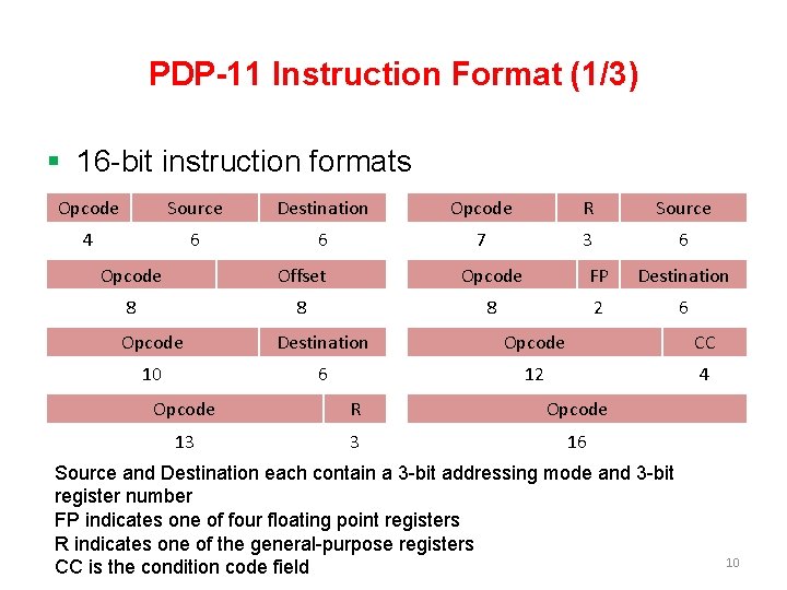
PDP-11 Instruction Format (1/3) § 16 -bit instruction formats Opcode Source Destination Opcode R Source 4 6 6 7 3 6 Opcode Offset Opcode FP Destination 8 8 8 2 6 Opcode Destination Opcode CC 10 6 12 4 Opcode R Opcode 13 3 16 Source and Destination each contain a 3 -bit addressing mode and 3 -bit register number FP indicates one of four floating point registers R indicates one of the general-purpose registers CC is the condition code field 10
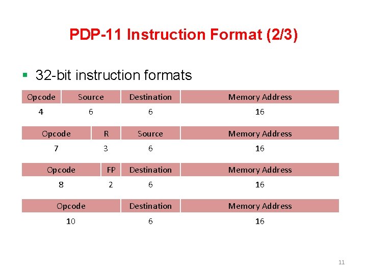
PDP-11 Instruction Format (2/3) § 32 -bit instruction formats Opcode Source Destination Memory Address 4 6 6 16 Opcode R Source Memory Address 7 3 6 16 Opcode FP Destination Memory Address 8 2 6 16 Opcode Destination Memory Address 10 6 16 11
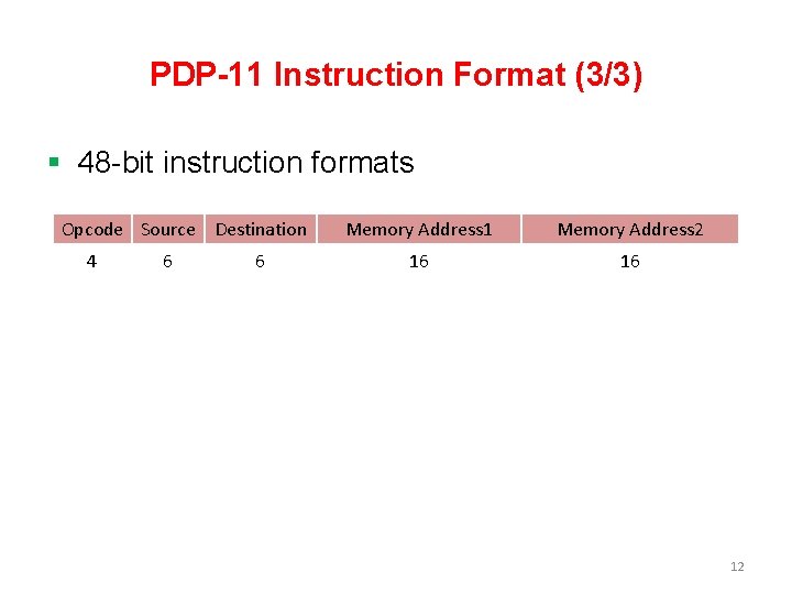
PDP-11 Instruction Format (3/3) § 48 -bit instruction formats Opcode Source Destination 4 6 6 Memory Address 1 Memory Address 2 16 16 12
- Slides: 12