inst eecs berkeley educs 61 c CS 61
inst. eecs. berkeley. edu/~cs 61 c CS 61 C : Machine Structures Lecture 20 CPU Design: Control II & Pipelining I 2010 -07 -26 TA Noah Johnson CS 61 C L 20 CPU Design: Control II and Pipelining I (1) http: //xkcd. com/676/ Johnson, Summer 2010 © UCB
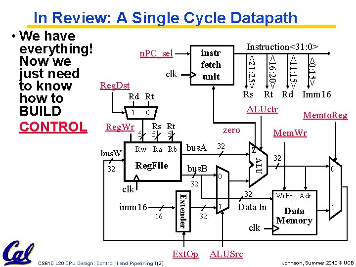
In Review: A Single Cycle Datapath Instruction<31: 0> Rs Rt Rd Imm 16 ALUctr Memto. Reg Rd Rt 1 Reg. Wr 0 5 Rs Rt 5 bus. B 32 16 Extender clk imm 16 bus. A Ext. Op CS 61 C L 20 CPU Design: Control II and Pipelining I (2) 32 Mem. Wr Z ALU Reg. File 32 zero 5 Rw Ra Rb bus. W <0: 15> Reg. Dst <11: 15> clk <16: 20> instr fetch unit n. PC_sel <21: 25> • We have everything! Now we just need to know how to BUILD CONTROL 0 32 1 32 Data In clk 32 0 Wr. En Adr Data Memory 1 ALUSrc Johnson, Summer 2010 © UCB
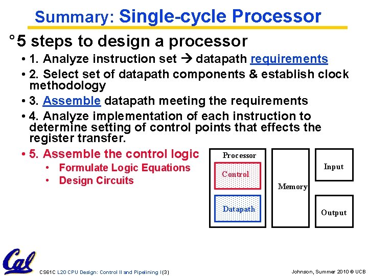
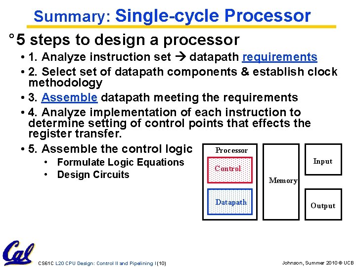
Summary: Single-cycle Processor ° 5 steps to design a processor • 1. Analyze instruction set datapath requirements • 2. Select set of datapath components & establish clock methodology • 3. Assemble datapath meeting the requirements • 4. Analyze implementation of each instruction to determine setting of control points that effects the register transfer. • 5. Assemble the control logic Processor • Formulate Logic Equations • Design Circuits Control Memory Datapath CS 61 C L 20 CPU Design: Control II and Pipelining I (3) Input Output Johnson, Summer 2010 © UCB
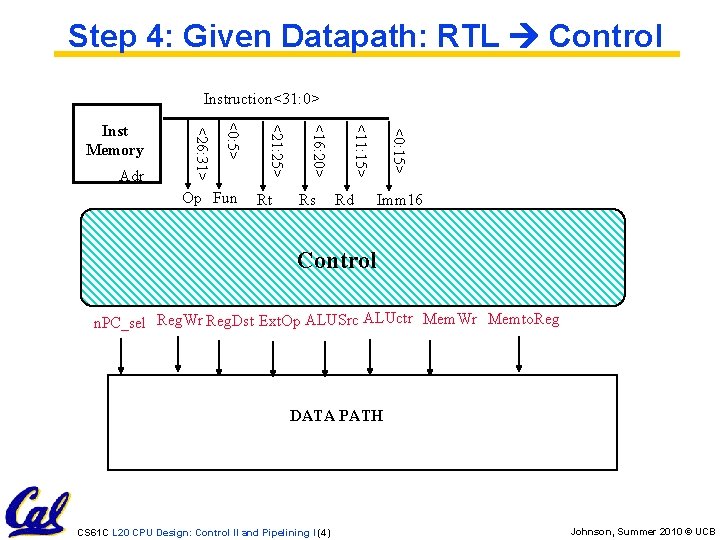
Step 4: Given Datapath: RTL Control Instruction<31: 0> Rd <0: 15> Rs <11: 15> Rt <16: 20> Op Fun <21: 25> <0: 5> Adr <26: 31> Inst Memory Imm 16 Control n. PC_sel Reg. Wr Reg. Dst Ext. Op ALUSrc ALUctr Mem. Wr Memto. Reg DATA PATH CS 61 C L 20 CPU Design: Control II and Pipelining I (4) Johnson, Summer 2010 © UCB
![A Summary of the Control Signals (1/2) inst Register Transfer add R[rd] R[rs] + A Summary of the Control Signals (1/2) inst Register Transfer add R[rd] R[rs] +](http://slidetodoc.com/presentation_image_h2/1b3a9e43c178b04252987d4421876e7e/image-5.jpg)
A Summary of the Control Signals (1/2) inst Register Transfer add R[rd] R[rs] + R[rt]; PC + 4 ALUsrc = Reg. B, ALUctr = “ADD”, Reg. Dst = rd, Reg. Wr, n. PC_sel = “+4” sub R[rd] R[rs] – R[rt]; PC + 4 ALUsrc = Reg. B, ALUctr = “SUB”, Reg. Dst = rd, Reg. Wr, n. PC_sel = “+4” ori R[rt] R[rs] + zero_ext(Imm 16); PC + 4 ALUsrc = Im, Extop = “Z”, ALUctr = “OR”, Reg. Dst = rt, Reg. Wr, n. PC_sel =“+4” lw R[rt] MEM[ R[rs] + sign_ext(Imm 16)]; PC + 4 ALUsrc = Im, Extop = “sn”, ALUctr = “ADD”, Reg. Dst = rt, Reg. Wr, n. PC_sel = “+4” sw Memto. Reg, MEM[ R[rs] + sign_ext(Imm 16)] R[rs]; PC + 4 ALUsrc = Im, Extop = “sn”, ALUctr = “ADD”, Mem. Wr, n. PC_sel = “+4” beq if ( R[rs] == R[rt] ) then PC + sign_ext(Imm 16)] || 00 else PC + 4 n. PC_sel = “br”, ALUctr = “SUB” CS 61 C L 20 CPU Design: Control II and Pipelining I (5) Johnson, Summer 2010 © UCB
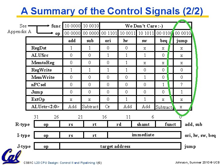
A Summary of the Control Signals (2/2) See Appendix A func 10 0000 10 0010 We Don’t Care : -) op 00 0000 00 1101 10 0011 10 1011 00 0100 00 0010 ALUSrc Memto. Reg. Write Mem. Write add 1 0 0 1 0 sub 1 0 0 1 0 ori 0 1 0 lw 0 1 1 1 0 sw x 1 x 0 1 n. PCsel Jump Ext. Op ALUctr<2: 0> 0 0 x Add 0 0 x Subtract 0 0 0 Or 0 0 1 Add Reg. Dst 31 26 21 16 R-type op rs rt I-type op rs rt J-type op 11 rd CS 61 C L 20 CPU Design: Control II and Pipelining I (6) jump x x x 0 0 1 0 x ? 1 x x Subtract 6 shamt immediate target address beq x 0 0 0 funct add, sub ori, lw, sw, beq jump Johnson, Summer 2010 © UCB
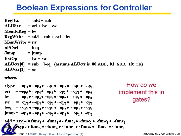
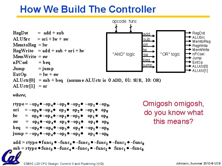
Boolean Expressions for Controller Reg. Dst ALUSrc Memto. Reg. Write Mem. Write n. PCsel Jump Ext. Op ALUctr[0] ALUctr[1] = add + sub = ori + lw + sw = lw = add + sub + ori + lw = sw = beq = jump = lw + sw = sub + beq (assume ALUctr is 00 ADD, 01: SUB, 10: OR) = or where, rtype = ~op 5 ~op 4 ~op 3 ~op 2 ori = ~op 5 ~op 4 op 3 op 2 lw = op 5 ~op 4 ~op 3 ~op 2 sw = op 5 ~op 4 op 3 ~op 2 beq = ~op 5 ~op 4 ~op 3 op 2 jump = ~op 5 ~op 4 ~op 3 ~op 2 ~op 1 ~op 0, ~op 1 op 0 ~op 1 ~op 0 How do we implement this in gates? add = rtype func 5 ~func 4 ~func 3 ~func 2 ~func 1 ~func 0 sub = rtype func 5 ~func 4 ~func 3 ~func 2 func 1 ~func 0 CS 61 C L 20 CPU Design: Control II and Pipelining I (7) Johnson, Summer 2010 © UCB
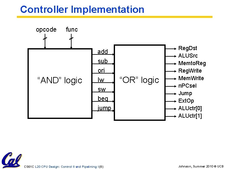
Controller Implementation opcode func “AND” logic add sub ori lw sw beq jump CS 61 C L 20 CPU Design: Control II and Pipelining I (8) “OR” logic Reg. Dst ALUSrc Memto. Reg. Write Mem. Write n. PCsel Jump Ext. Op ALUctr[0] ALUctr[1] Johnson, Summer 2010 © UCB
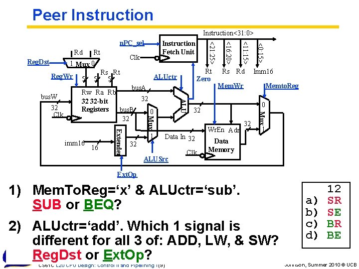
Peer Instruction<31: 0> Reg. Wr Rs Rt 5 Extender 16 1 32 Clk Imm 16 Mem. Wr Memto. Reg 0 32 Data In 32 ALUSrc Rs Rd Wr. En Adr 32 Mux bus. A Rw Ra Rb 32 32 32 -bit Registers bus. B 0 32 imm 16 Rt Zero ALUctr Mux 32 Clk 5 ALU bus. W 5 <0: 15> Clk 1 Mux 0 <11: 15> Reg. Dst Rt <21: 25> Rd Instruction Fetch Unit <16: 20> n. PC_sel 1 Data Memory Ext. Op 1) Mem. To. Reg=‘x’ & ALUctr=‘sub’. SUB or BEQ? 2) ALUctr=‘add’. Which 1 signal is different for all 3 of: ADD, LW, & SW? Reg. Dst or Ext. Op? CS 61 C L 20 CPU Design: Control II and Pipelining I (9) a) b) c) d) 12 SR SE BR BE Johnson, Summer 2010 © UCB
Summary: Single-cycle Processor ° 5 steps to design a processor • 1. Analyze instruction set datapath requirements • 2. Select set of datapath components & establish clock methodology • 3. Assemble datapath meeting the requirements • 4. Analyze implementation of each instruction to determine setting of control points that effects the register transfer. • 5. Assemble the control logic Processor • Formulate Logic Equations • Design Circuits Control Memory Datapath CS 61 C L 20 CPU Design: Control II and Pipelining I (10) Input Output Johnson, Summer 2010 © UCB
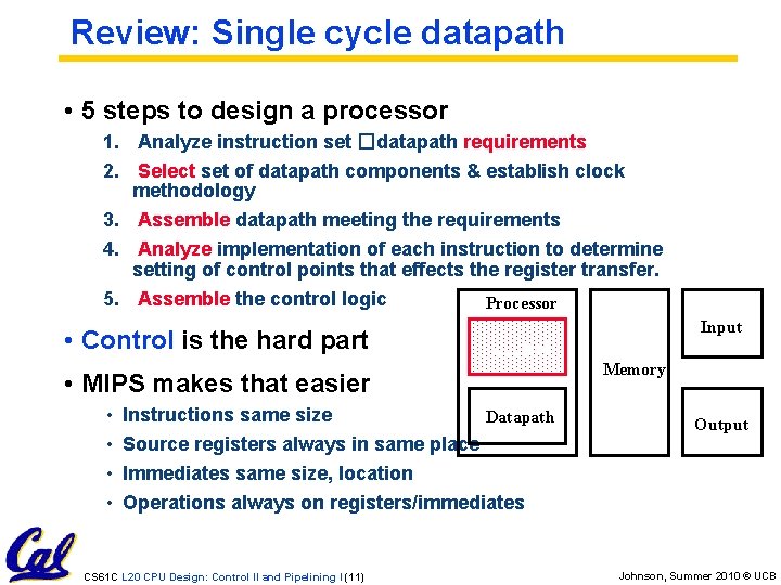
Review: Single cycle datapath • 5 steps to design a processor 1. Analyze instruction set �datapath requirements 2. Select set of datapath components & establish clock methodology 3. Assemble datapath meeting the requirements 4. Analyze implementation of each instruction to determine setting of control points that effects the register transfer. 5. Assemble the control logic Processor • Control is the hard part Input Control Memory • MIPS makes that easier • • Instructions same size Datapath Source registers always in same place Output Immediates same size, location Operations always on registers/immediates CS 61 C L 20 CPU Design: Control II and Pipelining I (11) Johnson, Summer 2010 © UCB
How We Build The Controller opcode func Reg. Dst = add + sub add ALUSrc = ori + lw + sw sub ori Memto. Reg = lw lw Reg. Write = add + sub + ori + lw “OR” logic “AND” logic sw Mem. Write = sw beq n. PCsel = beq jump Jump = jump Ext. Op = lw + sw ALUctr[0] = sub + beq (assume ALUctr is 0 ADD, 01: SUB, 10: OR) ALUctr[1] = or Reg. Dst ALUSrc Memto. Reg. Write Mem. Write n. PCsel Jump Ext. Op ALUctr[0] ALUctr[1] where, rtype = ~op 5 ~op 4 ~op 3 ~op 2 ori = ~op 5 ~op 4 op 3 op 2 lw = op 5 ~op 4 ~op 3 ~op 2 sw = op 5 ~op 4 op 3 ~op 2 beq = ~op 5 ~op 4 ~op 3 op 2 jump = ~op 5 ~op 4 ~op 3 ~op 2 ~op 1 ~op 0, ~op 1 op 0 ~op 1 ~op 0 Omigosh omigosh, do you know what this means? add = rtype func 5 ~func 4 ~func 3 ~func 2 ~func 1 ~func 0 sub = rtype func 5 ~func 4 ~func 3 ~func 2 func 1 ~func 0 CS 61 C L 20 CPU Design: Control II and Pipelining I (12) Johnson, Summer 2010 © UCB
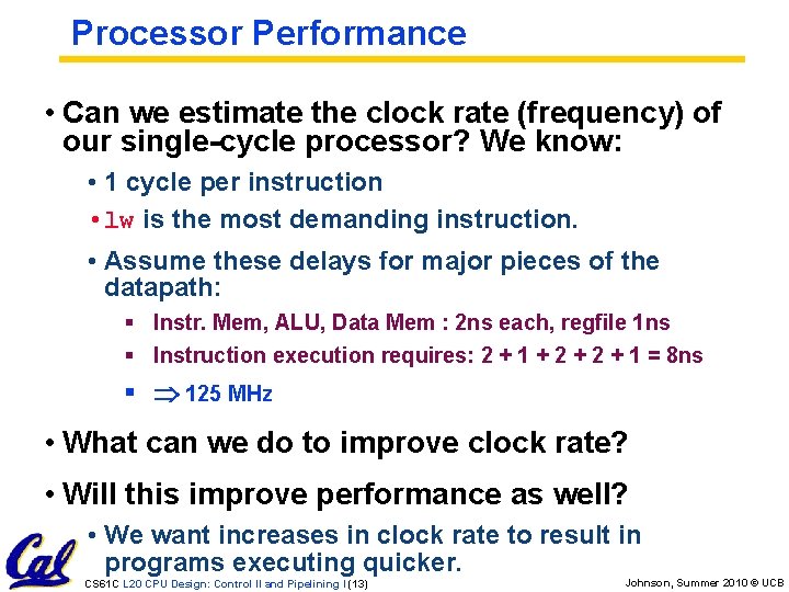
Processor Performance • Can we estimate the clock rate (frequency) of our single-cycle processor? We know: • 1 cycle per instruction • lw is the most demanding instruction. • Assume these delays for major pieces of the datapath: § Instr. Mem, ALU, Data Mem : 2 ns each, regfile 1 ns § Instruction execution requires: 2 + 1 + 2 + 1 = 8 ns § 125 MHz • What can we do to improve clock rate? • Will this improve performance as well? • We want increases in clock rate to result in programs executing quicker. CS 61 C L 20 CPU Design: Control II and Pipelining I (13) Johnson, Summer 2010 © UCB
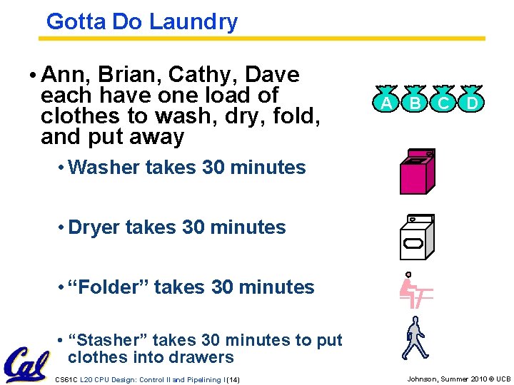
Gotta Do Laundry • Ann, Brian, Cathy, Dave each have one load of clothes to wash, dry, fold, and put away A B C D • Washer takes 30 minutes • Dryer takes 30 minutes • “Folder” takes 30 minutes • “Stasher” takes 30 minutes to put clothes into drawers CS 61 C L 20 CPU Design: Control II and Pipelining I (14) Johnson, Summer 2010 © UCB
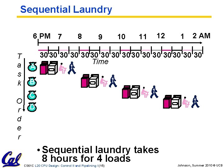
Sequential Laundry 6 PM 7 T a s k O r d e r A 8 9 10 11 12 1 2 AM 30 30 30 30 Time B C D • Sequential laundry takes 8 hours for 4 loads CS 61 C L 20 CPU Design: Control II and Pipelining I (15) Johnson, Summer 2010 © UCB
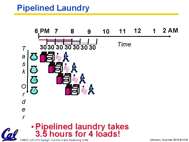
Pipelined Laundry 6 PM 7 T a s k 8 9 3030 30 30 10 11 12 1 2 AM Time A B C O D r d e r • Pipelined laundry takes 3. 5 hours for 4 loads! CS 61 C L 20 CPU Design: Control II and Pipelining I (16) Johnson, Summer 2010 © UCB
General Definitions • Latency: time to completely execute a certain task • for example, time to read a sector from disk is disk access time or disk latency • Throughput: amount of work that can be done over a period of time CS 61 C L 20 CPU Design: Control II and Pipelining I (17) Johnson, Summer 2010 © UCB
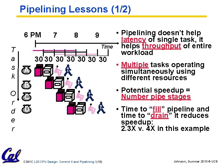
Pipelining Lessons (1/2) 6 PM T a s k 7 8 9 Time 30 30 A B O r d e r C D CS 61 C L 20 CPU Design: Control II and Pipelining I (18) • Pipelining doesn’t help latency of single task, it helps throughput of entire workload • Multiple tasks operating simultaneously using different resources • Potential speedup = Number pipe stages • Time to “fill” pipeline and time to “drain” it reduces speedup: 2. 3 X v. 4 X in this example Johnson, Summer 2010 © UCB
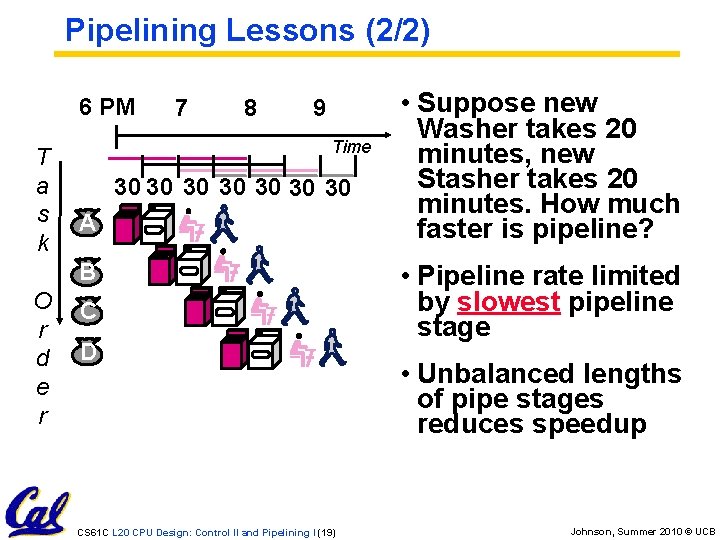
Pipelining Lessons (2/2) 6 PM T a s k 7 8 9 Time 30 30 A B O r d e r C D CS 61 C L 20 CPU Design: Control II and Pipelining I (19) • Suppose new Washer takes 20 minutes, new Stasher takes 20 minutes. How much faster is pipeline? • Pipeline rate limited by slowest pipeline stage • Unbalanced lengths of pipe stages reduces speedup Johnson, Summer 2010 © UCB
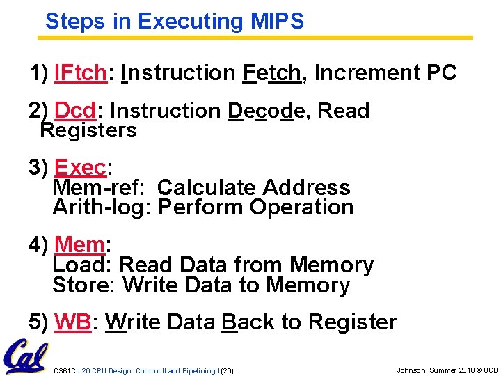
Steps in Executing MIPS 1) IFtch: Instruction Fetch, Increment PC 2) Dcd: Instruction Decode, Read Registers 3) Exec: Mem-ref: Calculate Address Arith-log: Perform Operation 4) Mem: Load: Read Data from Memory Store: Write Data to Memory 5) WB: Write Data Back to Register CS 61 C L 20 CPU Design: Control II and Pipelining I (20) Johnson, Summer 2010 © UCB
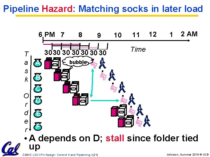
Pipeline Hazard: Matching socks in later load 6 PM 7 T a s k 8 9 3030 30 30 A 10 11 12 1 2 AM Time bubble B C O D r d E e r F • A depends on D; stall since folder tied up CS 61 C L 20 CPU Design: Control II and Pipelining I (21) Johnson, Summer 2010 © UCB
Administrivia • HW 8 due tomorrow • Project 2 due next Monday (parter • Newsgroup problems • Reminder: Midterm regrades due today CS 61 C L 20 CPU Design: Control II and Pipelining I (22) Johnson, Summer 2010 © UCB
Problems for Pipelining CPUs • Limits to pipelining: Hazards prevent next instruction from executing during its designated clock cycle • Structural hazards: HW cannot support some combination of instructions (single person to fold and put clothes away) • Control hazards: Pipelining of branches causes later instruction fetches to wait for the result of the branch • Data hazards: Instruction depends on result of prior instruction still in the pipeline (missing sock) • These might result in pipeline stalls or “bubbles” in the pipeline. CS 61 C L 20 CPU Design: Control II and Pipelining I (23) Johnson, Summer 2010 © UCB
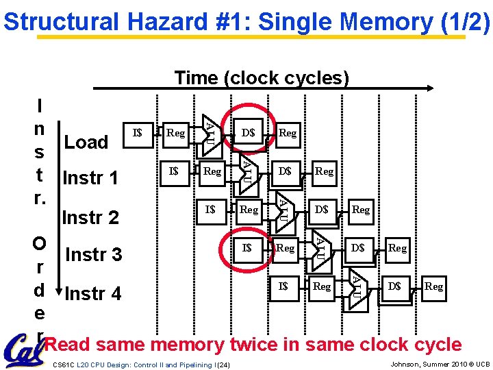
Structural Hazard #1: Single Memory (1/2) Time (clock cycles) ALU I n I$ D$ Reg s Load I$ D$ Reg t Instr 1 r. I$ D$ Reg Instr 2 O I$ D$ Reg Instr 3 r I$ D$ Reg d Instr 4 e r. Read same memory twice in same clock cycle ALU ALU CS 61 C L 20 CPU Design: Control II and Pipelining I (24) Johnson, Summer 2010 © UCB
Structural Hazard #1: Single Memory (2/2) • Solution: • infeasible and inefficient to create second memory • (We’ll learn about this more next week) • so simulate this by having two Level 1 Caches (a temporary smaller [of usually most recently used] copy of memory) • have both an L 1 Instruction Cache and an L 1 Data Cache • need more complex hardware to control when both caches miss CS 61 C L 20 CPU Design: Control II and Pipelining I (25) Johnson, Summer 2010 © UCB
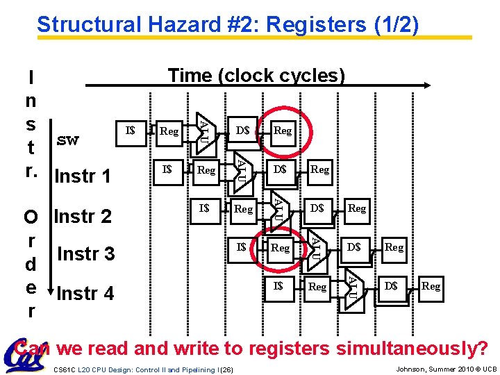
Structural Hazard #2: Registers (1/2) Reg D$ Reg I$ Reg ALU I$ D$ ALU Reg ALU I$ ALU O Instr 2 r Instr 3 d e Instr 4 r Time (clock cycles) ALU I n s t sw r. Instr 1 D$ Reg Can we read and write to registers simultaneously? CS 61 C L 20 CPU Design: Control II and Pipelining I (26) Johnson, Summer 2010 © UCB
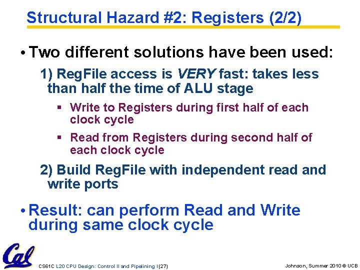
Structural Hazard #2: Registers (2/2) • Two different solutions have been used: 1) Reg. File access is VERY fast: takes less than half the time of ALU stage § Write to Registers during first half of each clock cycle § Read from Registers during second half of each clock cycle 2) Build Reg. File with independent read and write ports • Result: can perform Read and Write during same clock cycle CS 61 C L 20 CPU Design: Control II and Pipelining I (27) Johnson, Summer 2010 © UCB
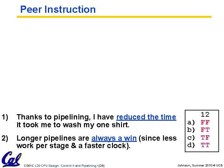
Peer Instruction 1) Thanks to pipelining, I have reduced the time it took me to wash my one shirt. 2) Longer pipelines are always a win (since less work per stage & a faster clock). CS 61 C L 20 CPU Design: Control II and Pipelining I (28) a) b) c) d) 12 FF FT TF TT Johnson, Summer 2010 © UCB
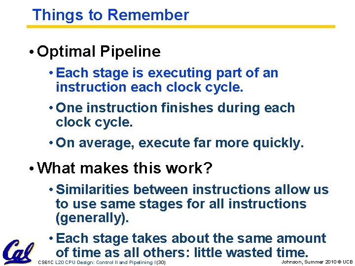
Things to Remember • Optimal Pipeline • Each stage is executing part of an instruction each clock cycle. • One instruction finishes during each clock cycle. • On average, execute far more quickly. • What makes this work? • Similarities between instructions allow us to use same stages for all instructions (generally). • Each stage takes about the same amount of time as all others: little wasted time. CS 61 C L 20 CPU Design: Control II and Pipelining I (30) Johnson, Summer 2010 © UCB

Bonus slides • These are extra slides that used to be included in lecture notes, but have been moved to this, the “bonus” area to serve as a supplement. • The slides will appear in the order they would have in the normal presentation CS 61 C L 20 CPU Design: Control II and Pipelining I (31) Johnson, Summer 2010 © UCB
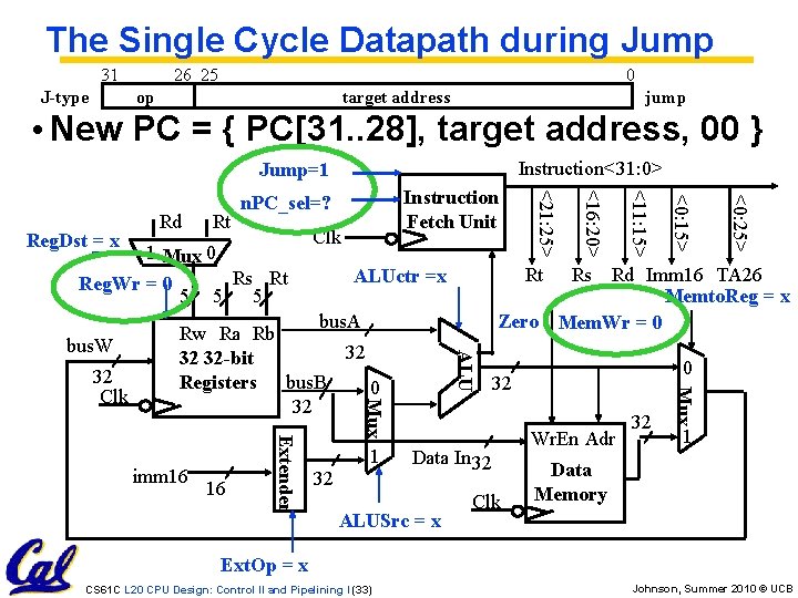
The Single Cycle Datapath during Jump 31 J-type 26 25 0 op jump target address • New PC = { PC[31. . 28], target address, 00 } Instruction<31: 0> Jump=1 <0: 25> Data In 32 ALUSrc = x 0 32 Clk Wr. En Adr 32 Mux 32 <0: 15> 1 <11: 15> 16 Extender imm 16 Rs Rd Imm 16 TA 26 Memto. Reg = x Zero Mem. Wr = 0 ALU bus. A Rw Ra Rb 32 32 32 -bit Registers bus. B 0 32 <16: 20> 5 Rt ALUctr =x Rs Rt 5 5 Mux 32 Clk 1 Mux 0 Reg. Wr = 0 bus. W Rt <21: 25> Reg. Dst = x Rd Instruction Fetch Unit n. PC_sel=? 1 Data Memory Ext. Op = x CS 61 C L 20 CPU Design: Control II and Pipelining I (33) Johnson, Summer 2010 © UCB
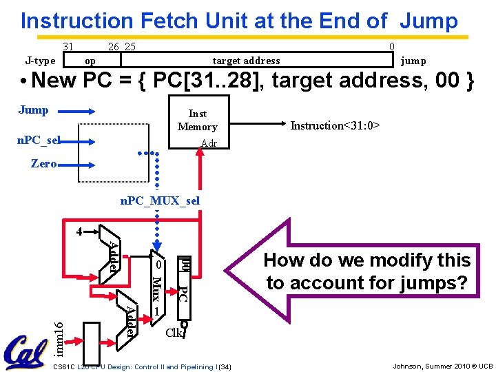
Instruction Fetch Unit at the End of Jump 31 26 25 J-type 0 op jump target address • New PC = { PC[31. . 28], target address, 00 } Jump Inst Memory n. PC_sel Instruction<31: 0> Adr Zero n. PC_MUX_sel Adder 0 PC Mux Adder imm 16 00 4 How do we modify this to account for jumps? 1 Clk CS 61 C L 20 CPU Design: Control II and Pipelining I (34) Johnson, Summer 2010 © UCB
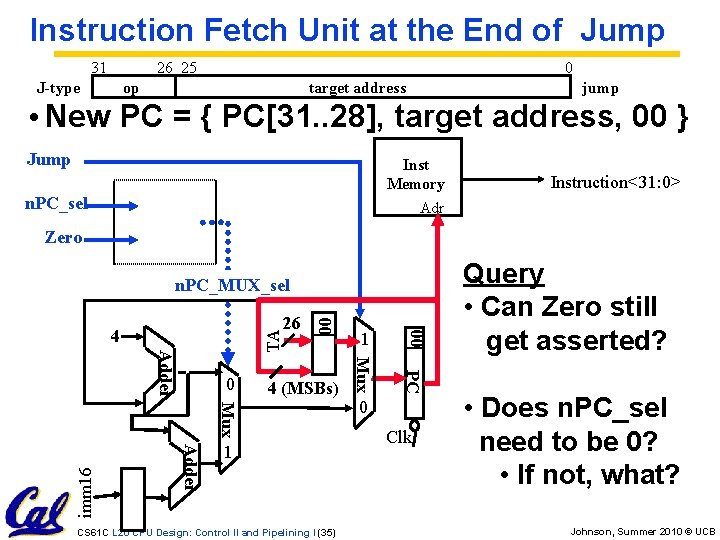
Instruction Fetch Unit at the End of Jump 31 26 25 J-type 0 op jump target address • New PC = { PC[31. . 28], target address, 00 } Jump Inst Memory n. PC_sel Instruction<31: 0> Adr Zero imm 16 Mux Adder 1 CS 61 C L 20 CPU Design: Control II and Pipelining I (35) 00 TA 4 (MSBs) 1 PC Adder 0 26 Mux 4 00 n. PC_MUX_sel 0 Clk Query • Can Zero still get asserted? • Does n. PC_sel need to be 0? • If not, what? Johnson, Summer 2010 © UCB
- Slides: 33