InputSpecific Dynamic Power Optimization for VLSI Circuits Fei

![Input-specific optimization Dominating path Can be [1, 41] 41 1 1 0 0 Why Input-specific optimization Dominating path Can be [1, 41] 41 1 1 0 0 Why](https://slidetodoc.com/presentation_image/5c706472e32224966db6a8af2d7b6081/image-15.jpg)


- Slides: 33

Input-Specific Dynamic Power Optimization for VLSI Circuits Fei Hu Intel Corp. Folsom, CA 95630, USA Vishwani D. Agrawal Department of ECE Auburn University, AL 36849, USA October 5, 2006

Outline Background – – Dynamic power dissipation Glitch reduction Previous LP model with fixed gate delay Process-variation-resistant LP model Input-specific optimization – Without process-variation – With process-variation Experimental results Conclusion Oct. 5, 2005 Fei Hu, ISLPED 2006, Tegernsee, Germany 2

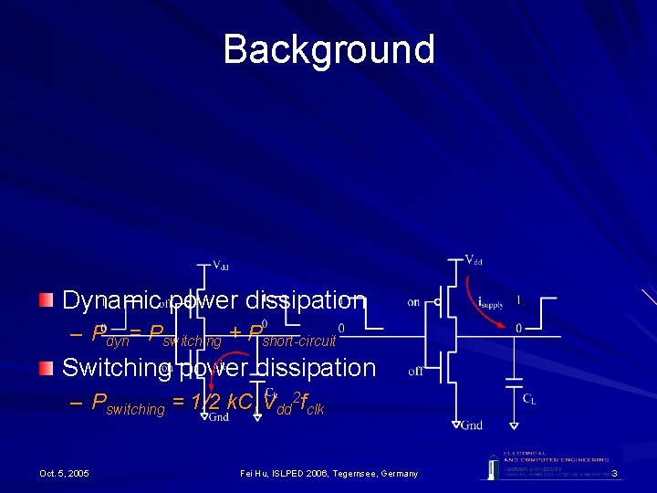
Background Dynamic power dissipation – Pdyn= Pswitching + Pshort-circuit Switching power dissipation – Pswitching = 1/2 k. CLVdd 2 fclk Oct. 5, 2005 Fei Hu, ISLPED 2006, Tegernsee, Germany 3

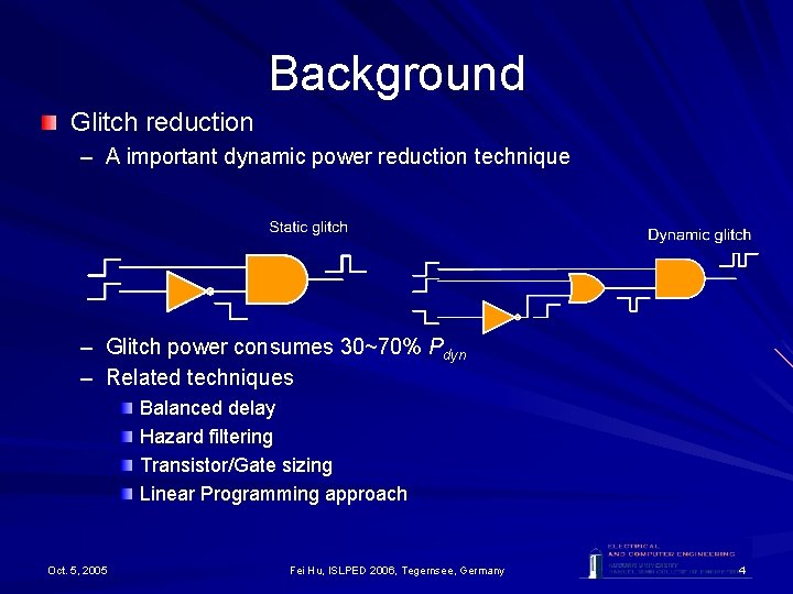
Background Glitch reduction – A important dynamic power reduction technique – Glitch power consumes 30~70% Pdyn – Related techniques Balanced delay Hazard filtering Transistor/Gate sizing Linear Programming approach Oct. 5, 2005 Fei Hu, ISLPED 2006, Tegernsee, Germany 4

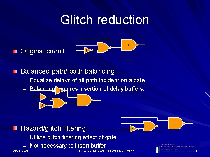
Glitch reduction Original circuit Balanced path/ path balancing – Equalize delays of all path incident on a gate – Balancing requires insertion of delay buffers. Hazard/glitch filtering – Utilize glitch filtering effect of gate – Not necessary to insert buffer Oct. 5, 2005 Fei Hu, ISLPED 2006, Tegernsee, Germany 5

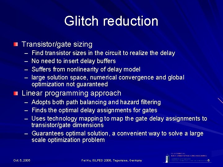
Glitch reduction Transistor/gate sizing – – Find transistor sizes in the circuit to realize the delay No need to insert delay buffers Suffers from nonlinearity of delay model large solution space, numerical convergence and global optimization not guaranteed Linear programming approach – Adopts both path balancing and hazard filtering – Finds the optimal delay assignments for gates – Uses technology mapping to map the gate delay assignments to transistor/gate dimensions – Guarantees optimal solution, a convenient way to solve a large scale optimization problem Oct. 5, 2005 Fei Hu, ISLPED 2006, Tegernsee, Germany 6

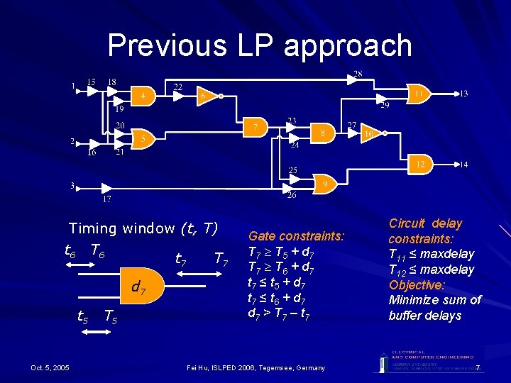
Previous LP approach Timing window (t, T) t 6 T 6 t 7 T 7 d 7 t 5 Oct. 5, 2005 T 5 Gate constraints: T 7 T 5 + d 7 T 7 T 6 + d 7 t 7 ≤ t 5 + d 7 t 7 ≤ t 6 + d 7 > T 7 – t 7 Fei Hu, ISLPED 2006, Tegernsee, Germany Circuit delay constraints: T 11 ≤ maxdelay T 12 ≤ maxdelay Objective: Minimize sum of buffer delays 7

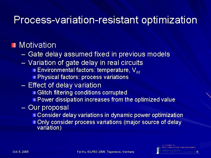
Process-variation-resistant optimization Motivation – Gate delay assumed fixed in previous models – Variation of gate delay in real circuits Environmental factors: temperature, Vdd Physical factors: process variations – Effect of delay variation Glitch filtering conditions corrupted Power dissipation increases from the optimized value – Our proposal Consider delay variations in dynamic power optimization Only consider process variations (major source of delay variation) Oct. 5, 2005 Fei Hu, ISLPED 2006, Tegernsee, Germany 8

LP model based on statistical timing Statistical timing model with random variables Oct. 5, 2005 Fei Hu, ISLPED 2006, Tegernsee, Germany 9

Outline Background – – Dynamic power dissipation Glitch reduction Previous LP model with fixed gate delay Process-variation-resistant LP model Input-specific optimization – Without process-variation – With process-variation Experimental results Conclusion Oct. 5, 2005 Fei Hu, ISLPED 2006, Tegernsee, Germany 10

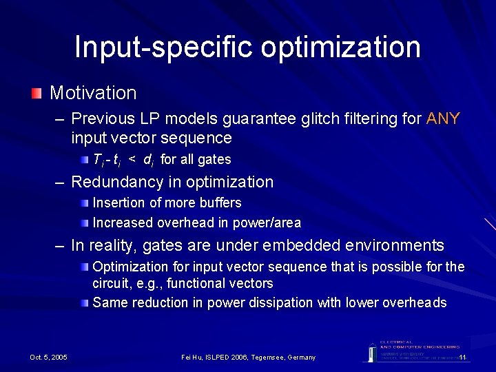
Input-specific optimization Motivation – Previous LP models guarantee glitch filtering for ANY input vector sequence Ti - ti < di for all gates – Redundancy in optimization Insertion of more buffers Increased overhead in power/area – In reality, gates are under embedded environments Optimization for input vector sequence that is possible for the circuit, e. g. , functional vectors Same reduction in power dissipation with lower overheads Oct. 5, 2005 Fei Hu, ISLPED 2006, Tegernsee, Germany 11

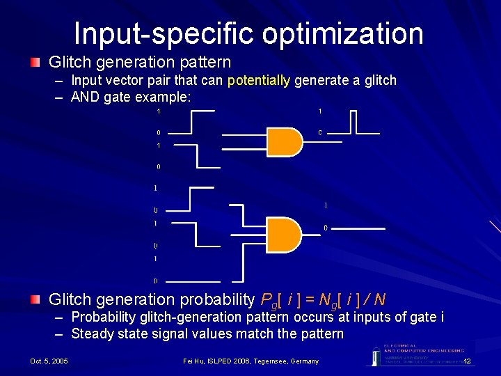
Input-specific optimization Glitch generation pattern – Input vector pair that can potentially generate a glitch – AND gate example: Glitch generation probability Pg[ i ] = Ng[ i ] / N – Probability glitch-generation pattern occurs at inputs of gate i – Steady state signal values match the pattern Oct. 5, 2005 Fei Hu, ISLPED 2006, Tegernsee, Germany 12

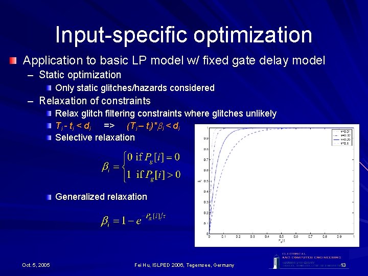
Input-specific optimization Application to basic LP model w/ fixed gate delay model – Static optimization Only static glitches/hazards considered – Relaxation of constraints Relax glitch filtering constraints where glitches unlikely Ti - ti < di => (Ti – ti)* i < di Selective relaxation Generalized relaxation Oct. 5, 2005 Fei Hu, ISLPED 2006, Tegernsee, Germany 13

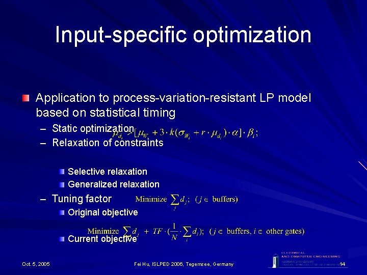
Input-specific optimization Application to process-variation-resistant LP model based on statistical timing – Static optimization – Relaxation of constraints Selective relaxation Generalized relaxation – Tuning factor Original objective Current objective Oct. 5, 2005 Fei Hu, ISLPED 2006, Tegernsee, Germany 14
![Inputspecific optimization Dominating path Can be 1 41 41 1 1 0 0 Why Input-specific optimization Dominating path Can be [1, 41] 41 1 1 0 0 Why](https://slidetodoc.com/presentation_image/5c706472e32224966db6a8af2d7b6081/image-15.jpg)
Input-specific optimization Dominating path Can be [1, 41] 41 1 1 0 0 Why do we need a tuning factor 1 1 – Dominating path affects critical delay distribution Oct. 5, 2005 Fei Hu, ISLPED 2006, Tegernsee, Germany 15

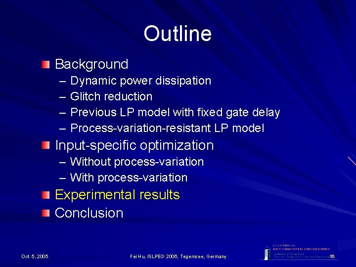
Outline Background – – Dynamic power dissipation Glitch reduction Previous LP model with fixed gate delay Process-variation-resistant LP model Input-specific optimization – Without process-variation – With process-variation Experimental results Conclusion Oct. 5, 2005 Fei Hu, ISLPED 2006, Tegernsee, Germany 16

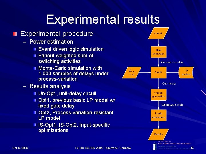
Experimental results Experimental procedure – Power estimation Event driven logic simulation Fanout weighted sum of switching activities Monte-Carlo simulation with 1, 000 samples of delays under process-variation – Results analysis Un-Opt. , unit-delay circuit Opt 1, previous basic LP model w/ fixed gate delay Opt 2, Process-variation-resistant LP model IS-Opt 1, IS-Opt 2, Input-specific optimizations Oct. 5, 2005 Fei Hu, ISLPED 2006, Tegernsee, Germany 17

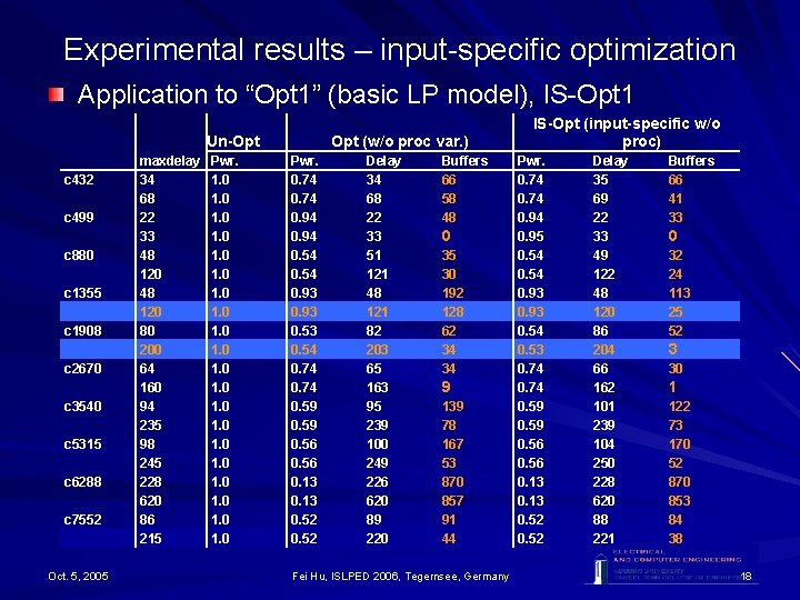
Experimental results – input-specific optimization Application to “Opt 1” (basic LP model), IS-Opt 1 Un-Opt c 432 c 499 c 880 c 1355 c 1908 c 2670 c 3540 c 5315 c 6288 c 7552 Oct. 5, 2005 maxdelay 34 68 22 33 48 120 80 200 64 160 94 235 98 245 228 620 86 215 Pwr. 1. 0 1. 0 Opt (w/o proc var. ) Pwr. 0. 74 0. 94 0. 54 0. 93 0. 53 0. 54 0. 74 0. 59 0. 56 0. 13 0. 52 Delay 34 68 22 33 51 121 48 121 82 203 65 163 95 239 100 249 226 620 89 220 Buffers 66 58 48 0 35 30 192 128 62 34 34 9 139 78 167 53 870 857 91 44 Fei Hu, ISLPED 2006, Tegernsee, Germany IS-Opt (input-specific w/o proc) Pwr. 0. 74 0. 94 0. 95 0. 54 0. 93 0. 54 0. 53 0. 74 0. 59 0. 56 0. 13 0. 52 Delay 35 69 22 33 49 122 48 120 86 204 66 162 101 239 104 250 228 620 88 221 Buffers 66 41 33 0 32 24 113 25 52 3 30 1 122 73 170 52 870 853 84 38 18

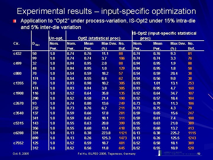
Experimental results – input-specific optimization Application to “Opt 2” under process-variation, IS-Opt 2 under 15% intra-die and 5% inter-die variation Un-opt. Cir. DMax c 432 50 99 32 48 70 174 116 290 93 232 137 341 143 356 331 899 125 312 c 499 c 880 c 1355 c 1908 c 2670 c 3540 c 5315 c 6288 c 7552 Oct. 5, 2005 Nom. Pwr. 1. 0 1. 0 Opt 2 (statistical proc) Nom. Pwr. 0. 74 0. 94 0. 54 0. 93 0. 52 0. 74 0. 73 0. 59 0. 55 0. 13 0. 52 Mean Pwr. 0. 76 0. 74 0. 95 0. 59 0. 55 0. 98 0. 94 0. 64 0. 58 0. 80 0. 76 0. 62 0. 63 0. 60 0. 38 0. 26 0. 59 0. 56 Max Dev. (%) 11. 1 3. 7 2. 0 18. 2 8. 6 10. 2 3. 0 35. 8 21. 4 13. 6 6. 2 17. 8 10. 1 20. 8 13. 4 223. 8 125. 3 18. 7 11. 8 No. Buf. 88 106 88 129 57 62 305 135 190 249 211 281 311 399 418 1121 1473 481 645 IS-Opt 2 (input-specific statistical proc) Nom. Pwr. 0. 74 0. 94 0. 54 0. 93 0. 52 0. 73 0. 59 0. 55 0. 13 0. 52 Fei Hu, ISLPED 2006, Tegernsee, Germany Mean Pwr. 0. 76 0. 74 0. 95 0. 59 0. 56 1. 01 0. 95 0. 64 0. 57 0. 79 0. 75 0. 61 0. 63 0. 60 0. 38 0. 26 0. 58 0. 55 Max Dev. (%) 9. 3 3. 3 1. 9 1. 8 20. 4 9. 0 13. 1 4. 7 34. 7 18. 4 11. 3 4. 3 15. 6 7. 4 21. 0 13. 2 225. 2 125. 5 18. 1 10. 9 No. Buf. 81 76 88 58 38 38 253 160 107 104 186 79 247 188 389 413 1115 1243 389 520 19

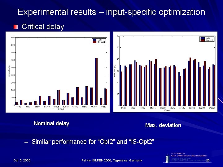
Experimental results – input-specific optimization Critical delay Nominal delay Max. deviation – Similar performance for “Opt 2” and “IS-Opt 2” Oct. 5, 2005 Fei Hu, ISLPED 2006, Tegernsee, Germany 20

Outline Background – – Dynamic power dissipation Glitch reduction Previous LP model with fixed gate delay Process-variation-resistant LP model Input-specific optimization – Without process-variation – With process-variation Experimental results Conclusion Oct. 5, 2005 Fei Hu, ISLPED 2006, Tegernsee, Germany 21

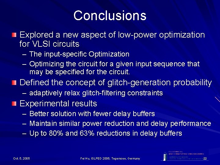
Conclusions Explored a new aspect of low-power optimization for VLSI circuits – The input-specific Optimization – Optimizing the circuit for a given input sequence that may be specified for the circuit. Defined the concept of glitch-generation probability – adaptively relax glitch-filtering constraints Experimental results – Better solution with fewer delay buffers – Maintain similar power reduction and delay performance – Up to 80% and 63% reductions in delay buffers Oct. 5, 2005 Fei Hu, ISLPED 2006, Tegernsee, Germany 22

Q&A Oct. 5, 2005 Fei Hu, ISLPED 2006, Tegernsee, Germany 23

Backups

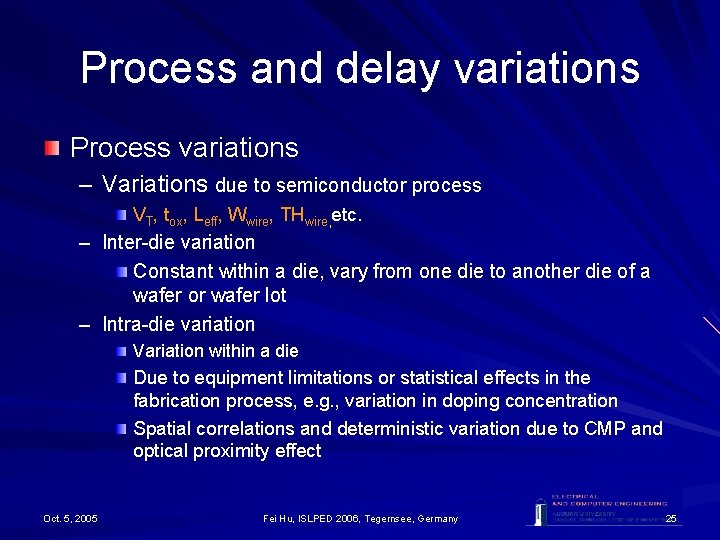
Process and delay variations Process variations – Variations due to semiconductor process VT, tox, Leff, Wwire, THwire, etc. – Inter-die variation Constant within a die, vary from one die to another die of a wafer or wafer lot – Intra-die variation Variation within a die Due to equipment limitations or statistical effects in the fabrication process, e. g. , variation in doping concentration Spatial correlations and deterministic variation due to CMP and optical proximity effect Oct. 5, 2005 Fei Hu, ISLPED 2006, Tegernsee, Germany 25

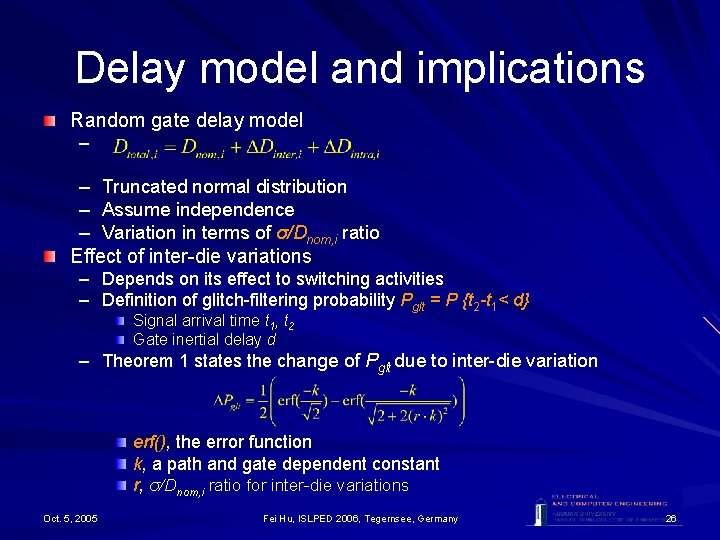
Delay model and implications Random gate delay model – – Truncated normal distribution – Assume independence – Variation in terms of σ/Dnom, i ratio Effect of inter-die variations – Depends on its effect to switching activities – Definition of glitch-filtering probability Pglt = P {t 2 -t 1< d} Signal arrival time t 1, t 2 Gate inertial delay d – Theorem 1 states the change of Pglt due to inter-die variation erf(), the error function k, a path and gate dependent constant r, σ/Dnom, i ratio for inter-die variations Oct. 5, 2005 Fei Hu, ISLPED 2006, Tegernsee, Germany 26

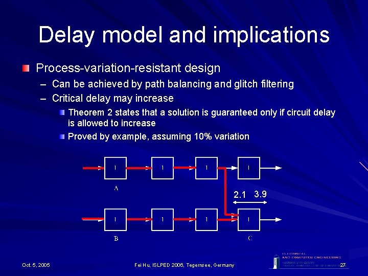
Delay model and implications Process-variation-resistant design – Can be achieved by path balancing and glitch filtering – Critical delay may increase Theorem 2 states that a solution is guaranteed only if circuit delay is allowed to increase Proved by example, assuming 10% variation 2. 1 3. 9 Oct. 5, 2005 Fei Hu, ISLPED 2006, Tegernsee, Germany 27

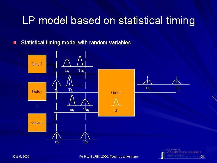
LP model based on statistical timing Statistical timing model with random variables Oct. 5, 2005 Fei Hu, ISLPED 2006, Tegernsee, Germany 28

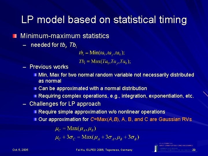
LP model based on statistical timing Minimum-maximum statistics – needed for tbi, Tbi – Previous works Min, Max for two normal random variable not necessarily distributed as normal Can be approximated with a normal distribution Requiring complex operations, e. g. , integration, exponentiation, etc. – Challenges for LP approach Require simple approximation w/o nonlinear operations Our approximation for C=Max(A, B), A, B, and C are Gaussian RVs Oct. 5, 2005 Fei Hu, ISLPED 2006, Tegernsee, Germany 29

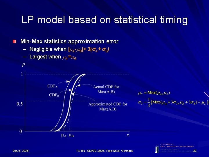
LP model based on statistical timing Min-Max statistics approximation error – Negligible when | A- B|> 3(σA+ σB) – Largest when A= B Oct. 5, 2005 Fei Hu, ISLPED 2006, Tegernsee, Germany 30

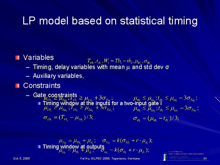
LP model based on statistical timing Variables – Timing, delay variables with mean and std dev σ – Auxiliary variables, Constraints – Gate constraints Timing window at the inputs for a two-input gate i Timing window at outputs Oct. 5, 2005 Fei Hu, ISLPED 2006, Tegernsee, Germany 31

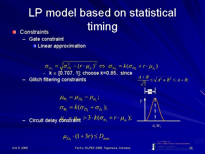
LP model based on statistical timing Constraints – Gate constraint Linear approximation – k [0. 707, 1]; choose k=0. 85, since – Glitch filtering constraints – Circuit delay constraint Oct. 5, 2005 Fei Hu, ISLPED 2006, Tegernsee, Germany 32

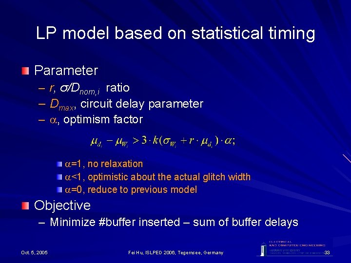
LP model based on statistical timing Parameter – r, σ/Dnom, i ratio – Dmax, circuit delay parameter – , optimism factor =1, no relaxation <1, optimistic about the actual glitch width =0, reduce to previous model Objective – Minimize #buffer inserted – sum of buffer delays Oct. 5, 2005 Fei Hu, ISLPED 2006, Tegernsee, Germany 33