Input common mode range drop VDD VDS 3


- Slides: 25

Input common mode range drop VDD – VDS 3 sat + VT 1 > vicm > VDS 5 sat + VT 1 + Von 1 1. 25 -0. 125 + 0. 75 > vicm > 0. 125+0. 75+0. 125, unsymmetric!

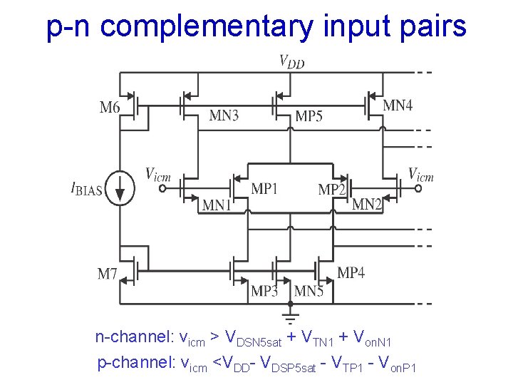
p-n complementary input pairs n-channel: vicm > VDSN 5 sat + VTN 1 + Von. N 1 p-channel: vicm <VDD- VDSP 5 sat - VTP 1 - Von. P 1

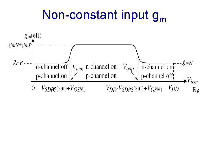
Non-constant input gm N

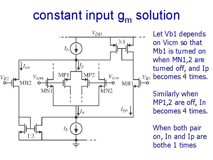
constant input gm solution Let Vb 1 depends on Vicm so that Mb 1 is turned on when MN 1, 2 are turned off, and Ip becomes 4 times. Similarly when MP 1, 2 are off, In becomes 4 times. When both pair on, In and Ip are bothe 1 times

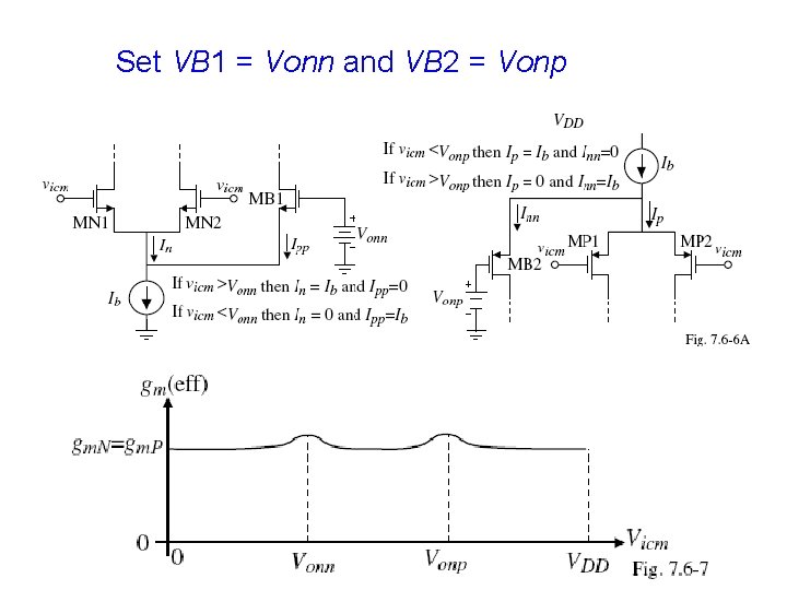
Set VB 1 = Vonn and VB 2 = Vonp

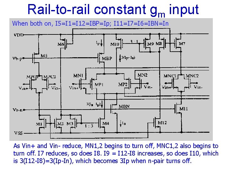
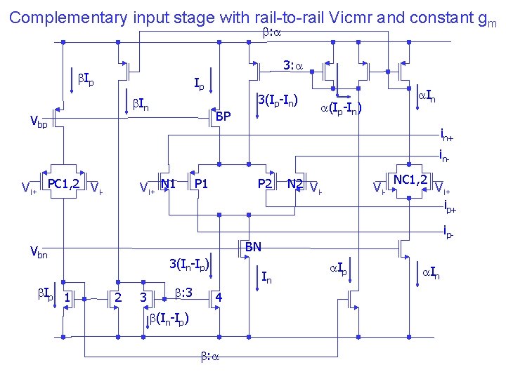
Rail-to-rail constant gm input When both on, I 5=I 12=IBP=Ip; I 11=I 7=I 6=IBN=In As Vin+ and Vin- reduce, MN 1, 2 begins to turn off, MNC 1, 2 also begins to turn off. I 7 reduces, so does I 8. I 9 = I 12 -I 8 increases, so does I 10, which is 3(I 12 -I 8)=3(Ip-In), which becomes 3 Ip when n-pair turns off.

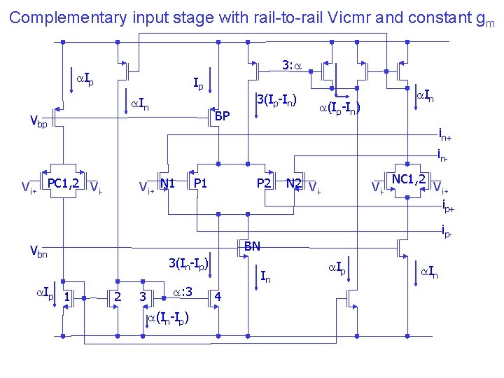
Complementary input stage with rail-to-rail Vicmr and constant gm 3: a a. Ip Ip a. In Vbp BP 3(Ip-In) a. In a(Ip-In) in+ in- Vi+ PC 1, 2 Vi- Vi+ N 1 P 2 N 2 V i- Vi- NC 1, 2 Vi+ ip- BN Vbn a. Ip 1 P 1 3(In-Ip) 2 3 a: 3 a(In-Ip) In 4 a. Ip a. In

Complementary input stage with rail-to-rail Vicmr and constant gm b: a 3: a b. Ip Ip b. In Vbp BP 3(Ip-In) a. In a(Ip-In) in+ in- Vi+ PC 1, 2 Vi- Vi+ N 1 P 2 N 2 V i- Vi- NC 1, 2 Vi+ ip- BN Vbn b. Ip 1 P 1 3(In-Ip) 2 3 b: 3 In 4 b(In-Ip) b: a a. Ip a. In

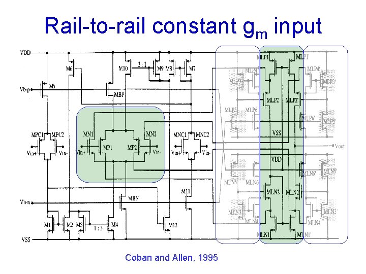
Rail-to-rail constant gm input Coban and Allen, 1995

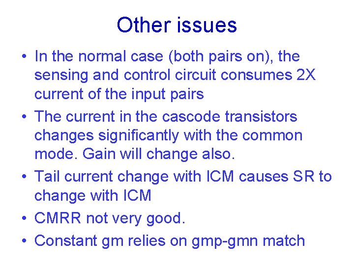
Other issues • In the normal case (both pairs on), the sensing and control circuit consumes 2 X current of the input pairs • The current in the cascode transistors changes significantly with the common mode. Gain will change also. • Tail current change with ICM causes SR to change with ICM • CMRR not very good. • Constant gm relies on gmp-gmn match

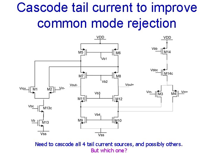
Cascode tail current to improve common mode rejection Need to cascode all 4 tail current sources, and possibly others. But which one?

Complementary input stage with rail-to-rail Vicmr and constant gm b: a 3: a b. Ip Ip b. In Vbp BP 3(Ip-In) a. In a(Ip-In) in+ in- Vi+ PC 1, 2 Vi- Vi+ N 1 P 2 N 2 V i- Vi- NC 1, 2 Vi+ ip- BN Vbn b. Ip 1 P 1 3(In-Ip) 2 3 b: 3 In 4 b(In-Ip) b: a a. Ip a. In

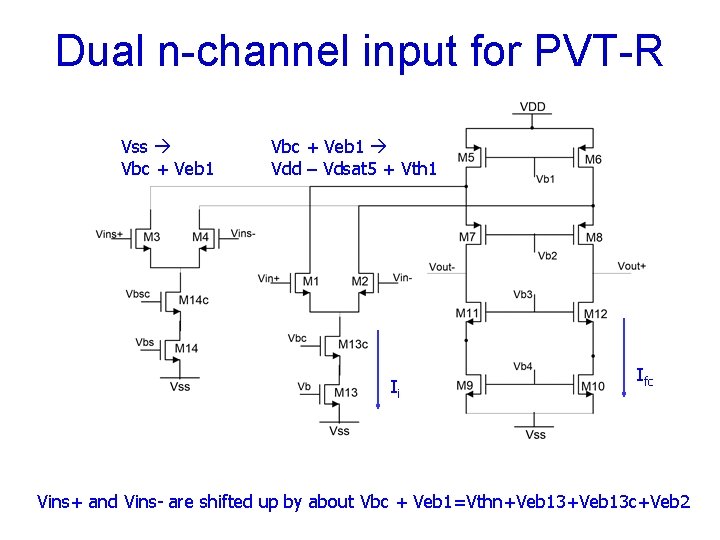
Dual n-channel input for PVT-R Vss Vbc + Veb 1 Vdd – Vdsat 5 + Vth 1 Ii Ifc Vins+ and Vins- are shifted up by about Vbc + Veb 1=Vthn+Veb 13 c+Veb 2

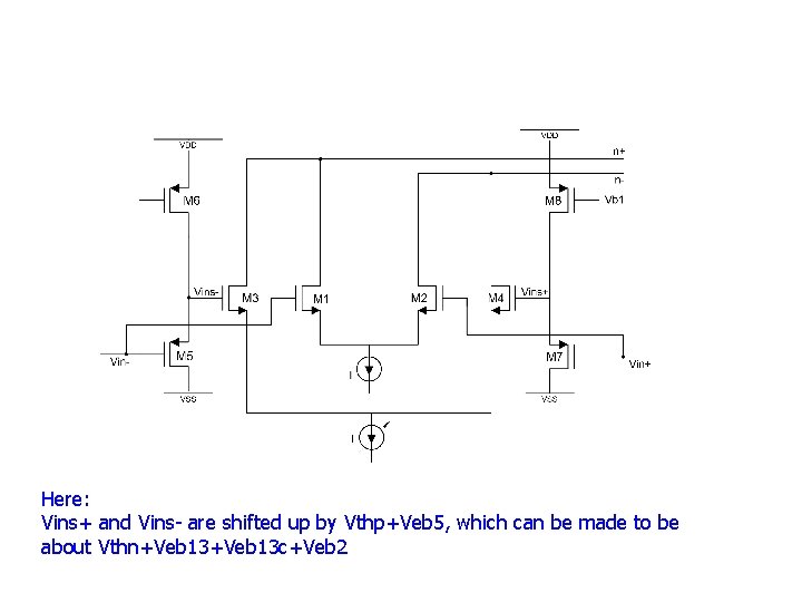
Here: Vins+ and Vins- are shifted up by Vthp+Veb 5, which can be made to be about Vthn+Veb 13 c+Veb 2

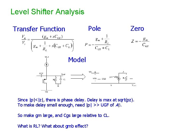
Level Shifter Analysis Pole Transfer Function Zero Model Since |p|<|z|, there is phase delay. Delay is max at sqrt(pz). To make delay small enough, need |p| >> UGF of Ab. So make gm large, and Cgs large relative to CL. What is RL? What about gmb effect?

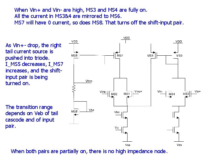
When Vin+ and Vin- are high, MS 3 and MS 4 are fully on. All the current in MS 3&4 are mirrored to MS 6. MS 7 will have 0 current, so does MS 8. That turns off the shift-input pair. As Vin+- drop, the right tail current source is pushed into triode. I_MS 5 decreases, I_MS 7 increases, and the shiftinput pair is being turned on. The transition range depends on Veb of tail cascode and of input pair. When both pairs are partially on, there is no high impedance node.

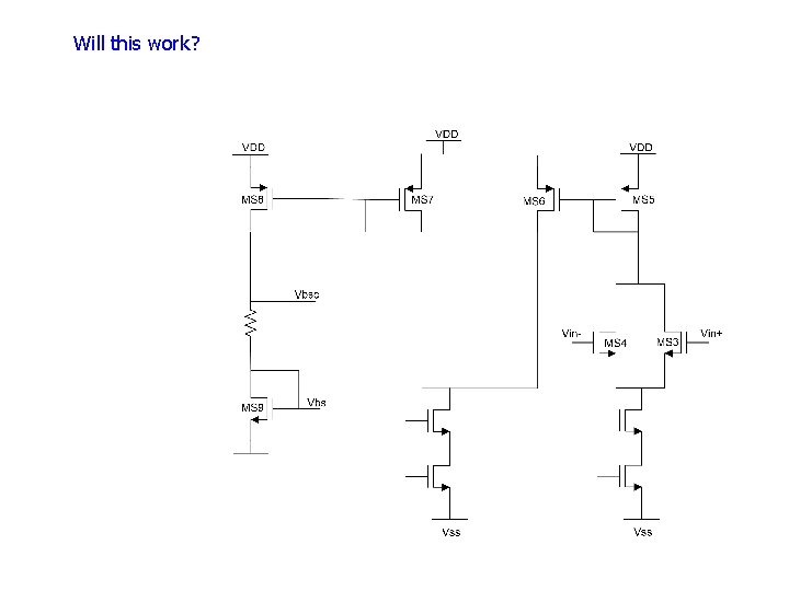
Will this work?

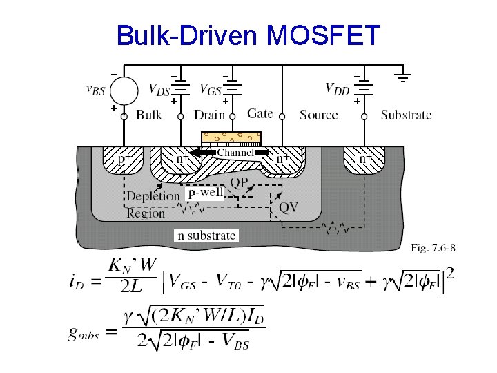
Bulk-Driven MOSFET

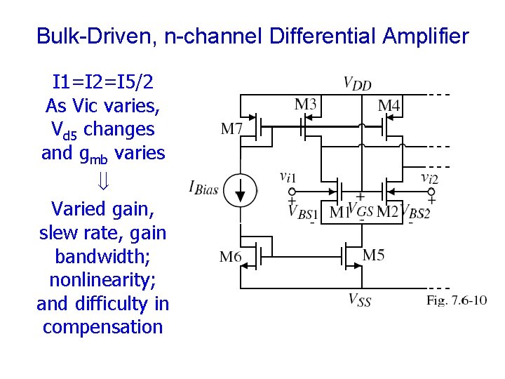
Bulk-Driven, n-channel Differential Amplifier I 1=I 2=I 5/2 As Vic varies, Vd 5 changes and gmb varies Varied gain, slew rate, gain bandwidth; nonlinearity; and difficulty in compensation

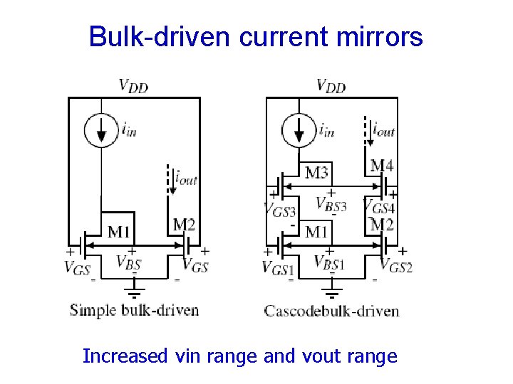
Bulk-driven current mirrors Increased vin range and vout range

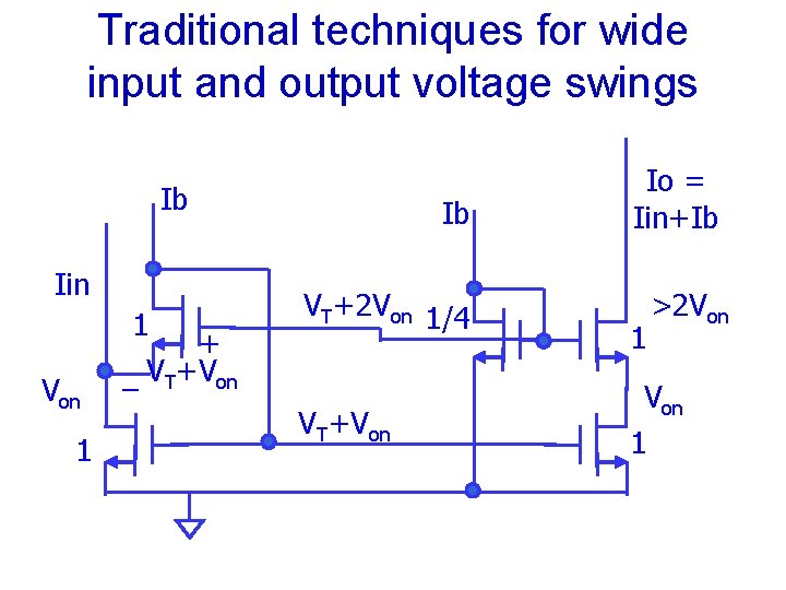
Traditional techniques for wide input and output voltage swings Ib Iin Von 1 1 + VT+Von – Ib VT+2 Von 1/4 VT+Von Io = Iin+Ib 1 >2 Von 1

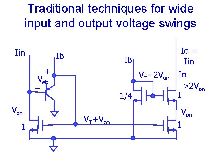
Traditional techniques for wide input and output voltage swings Iin Ib Ib + VT+2 Von Veb – Von 1 Io = Iin 1/4 VT+Von Io >2 Von 1

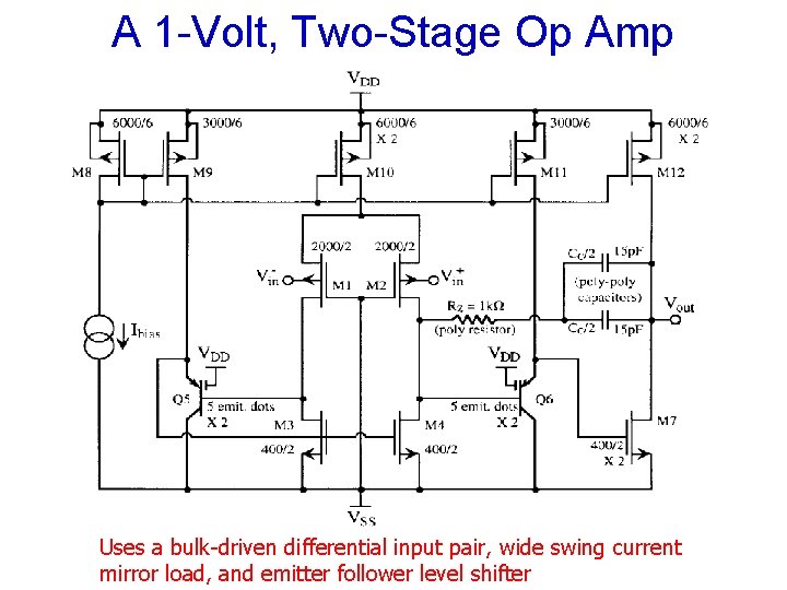
A 1 -Volt, Two-Stage Op Amp Uses a bulk-driven differential input pair, wide swing current mirror load, and emitter follower level shifter

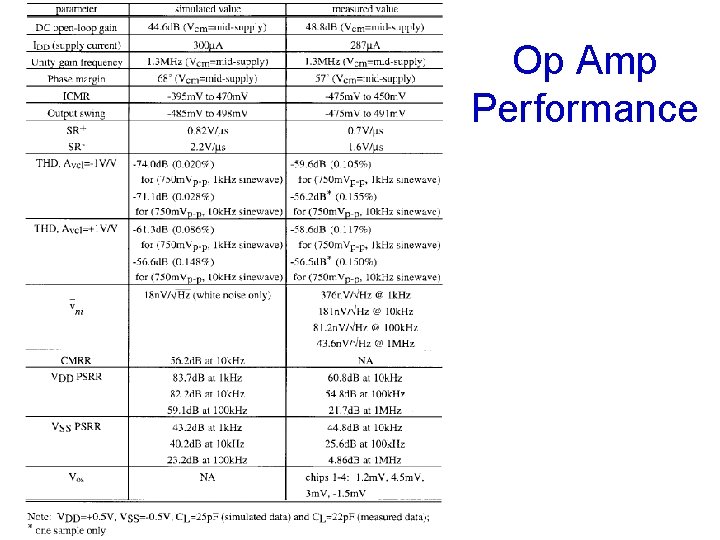
Op Amp Performance

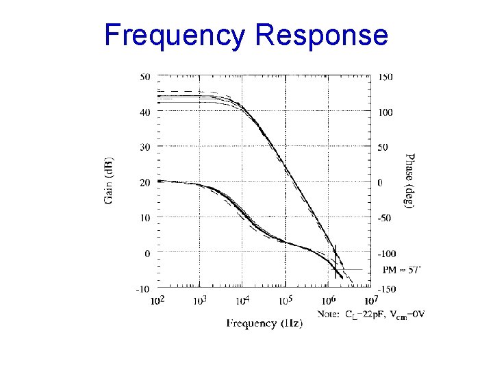
Frequency Response