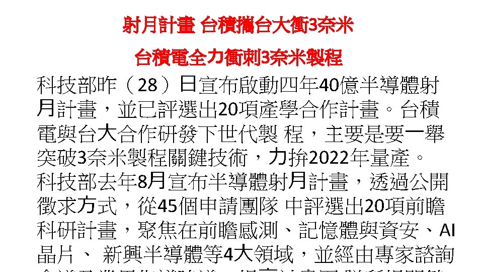
Innovations Enabling Semiconductor Roadmap Chee Wee Liu cliuntu
 cliu@ntu. edu. tw http: //www. nanosioe.")
Innovations Enabling Semiconductor Roadmap Chee Wee Liu (劉致為) cliu@ntu. edu. tw http: //www. nanosioe. ee. ntu. edu. tw High mobility/High K/ 3 D x 3 D GDP similar to Philippine (1. 2 x) if semi dies 23 M vs 1. 3 B Profile of graduate students and postdoc Professor: 6+ 3 TSMC/MTK/GF/Intel/UMC/VG/SMIC: 100+ (best is Director) Graduate admission(2017) Berkeley, MIT… 1

2017 年全球半導體廠商營收前十大排名 2017 Rank 2016 Rank 1 2 2 3 1 4 4 6 5 6 3 5 7 7 8 Source: Gartner (January 2018) 2017 Revenue 61, 215 14. 6 40, 104 52. 6 57, 712 26, 309 13. 8 6. 3 54, 091 14, 700 6. 7 79. 0 23, 062 5. 5 12, 950 78. 1 17, 063 15, 490 4. 1 3. 7 15, 415 13, 223 10. 7 17. 1 13, 806 3. 3 11, 901 16. 0 8 Vendor Samsung Electronics Intel SK Hynix Micron Technology Qualcomm Broadcom Texas Instruments Toshiba 2017 Market Share (%) 2016 Revenue 2016 -2017 Growth (%) 12, 813 3. 1 9, 918 29. 2 9 17 Western Digital 9, 181 2. 2 4, 170 120. 2 10 9 NXP Others 8, 651 174, 418 2. 1 41. 6 9, 306 157, 736 -7. 0 10. 6 Total Market 419, 720 100. 0 343, 514 3 00

4

5

The top eight transformative technologies for the global technology market in 2018, IHS Markt report Ref: https: //www. businesswire. com/news/home/20180104005040/en/IHS-Markit-Identifies-Top-Technology-Trends-2018 Digital current : BITCOIN IOT AI Blockchain Cloud AI On-Device AI Cloud and Virtualization 2018 Technology trend Connectivity 5 G wireless Ubiquitous video Broadcast Robot and Drone Computer vision Image sensor Image processing and analysis 6

Strained Si starting from 90 nm node • Enabling technologies: high mobility, high-k/metal gate, 3 D transistor 7

8

TSMC’s Roadmap 5/2/2018 https: //www. eetimes. com/document. asp? doc_id=1333244&print=yes u 7 nm: 2018/5 in volume production u 7 nm+:early 2019, using EUV lithography ramping u 5 nm: • To start risk production of a 5 -nm node in the first half of 2019. • To use EUV on multiple layers and 5 -nm nodes. • To start 5 -nm production in 2020. u 2 nm and beyond: • Stacked nanowires or nanosheets • Germanium channel with record-low contact resistance • 2 D back-end materials including molybdenum disulfide • To enlarge copper grains to reduce resistance in interconnects. • selective dielectric-on-dielectric deposition process to enable self-aligning of copper vias. 9
 • Unit cell of silicon crystal")
Silicon Crystal Structure (Ge, Si. Ge, Ge. Sn) • Unit cell of silicon crystal is cubic. • Each Si atom has 4 nearest neighbors. • Si sp 3 10

Large Ion and small Vdd • 要馬兒好又要馬兒不吃草 11

12

13

Power Saving : To Increase Mobility 14
 in transistor level small VDD log ID")
Reduce to Power (= CVDD 2 f) in transistor level small VDD log ID Ion Small SS Large SS Delay = CV/Ion SS (subthreshold slope) = inverse of the slope in log ID vs VG plot Ioff VDD(0. 5 V) VDD(0. 9 V) VG • SS ≥ 60 m. V/decade for thermionic emission • SS ≤ 60 m. V/decade → NCFET , TFET 15
 • Intel co-founder Gorden Moore noticed in 1964 • Transistor")
Moore’s Law (scaled FETs) • Intel co-founder Gorden Moore noticed in 1964 • Transistor density on a chip doubles per generation • Amazingly still correct, likely to keep until 20 xx MORE Than MOORE: Sensor/MEMS, Analog, RF, … 16
 Δ 2 Strained Si Δ 4 Mobility")
Strained Si at room temperature (90 nm) Δ 2 Strained Si Δ 4 Mobility enhancement Control Si M. H. Lee et al. , IEDM, 69 (2003). The tensile strain lowers Δ 2 valleys with low in-plane effective mass. l More electron in high mobility Δ 2 valleys l ~2 x enhancement l 17

High mobility strained Si Si. Ge barrier layer Si QW modulation doped layer 2 D electrons Si. Ge relaxed buffer layer µ~3. 5 x 105 cm 2/V-s Ref: F. Schaffler et al. , Semicond. Sci. Tech. , 12, 1515 (1997). l Our approach To reduce Coulomb scattering: 1. No doping heterostructure. in the Si. Ge/Si/Si. Ge 2. Thick Si. Ge barrier layer. To prevent remote charged impurity scattering from gate stack l To reduce phonon scattering: 2 DEG mobility is measured at 0. 3 K. 18

Si. Ge Graded Buffer Layers Si. Ge relaxed buffer Si. Ge graded buffer Si. Ge barrier layer 1μm l • 200 nm Si QW Step graded buffer layer Dislocations confined in the compositionally graded buffer layer. 19

Quantum Hall Effect 1. 6 M cm 2/V-s T. M. Lu et al. , APL, 94, 182102 (2009). Collaborate with Prof. D. C. Tsui, Princeton Univ. l Integral and fraction quantum Hall Effect can is observed in the 2 DEG structure. 20
 Background charges: 1.")
Record High 2 DEG Mobility (2. 4 M cm 2/V s) Background charges: 1. 2 x 1014 cm-3 20% enhancement Background charges: 2. 3 x 1014 cm-3 M. Yu. Melnikov et al. , APL, 106, 092102 (2015). Collaborate with Prof. S. V. Kravchenko, Northeastern Univ. l 2. 4 × 106 cm 2/V s by the reduction of background charges from 2. 3 x 1014 cm-3 to 1. 2 x 1014 cm-3. 21

MRS Bulletin Aug. 2014 • Si. Ge/Ge has higher mobility than Si • Ge. Sn mobility is not known! 22

Si. Ge channel PFET using Si cap Si 0. 2 Ge 0. 8 Si • Si cap for high K/metal gate • 3 x mobility enhancement C. Y. Peng APL 2007, ROC patent 2006 23

Strained Si 0. 75 Ge 0. 25 channel p. FET • A substantial improvement of 70– 85 % with Si. Ge fins is noticed at high carrier density of 1013 cm− 2. Ref: Toward Quantum Fin. FET pp 55 -79 24

25

Effects of High-k • k ↑, Cox, inv ↑, Ion ↑ • k ↑, thigh-k ↑, leakage ↓ 26

27
 Feature Dimension Ti. N layer")
Intel 22 nm : Gate stack of PMOS (high-k) Feature Dimension Ti. N layer above Hf. O 2 1 nm Ta. Al barrier 1 nm Ti. N work function metal 4 nm Al. CO layer 3. 5 nm Ti. Al. N layer 2. 5 nm W gate fill 6 nm • Rounded silicon fins are 18 nm thick at foot, 7 nm thick at fin top. Ti. N is used to prevent W diffusing. • Work function metal of PMOS is Ti. N/Al. CO/Ti. Al. N. • Gate dielectric of PMOS is Si. O(0. 6 nm)/Hf. O 2(2 nm). 28
 Feature Dimension Ti. N layer")
Intel 22 nm : Gate stack of NMOS (high-k) Feature Dimension Ti. N layer above Hf. O 2 1 nm Ta. Al barrier 1 nm Al. Ti. CO work function metal 2. 9 nm Ti. N layer 2. 6 nm W gate fill 6 nm • Rounded silicon fins are 18 nm thick at foot, 7 nm thick at fin top. Ti. N is used to prevent W diffusing. • Work function metal of NMOS is Al. Ti. CO/Ti. N. • Gate dielectric of NMOS is Si. O(0. 7 nm)/Hf. O 2(1. 9 nm). 29

3 D Transistors to Reduce SS Planar FETs 3 D transistors Source: Intel Current can NOT go through at Vgs=0 V. • SS approaches 60 m. V/dec (70 m. V in real devices) • ref: C. Hu, “Modern Semicon. Devices for ICs” 2010, Pearson 30

Variations of Fin. FET Tall Short Fin. FET Nanowire Fin. FET • Tall Fin. FET has the advantage of providing a large W and therefore large Ion while occupying a small footprint. • Short Fin. FET has the advantage of less challenging lithography and etching. • Nanowire Fin. FET gives the gate even more control over the silicon wire by surrounding it. Slide 7 -31

Beyond Fin. FET: stacked GAA • Epi -strain engineering: fully compressive strain for stacked Ge. Sn channels -defect and dislocation: defect confinement at Ge/SOI interface -inter-channel uniformity: sacrificial layers design • Channel release -etching selectivity: H 2 O 2 etching -Inter-channel uniformity & line edge roughness: sacrificial layers etching with ultrasonic assist technique -effective mass & strain after channel release: biaxial to uniaxial strain & microbridge effect • S/D: -high doping -low parasitic resistance è Optimization for in-situ doped Ge. Sn S/D and Pt. Ge. Sn/Pt. Ge formation to decrease parasitic resistance are achieved. • Low thermal budget gate stacks -low Dit of IL, high-k material, and low dispersion: Ti. N/Zr. O 2/Al 2 O 3+RTO with 400 o. C thermal budget 32

Device fabrication Process flow l CVD epitaxy on 200 mm SOI l Fin formation by E-beam patterning and anisotropic etching (pure Cl 2 or HBr ) l Channel release (H 2 O 2(wet)) along <110> l Gate dielectric and in-situ electrode formation (ALD @ 250 o. C) Al 2 O 3+RTO 400 o. C +Zr. O 2 + in-situ Ti. N l Gate stack annealing (FGA 400 o. C 10 min) l Gate metal pad (Ti. N), S/D contact formation by sputtering (Pt), and PMA at 400 o. C 33

Stacked 3 channels Ge. Sn JL p. GAAFETs with optimum S/D Vov=Vds=-1 V 50 nm • Parasitic resistance is reduced by optimum S/D. Ion=1975 m. A/mm at VOV=VDS=-1 V and Ion=554 m. A/mm at VOV=VDS=-0. 5 V with 3 channels. 34

Source: Applied Materials p. 35

3 D NAND Flash SGD: select gate at the drain end SGS: select gate at the source end Source: Western Digital, Develop. EX 2017 p. 36

Why 3 -D IC • P = NI/O↑C↓ f↓VDD 2 Less power consumption • Hetero-integration More than Moore Cost effective • NI/O ↑ + Vertical Interconnect Higher bandwidth Size reduction Lower RC delay p. 37

Hybrid Memory Cube Ref: 2017 VLSI SC p. 38

High Bandwidth Memory Source: SK Hynix • HBM 2. 5 D, memory dies packaged TOGETHER with processor and connected through silicon interposer. • Stacked DRAM dies, connected by TSVs • Size reduction vs GDDR 5 p. 39

High Density Memory System with HBM on Si Interposer Ref: 2017 VLSI SC p. 40

Hetero-integration Ref: 2014 IEDM SC • 3 D-IC is the promising technology for heterogeneous integration such as RF, photonics, memories, and logics p. 41
 •")
DRAM on Application Processor Source: TSMC • Vertical interconnects in molding compound (TIV) • Stacked DRAM dies on application processor (AP) • No TSV, no additional substrate Low cost p. 42

Emerging memory 43
 Phase change induced by Joule heat • Large change in")
Phase change memory (PCM) Phase change induced by Joule heat • Large change in resistance > 100 X • But high programming current (~0. 1 m. A) IEDM Tutorial, 2017 Kolobov et al. , Nature Materials, 2004 Lee et al. , Nature Nano, 2007 Chen and Pop, TED, 2009
 Samsung 8 Gb PCM 20 nm w/ integrated diode (IEDM, 2011)")
Resistive RAM (RRAM) Samsung 8 Gb PCM 20 nm w/ integrated diode (IEDM, 2011) • Metal-insulator-metal (MIM) geometry, “I” = e. g. Hf. O 2 • The conducting filament is formed by oxygen vacancies or metal precipitates H. -S. P. Wong et al. , Proc. IEEE 100, 1951 (2012)
 Bit line (BL) Parallel state (P) Anti-parallel state (AP) Magnetization")
Spin-transfer torque MRAM (STT-MRAM) Bit line (BL) Parallel state (P) Anti-parallel state (AP) Magnetization Free layer Mg. O FL Mg. O Pinned layer Perpendicular magnetic anisotropy (PMA) Tunnel magnetoresistance (TMR) = (RAP-RP)/RP x 100% = 100%~200% PL Word line (WL) Select transistor Source line (SL) • Magnetic tunnel junctions (MTJ): Two ferromagnetic layers (Co. Fe. B) sandwich a tunnel barrier (Mg. O). • The spin polarized current can switch the magnetization of free layers by spin-transfer torque.

SRAM IEDM Short course, 2017 J. Chang et al. , VLSI Symp. T 2 -2, 2017 • SRAM bit cell area scaling is enabled by Ø Innovations in process technology Ø Design solutions of read and write assist techniques
- Slides: 47