Improving the Reliability of ChipOff Forensic Analysis of

Improving the Reliability of Chip-Off Forensic Analysis of NAND Flash Memory Devices Aya Fukami, Saugata Ghose, Yixin Luo, Yu Cai, Onur Mutlu
Brief Summary of the Paper • Our Goal: • Identify error sources in NAND flash memory during chip-off • Quantify errors in NAND flash memory introduced in chip-off • Identify a mitigation process to reduce errors introduced during chip-off analysis • Our findings: • Long storage time of devices increases errors in NAND flash memory • Heat in chip-off increases uncorrectable errors • Read-retry mechanism can reduce errors introduced during chip-off 2
Talk Outline • Background • Basic operation of NAND flash memory • Testing Methodology and Experimental Results • Retention error • Errors introduced by heat • How to Improve Reliability of Chip-off Analysis • Read-retry operation 3
Talk Outline • Background • Basic operation of NAND flash memory • Testing Methodology and Experimental Results • Retention error • Errors introduced by heat • How to Improve Reliability of Chip-off Analysis • Read-retry operation 4
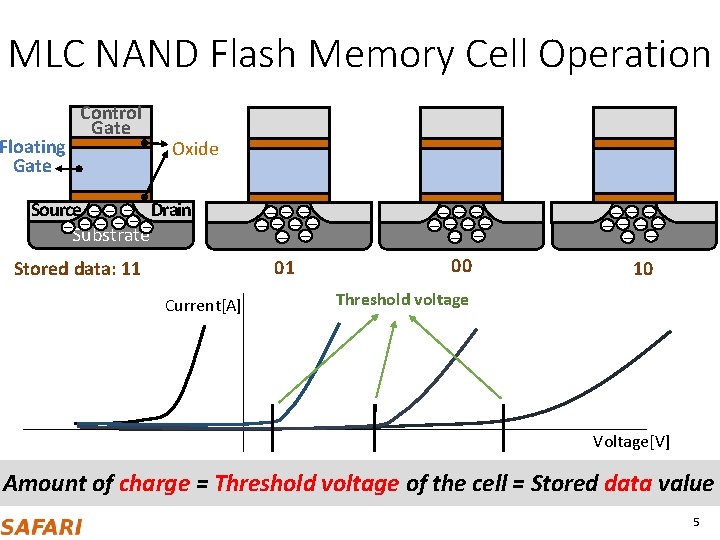
MLC NAND Flash Memory Cell Operation Floating Gate Control Gate Oxide Source – – –– Drain – – – Substrate Stored data: 11 Current[A] –– – – – – 01 00 –– – – – – 10 Threshold voltage Voltage[V] Amount of charge = Threshold voltage of the cell = Stored data value 5
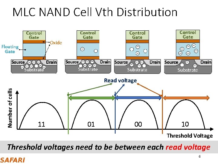
MLC NAND Cell Vth Distribution Number of cells Read voltage 11 01 00 10 Threshold Voltage Threshold voltages need to be between each read voltage 6
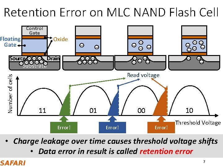
Retention Error on MLC NAND Flash Cell Floating Gate Control Gate Oxide Number of cells Source – – –– Drain – – – Substrate – – – –– – – – – – Read voltage 01 11 Error! 10 00 Error! Threshold Voltage • Charge leakage over time causes threshold voltage shifts • Data error in result is called retention error 7
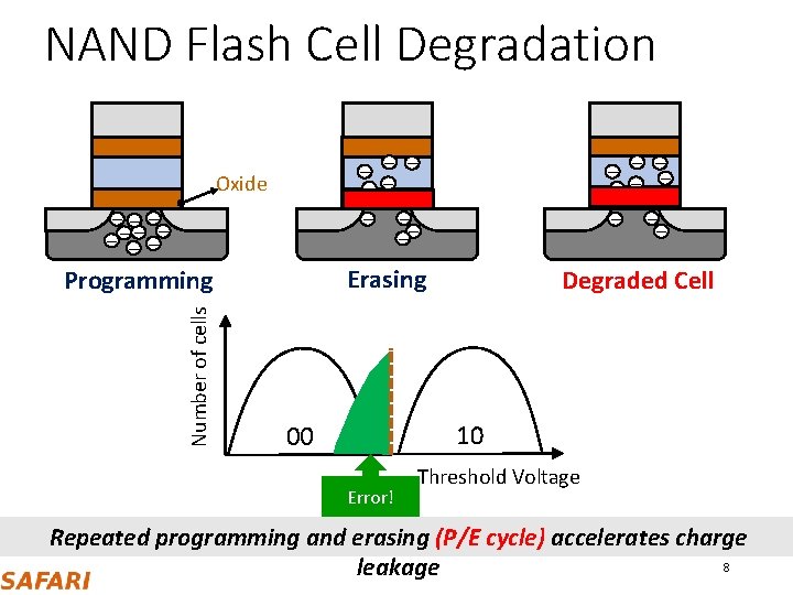
NAND Flash Cell Degradation – – – Oxide –– – – –– – Erasing Programming Number of cells – – – – – Degraded Cell 10 00 Error! Threshold Voltage Repeated programming and erasing (P/E cycle) accelerates charge 8 leakage
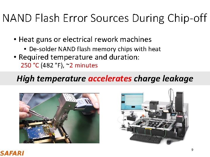
NAND Flash Error Sources During Chip-off • Heat guns or electrical rework machines • De-solder NAND flash memory chips with heat • Required temperature and duration: 250 °C (482 °F), ~2 minutes High temperature accelerates charge leakage 9
Error Correction Codes (ECC) • Flash memory controllers store ECC codewords to correct errors in data • Typical correction capability for recent chip: 40 bits correction capability per 1 KB • Errors exceeding ECC correction capability: uncorrectable errors 10
Talk Outline • Background • Basic operation of NAND flash memory • Testing Methodology and Experimental Results • Retention error • Errors introduced by heat • How to Improve Reliability of Chip-off Analysis • Read-retry operation 11
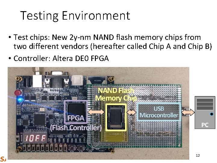
Testing Environment • Test chips: New 2 y-nm NAND flash memory chips from two different vendors (hereafter called Chip A and Chip B) • Controller: Altera DE 0 FPGA 12
Testing Methodology: Retention Error Evaluation • Repeated programming/erasing cycles (P/E cycles) • 10, 300, 1000, 2500, and 4000 cycles • Raw bit error rate (RBER) measurement at multiple retention age (=wait time after programming) • Day 0 and 1, Week 1, 2, 3 and 4 13
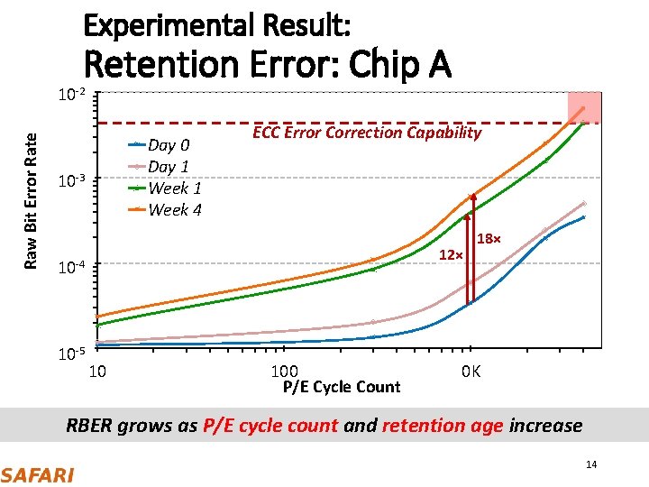
Experimental Result: Retention Error: Chip A Raw Bit Error Rate 10 -2 Day 0 Day 1 Week 4 10 -3 ECC Error Correction Capability 12× 10 -4 10 -5 10 100 P/E Cycle Count 18× 0 K RBER grows as P/E cycle count and retention age increase 14
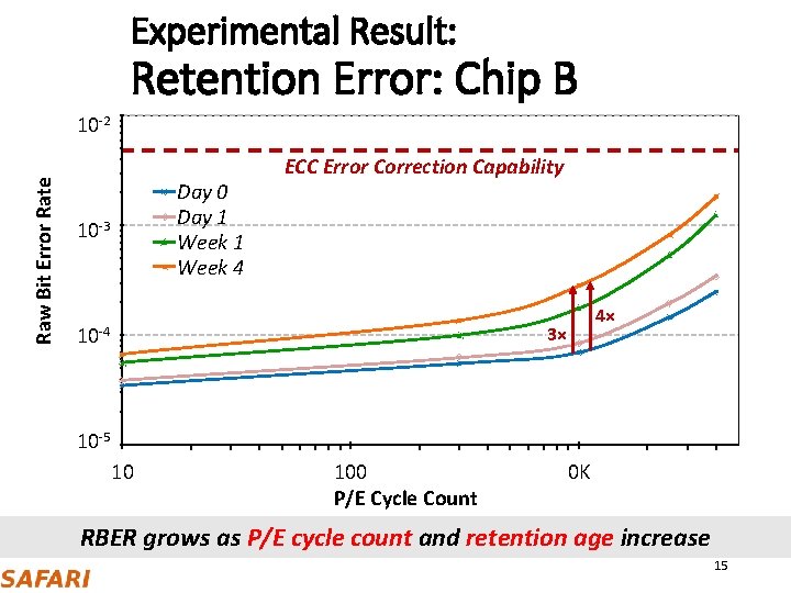
Experimental Result: Retention Error: Chip B Raw Bit Error Rate 10 -2 Day 0 Day 1 Week 4 10 -3 ECC Error Correction Capability 4× 3× 10 -4 10 -5 10 100 P/E Cycle Count 0 K RBER grows as P/E cycle count and retention age increase 15
Testing Methodology: Thermal Effect Evaluation • Baking target chips at 250 °C for 2 mins at different retention age (simulating chip-off procedures) • 1 Week • 4 Weeks • Raw bit error rate (RBER) measurement after baking 16
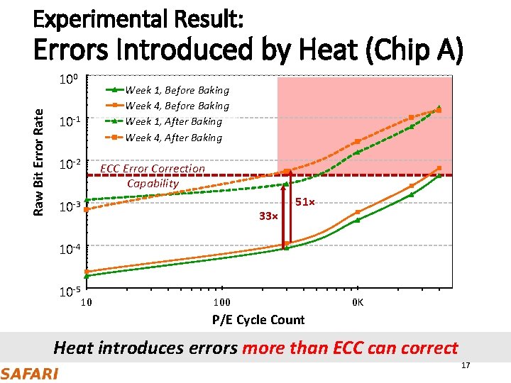
Experimental Result: Errors Introduced by Heat (Chip A) Raw Bit Error Rate 100 Week 1, Before Baking Week 4, Before Baking Week 1, After Baking Week 4, After Baking 10 -1 10 -2 ECC Error Correction Capability 10 -3 33× 51× 10 -4 10 -5 10 100 0 K P/E Cycle Count Heat introduces errors more than ECC can correct 17
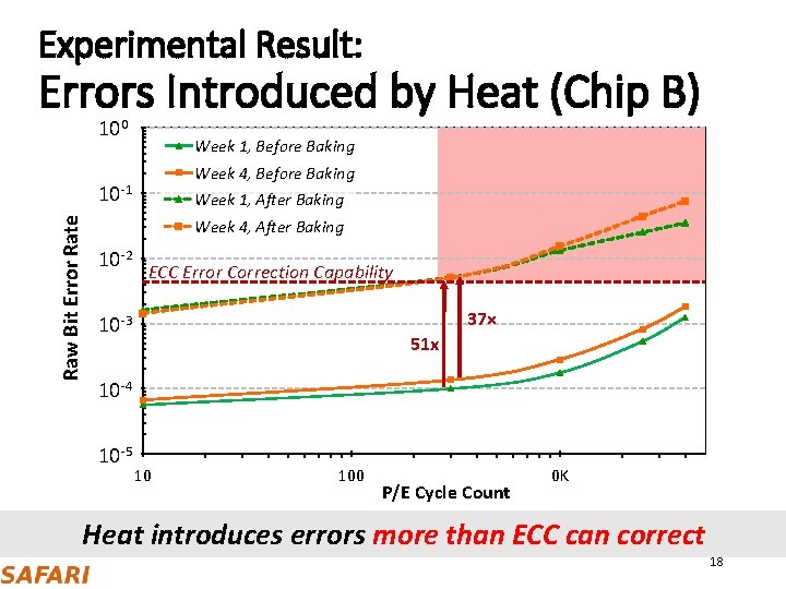
Experimental Result: Errors Introduced by Heat (Chip B) 100 Week 1, Before Baking Week 4, Before Baking Raw Bit Error Rate 10 -1 Week 1, After Baking Week 4, After Baking 10 -2 ECC Error Correction Capability 37× 10 -3 51 x 10 -4 10 -5 10 100 P/E Cycle Count 0 K Heat introduces errors more than ECC can correct 18
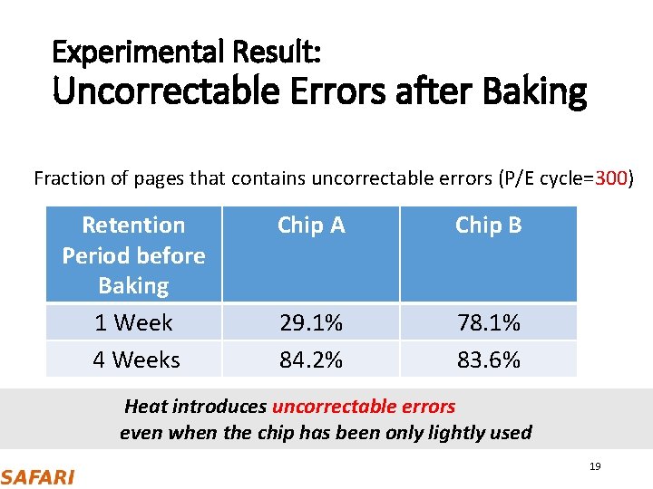
Experimental Result: Uncorrectable Errors after Baking Fraction of pages that contains uncorrectable errors (P/E cycle=300) Retention Period before Baking 1 Week 4 Weeks Chip A Chip B 29. 1% 84. 2% 78. 1% 83. 6% Heat introduces uncorrectable errors even when the chip has been only lightly used 19
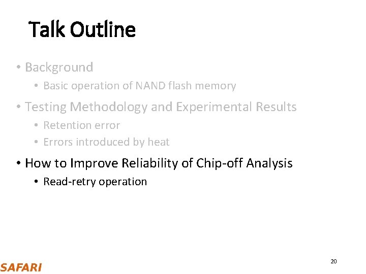
Talk Outline • Background • Basic operation of NAND flash memory • Testing Methodology and Experimental Results • Retention error • Errors introduced by heat • How to Improve Reliability of Chip-off Analysis • Read-retry operation 20
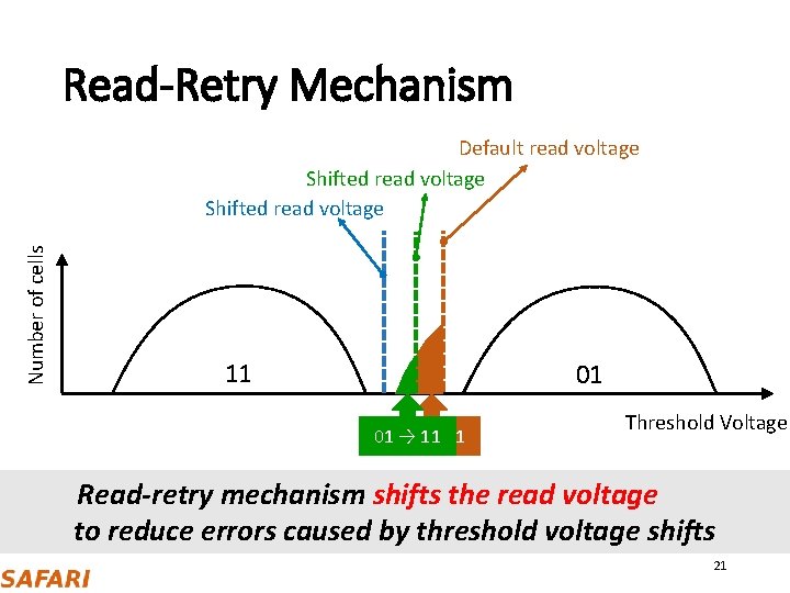
Read-Retry Mechanism Number of cells Default read voltage Shifted read voltage 11 01 01 01 → 11 Threshold Voltage Read-retry mechanism shifts the read voltage to reduce errors caused by threshold voltage shifts 21
Testing Methodology: Read-Retry Evaluation • Read-Retry command found on chip B • Implemented as a vendor specific command • Read operation with read-retry • Evaluation of 2 modes (mode A and B) 22
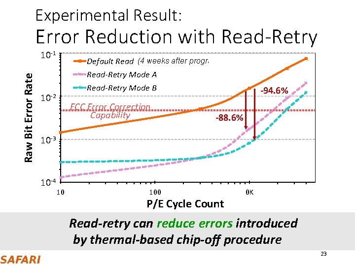
Experimental Result: Error Reduction with Read-Retry Raw Bit Error Rate 10 -1 Default Read (4 weeks after programming) Read-Retry Mode A Read-Retry Mode B 10 -2 ECC Error Correction Capability -94. 6% -88. 6% 10 -3 10 -4 10 100 P/E Cycle Count 0 K Read-retry can reduce errors introduced by thermal-based chip-off procedure 23
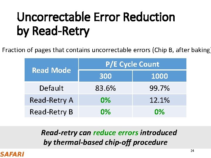
Uncorrectable Error Reduction by Read-Retry Fraction of pages that contains uncorrectable errors (Chip B, after baking) Read Mode Default Read-Retry A Read-Retry B P/E Cycle Count 300 1000 83. 6% 99. 7% 0% 12. 1% 0% 0% Read-retry can reduce errors introduced by thermal-based chip-off procedure 24
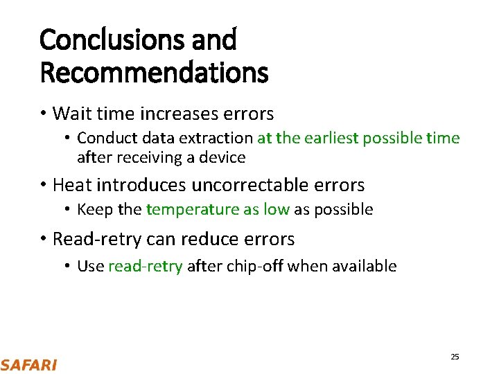
Conclusions and Recommendations • Wait time increases errors • Conduct data extraction at the earliest possible time after receiving a device • Heat introduces uncorrectable errors • Keep the temperature as low as possible • Read-retry can reduce errors • Use read-retry after chip-off when available 25

Improving the Reliability of Chip-Off Forensic Analysis of NAND Flash Memory Devices Aya Fukami, Saugata Ghose, Yixin Luo, Yu Cai, Onur Mutlu
- Slides: 26