Implementing Tilebased Chip Multiprocessors with GALS Clocking Styles
Implementing Tile-based Chip Multiprocessors with GALS Clocking Styles Zhiyi Yu, Bevan Baas VLSI Computation Lab, ECE Department University of California, Davis, USA
Outline • Introduction • Timing issues • Scalability issues • A design example
Tile-based Chip Multiprocessors and GALS Clocking Style • Chip multiprocessors – High performance due to parallel computing – Potential high energy efficiency since high performance may allow reducing clock and voltage • Tile-based architecture – Highly scalable • Globally Asynchronous Locally Synchronous – Simplified clock tree design – High energy efficiency from adaptive clock/voltage scaling for each module
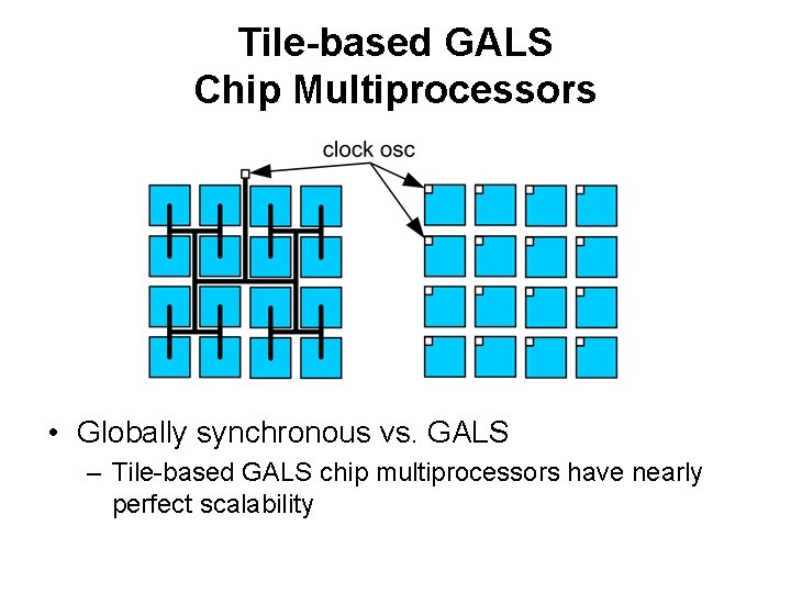
Tile-based GALS Chip Multiprocessors • Globally synchronous vs. GALS – Tile-based GALS chip multiprocessors have nearly perfect scalability
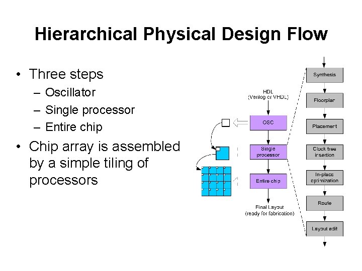
Hierarchical Physical Design Flow • Three steps – Oscillator – Single processor – Entire chip • Chip array is assembled by a simple tiling of processors
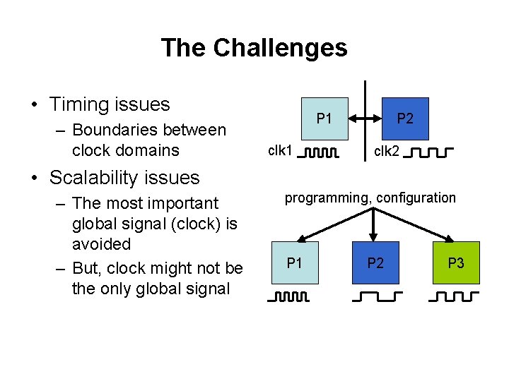
The Challenges • Timing issues – Boundaries between clock domains P 1 clk 1 P 2 clk 2 • Scalability issues – The most important global signal (clock) is avoided – But, clock might not be the only global signal programming, configuration P 1 P 2 P 3
Outline • Introduction • Timing issues • Scalability issues • A design example
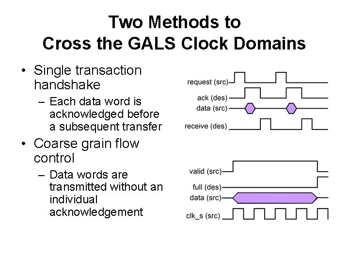
Two Methods to Cross the GALS Clock Domains • Single transaction handshake – Each data word is acknowledged before a subsequent transfer • Coarse grain flow control – Data words are transmitted without an individual acknowledgement

Overview of Timing Issues • Signal categories between processor A and B – A to B clock, synchronizing the source signals – A to B signals, data and other signals such as “valid” – B to A signals, such as “ready” or “hold” signals • Each processor contains two clock domains

Two Clock Domains within One Processor • Use dual-clock FIFO to handle the unrelated read and write clock within one processor • Multiple Flip-flops are inserted at the clock domain boundary as a configurable synchronizer
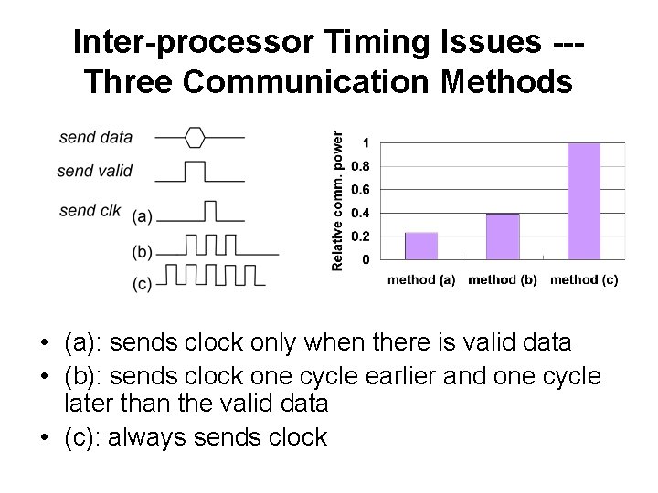
Inter-processor Timing Issues --Three Communication Methods • (a): sends clock only when there is valid data • (b): sends clock one cycle earlier and one cycle later than the valid data • (c): always sends clock
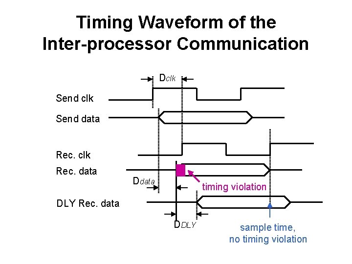
Timing Waveform of the Inter-processor Communication Dclk Send data Rec. clk Rec. data Ddata timing violation DLY Rec. data DDLY sample time, no timing violation
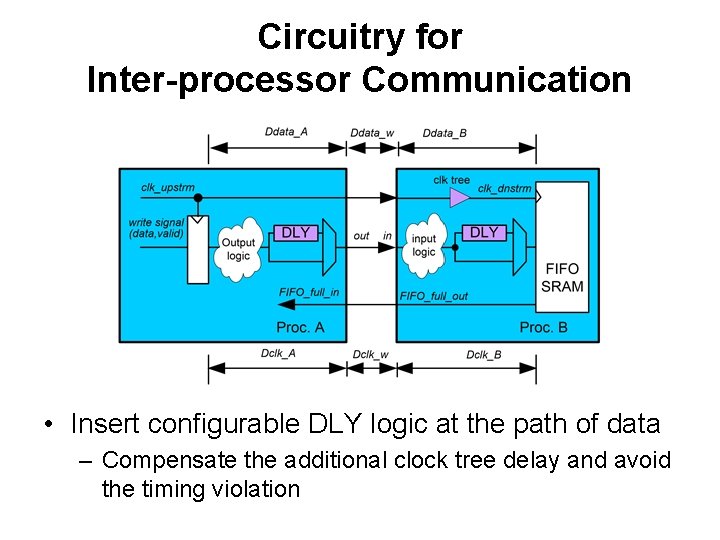
Circuitry for Inter-processor Communication • Insert configurable DLY logic at the path of data – Compensate the additional clock tree delay and avoid the timing violation

Inter-chip Communication • Inter-chip communication shares similar features with inter-processor communication • The path is longer and the timing is more complex – Output processor might need low speed clock – Destination processor can operate at full speed
Outline • Introduction • Timing issues • Scalability issues • A design example
Special Signals Besides Clock • Avoiding designing a global clock enhances scalability, but there are some other signals that must be addressed to maintain high scalability – Various global signals such as configuration and test signals – Power distribution – Processor IO pins • Key idea: avoid or isolate all global signals if possible, so multiple processors can be directly tiled without further changes
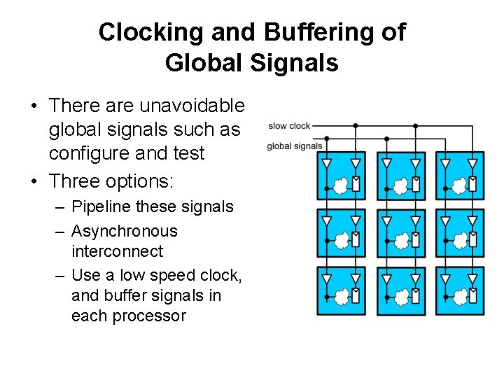
Clocking and Buffering of Global Signals • There are unavoidable global signals such as configure and test • Three options: – Pipeline these signals – Asynchronous interconnect – Use a low speed clock, and buffer signals in each processor
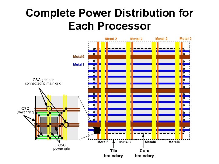
Complete Power Distribution for Each Processor
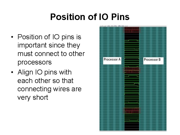
Position of IO Pins • Position of IO pins is important since they must connect to other processors • Align IO pins with each other so that connecting wires are very short
Outline • Introduction • Timing issues • Scalability issues • A design example
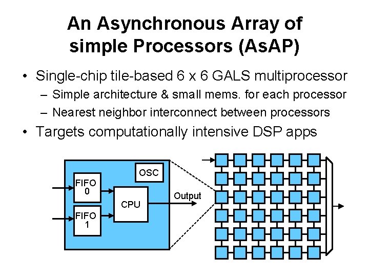
An Asynchronous Array of simple Processors (As. AP) • Single-chip tile-based 6 x 6 GALS multiprocessor – Simple architecture & small mems. for each processor – Nearest neighbor interconnect between processors • Targets computationally intensive DSP apps OSC FIFO 0 CPU FIFO 1 Output
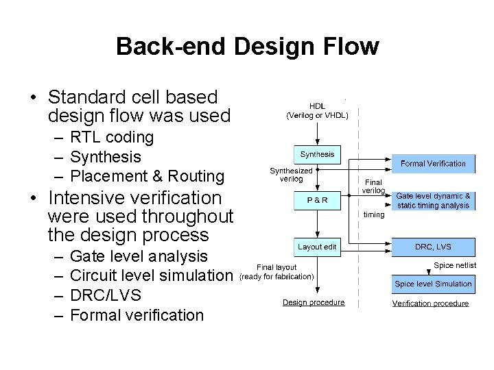
Back-end Design Flow • Standard cell based design flow was used – RTL coding – Synthesis – Placement & Routing • Intensive verification were used throughout the design process – – Gate level analysis Circuit level simulation DRC/LVS Formal verification
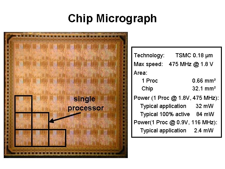
Chip Micrograph Technology: TSMC 0. 18 µm Max speed: 475 MHz @ 1. 8 V Area: 1 Proc Chip single processor 0. 66 mm² 32. 1 mm² Power (1 Proc @ 1. 8 V, 475 MHz): Typical application 32 m. W Typical 100% active 84 m. W Power(1 Proc @ 0. 9 V, 116 MHz): Typical application 2. 4 m. W
Summary • GALS tile-based chip multiprocessor is an attractive architecture – High performance, energy efficient, and highly scalable • Timing issues – Multiple clock domains in one single processor – Inter-processor communication – Inter-chip communication • Scalability issues – “Global” signals – Power distribution – IO pins

Acknowledgments • Funding – – Intel Corporation UC Micro NSF Grant No. 0430090 UCD Faculty Research Grant • Special Thanks – E. Work, D. Truong, W. Cheng, T. Jacobson, T. Mohsenin, R. Krishinamurthy, M. Anders, and S. Mathew – MOSIS – Artisan
- Slides: 25