Image sensor design with Incremental ADC in standard

- Slides: 1

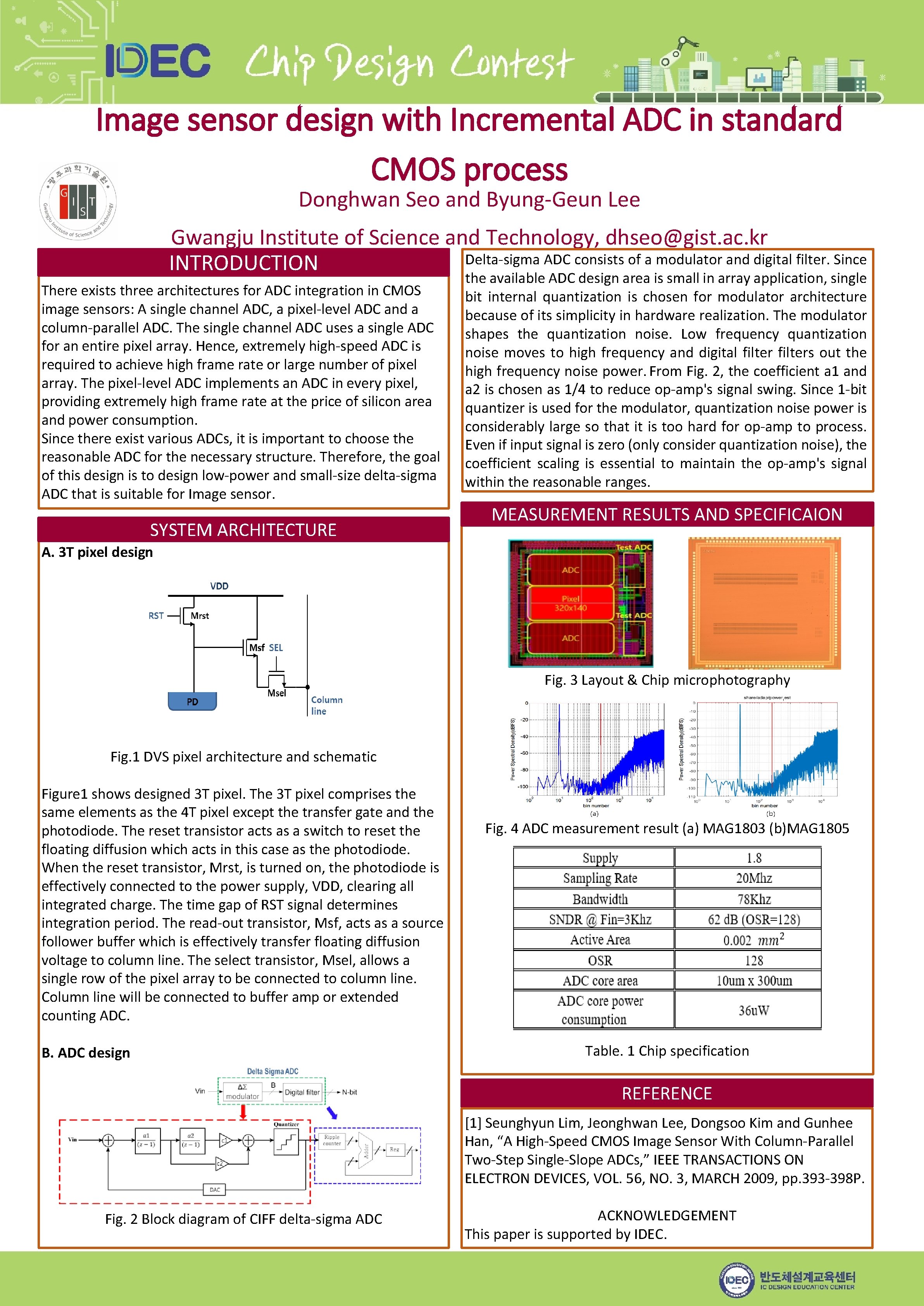
Image sensor design with Incremental ADC in standard CMOS process Donghwan Seo and Byung-Geun Lee Gwangju Institute of Science and Technology, dhseo@gist. ac. kr Delta-sigma ADC consists of a modulator and digital filter. Since INTRODUCTION There exists three architectures for ADC integration in CMOS image sensors: A single channel ADC, a pixel-level ADC and a column-parallel ADC. The single channel ADC uses a single ADC for an entire pixel array. Hence, extremely high-speed ADC is required to achieve high frame rate or large number of pixel array. The pixel-level ADC implements an ADC in every pixel, providing extremely high frame rate at the price of silicon area and power consumption. Since there exist various ADCs, it is important to choose the reasonable ADC for the necessary structure. Therefore, the goal of this design is to design low-power and small-size delta-sigma ADC that is suitable for Image sensor. SYSTEM ARCHITECTURE the available ADC design area is small in array application, single bit internal quantization is chosen for modulator architecture because of its simplicity in hardware realization. The modulator shapes the quantization noise. Low frequency quantization noise moves to high frequency and digital filters out the high frequency noise power. From Fig. 2, the coefficient a 1 and a 2 is chosen as 1/4 to reduce op-amp's signal swing. Since 1 -bit quantizer is used for the modulator, quantization noise power is considerably large so that it is too hard for op-amp to process. Even if input signal is zero (only consider quantization noise), the coefficient scaling is essential to maintain the op-amp's signal within the reasonable ranges. MEASUREMENT RESULTS AND SPECIFICAION A. 3 T pixel design Fig. 3 Layout & Chip microphotography Fig. 1 DVS pixel architecture and schematic Figure 1 shows designed 3 T pixel. The 3 T pixel comprises the same elements as the 4 T pixel except the transfer gate and the photodiode. The reset transistor acts as a switch to reset the floating diffusion which acts in this case as the photodiode. When the reset transistor, Mrst, is turned on, the photodiode is effectively connected to the power supply, VDD, clearing all integrated charge. The time gap of RST signal determines integration period. The read-out transistor, Msf, acts as a source follower buffer which is effectively transfer floating diffusion voltage to column line. The select transistor, Msel, allows a single row of the pixel array to be connected to column line. Column line will be connected to buffer amp or extended counting ADC. B. ADC design Fig. 4 ADC measurement result (a) MAG 1803 (b)MAG 1805 Table. 1 Chip specification REFERENCE [1] Seunghyun Lim, Jeonghwan Lee, Dongsoo Kim and Gunhee Han, “A High-Speed CMOS Image Sensor With Column-Parallel Two-Step Single-Slope ADCs, ” IEEE TRANSACTIONS ON ELECTRON DEVICES, VOL. 56, NO. 3, MARCH 2009, pp. 393 -398 P. Fig. 2 Block diagram of CIFF delta-sigma ADC ACKNOWLEDGEMENT This paper is supported by IDEC.