
Image Sensor Design and Technology Development at Fraunhofer

- Slides: 27
Image Sensor Design and Technology Development at Fraunhofer IMS Dr. Sascha Weyers © Fraunhofer IMS Version 6. 1.
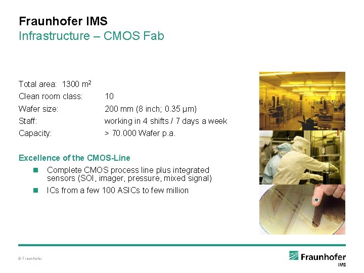
Fraunhofer IMS Infrastructure – CMOS Fab Total area: 1300 m 2 Clean room class: 10 Wafer size: 200 mm (8 inch; 0. 35 µm) Staff: working in 4 shifts / 7 days a week Capacity: > 70. 000 Wafer p. a. Excellence of the CMOS-Line n Complete CMOS process line plus integrated sensors (SOI, imager, pressure, mixed signal) n ICs from a few 100 ASICs to few million © Fraunhofer
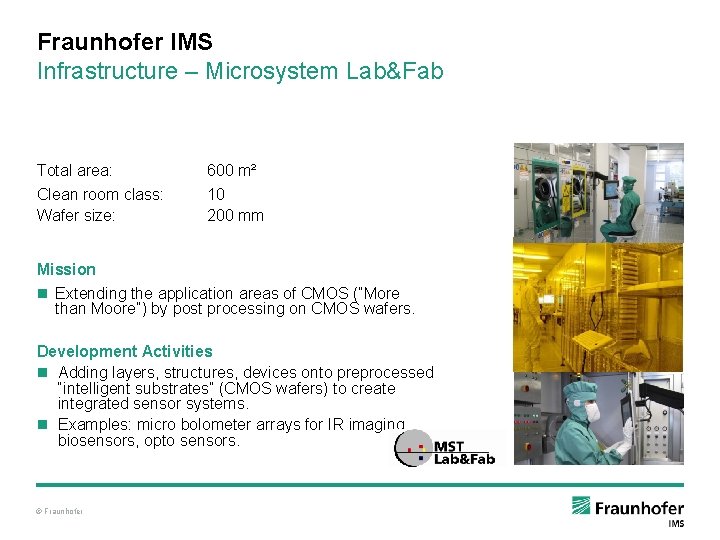
Fraunhofer IMS Infrastructure – Microsystem Lab&Fab Total area: Clean room class: Wafer size: 600 m² 10 200 mm Mission n Extending the application areas of CMOS (“More than Moore”) by post processing on CMOS wafers. Development Activities n Adding layers, structures, devices onto preprocessed “intelligent substrates” (CMOS wafers) to create integrated sensor systems. n Examples: micro bolometer arrays for IR imaging, biosensors, opto sensors. © Fraunhofer
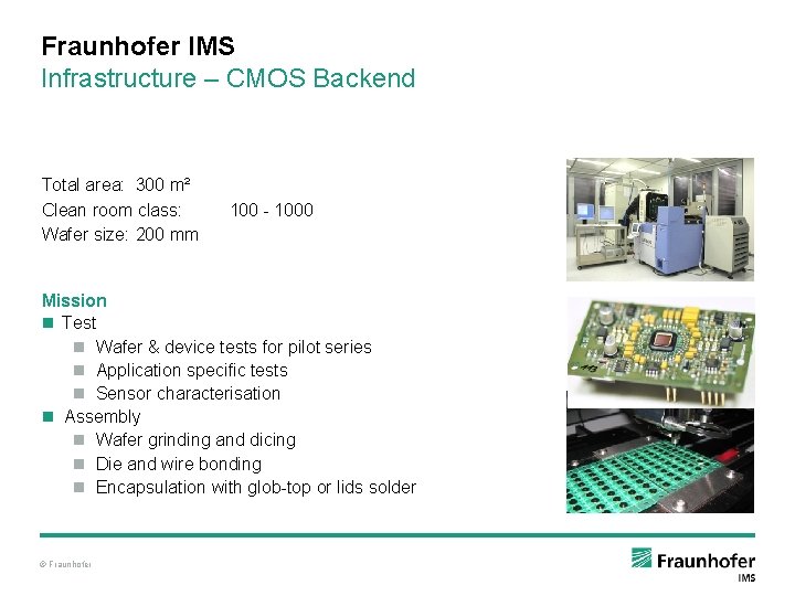
Fraunhofer IMS Infrastructure – CMOS Backend Total area: 300 m² Clean room class: Wafer size: 200 mm 100 - 1000 Mission n Test n Wafer & device tests for pilot series n Application specific tests n Sensor characterisation n Assembly n Wafer grinding and dicing n Die and wire bonding n Encapsulation with glob-top or lids solder © Fraunhofer
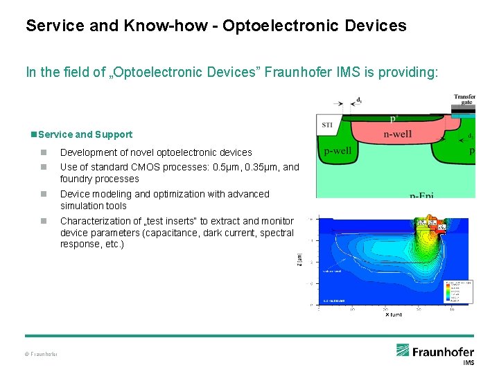
Service and Know-how - Optoelectronic Devices In the field of „Optoelectronic Devices” Fraunhofer IMS is providing: n. Service and Support n Development of novel optoelectronic devices n Use of standard CMOS processes: 0. 5µm, 0. 35µm, and foundry processes n Device modeling and optimization with advanced simulation tools n Characterization of „test inserts“ to extract and monitor device parameters (capacitance, dark current, spectral response, etc. ) © Fraunhofer
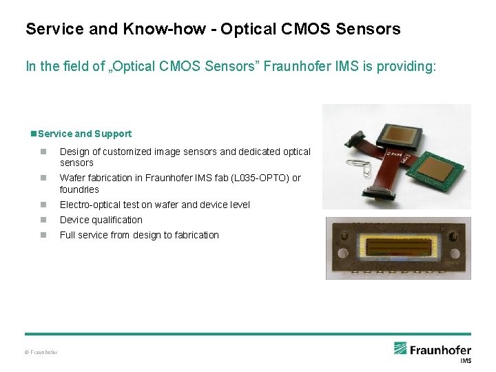
Service and Know-how - Optical CMOS Sensors In the field of „Optical CMOS Sensors” Fraunhofer IMS is providing: n. Service and Support n Design of customized image sensors and dedicated optical sensors n Wafer fabrication in Fraunhofer IMS fab (L 035 -OPTO) or foundries n Electro-optical test on wafer and device level n Device qualification n Full service from design to fabrication © Fraunhofer
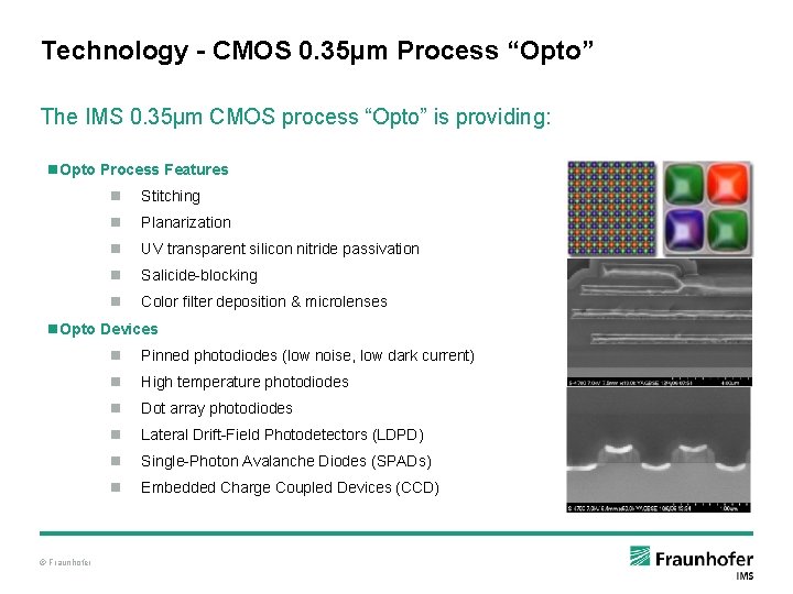
Technology - CMOS 0. 35µm Process “Opto” The IMS 0. 35µm CMOS process “Opto” is providing: n. Opto Process Features n Stitching n Planarization n UV transparent silicon nitride passivation n Salicide-blocking n Color filter deposition & microlenses n. Opto Devices © Fraunhofer n Pinned photodiodes (low noise, low dark current) n High temperature photodiodes n Dot array photodiodes n Lateral Drift-Field Photodetectors (LDPD) n Single-Photon Avalanche Diodes (SPADs) n Embedded Charge Coupled Devices (CCD)
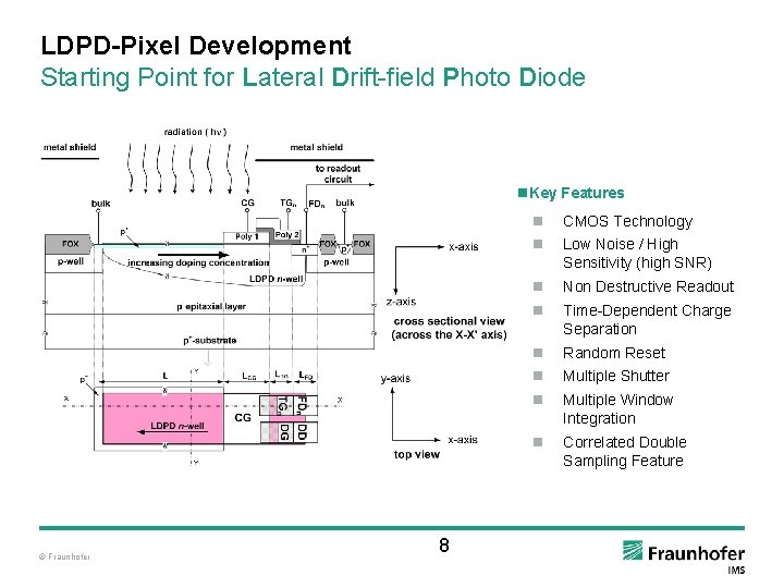
LDPD-Pixel Development Starting Point for Lateral Drift-field Photo Diode n. Key Features © Fraunhofer 8 n CMOS Technology n Low Noise / High Sensitivity (high SNR) n Non Destructive Readout n Time-Dependent Charge Separation n Random Reset n Multiple Shutter n Multiple Window Integration n Correlated Double Sampling Feature
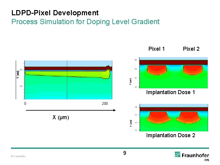
LDPD-Pixel Development Process Simulation for Doping Level Gradient Pixel 1 Pixel 2 Implantation Dose 1 0 200 X (µm) Implantation Dose 2 © Fraunhofer 9
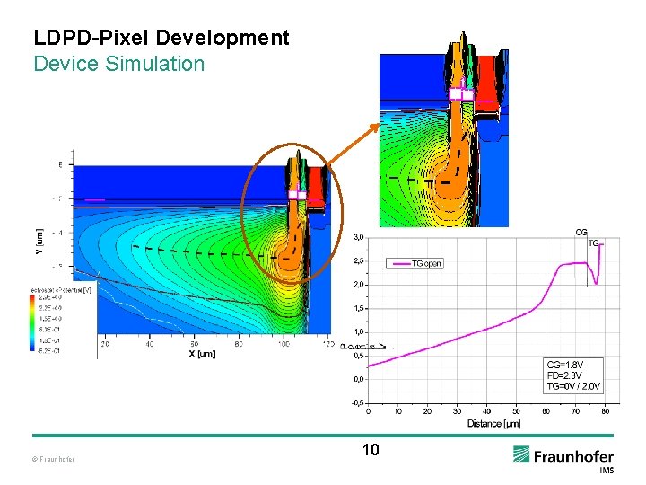
LDPD-Pixel Development Device Simulation © Fraunhofer 10
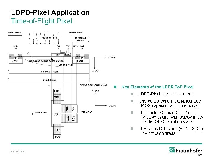
LDPD-Pixel Application Time-of-Flight Pixel n © Fraunhofer Key Elements of the LDPD To. F-Pixel n LDPD-Pixel as basic element n Charge Collection (CG)-Electrode: MOS-capacitor with gate oxide n 4 Transfer Gates (TX 1… 4): MOS-capacitor with oxide-nitrideoxide (ONO) isolation stack n 4 Floating Diffusions (FD 1… 3, DD): n+-diffusion areas
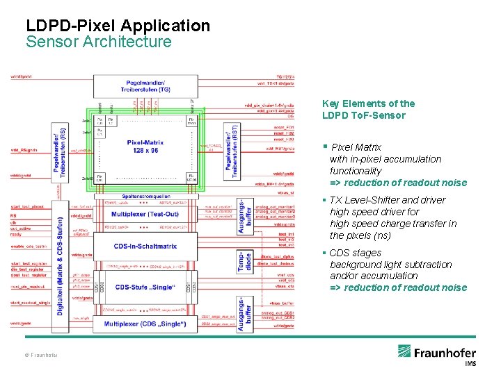
LDPD-Pixel Application Sensor Architecture Key Elements of the LDPD To. F-Sensor § Pixel Matrix with in-pixel accumulation functionality => reduction of readout noise § TX Level-Shifter and driver high speed driver for high speed charge transfer in the pixels (ns) § CDS stages background light subtraction and/or accumulation => reduction of readout noise © Fraunhofer
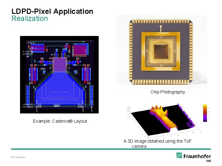
LDPD-Pixel Application Realization pixel driver 128 x 96 pixel matrix Chip Photography CDS stages Example: Cadence® Layout A 3 D image obtained using the To. F camera © Fraunhofer
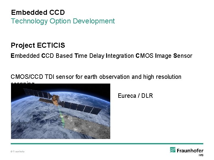
Embedded CCD Technology Option Development Project ECTICIS Embedded CCD Based Time Delay Integration CMOS Image Sensor CMOS/CCD TDI sensor for earth observation and high resolution scanning Eureca / DLR © Fraunhofer
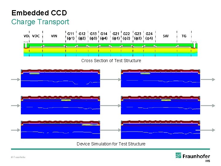
Embedded CCD Charge Transport Cross Section of Test Structure Device Simulation for Test Structure © Fraunhofer
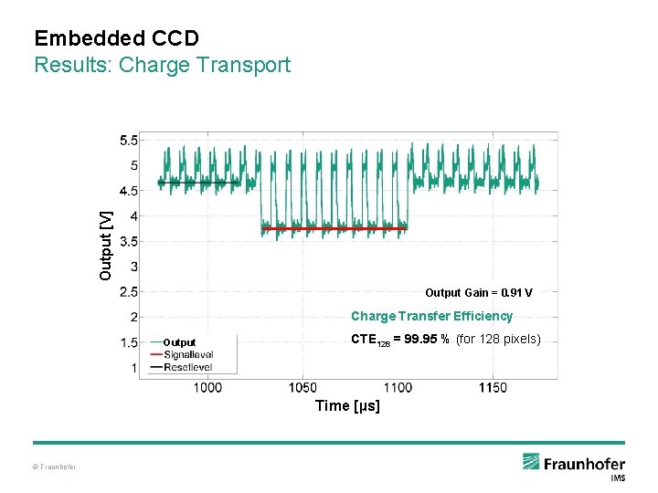
Output [V] Embedded CCD Results: Charge Transport Output Gain = 0. 91 V Charge Transfer Efficiency Output CTE 128 = 99. 95 % (for 128 pixels) Time [µs] © Fraunhofer
CMOS-SPAD Development EU Seventh Framework Programme (FP 7, 2007 -2013) Grant agreement n° 257646. © Fraunhofer
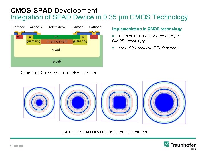
CMOS-SPAD Development Integration of SPAD Device in 0. 35 µm CMOS Technology Implementation in CMOS technology § Extension of the standard 0. 35 µm CMOS technology § Layout for primitive SPAD device Schematic Cross Section of SPAD Device Layout of SPAD Devices for different Diameters © Fraunhofer
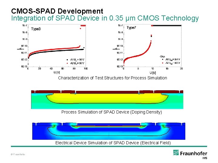
CMOS-SPAD Development Integration of SPAD Device in 0. 35 µm CMOS Technology Characterization of Test Structures for Process Simulation of SPAD Device (Doping Density) Electrical Device Simulation of SPAD Device (Electrical Field) © Fraunhofer
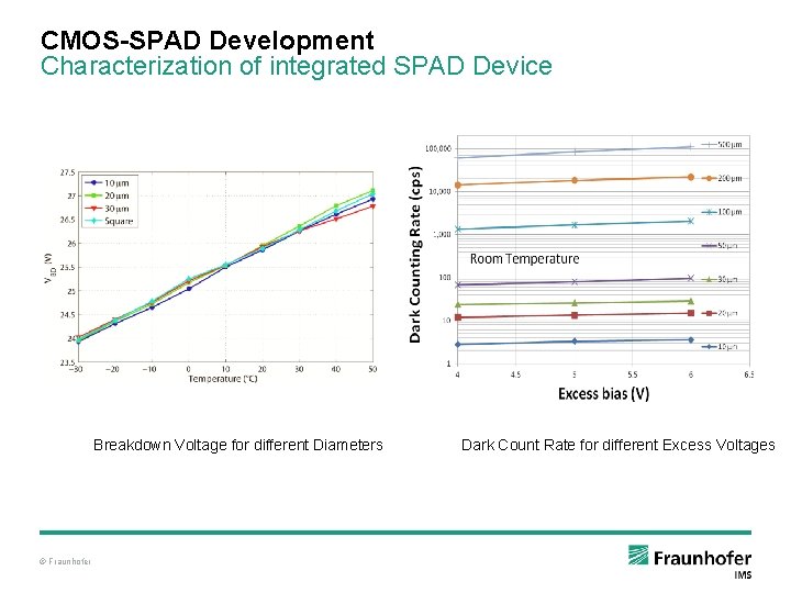
CMOS-SPAD Development Characterization of integrated SPAD Device Breakdown Voltage for different Diameters © Fraunhofer Dark Count Rate for different Excess Voltages
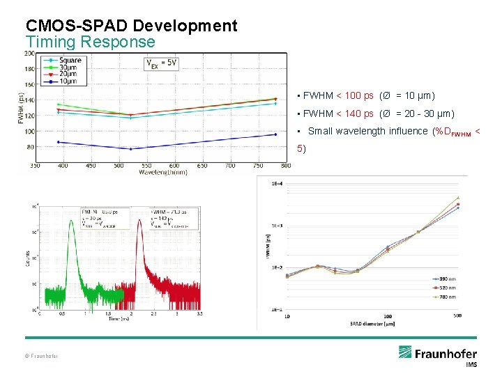
CMOS-SPAD Development Timing Response • FWHM < 100 ps (Ø = 10 µm) • FWHM < 140 ps (Ø = 20 - 30 µm) • Small wavelength influence (%DFWHM < 5) © Fraunhofer
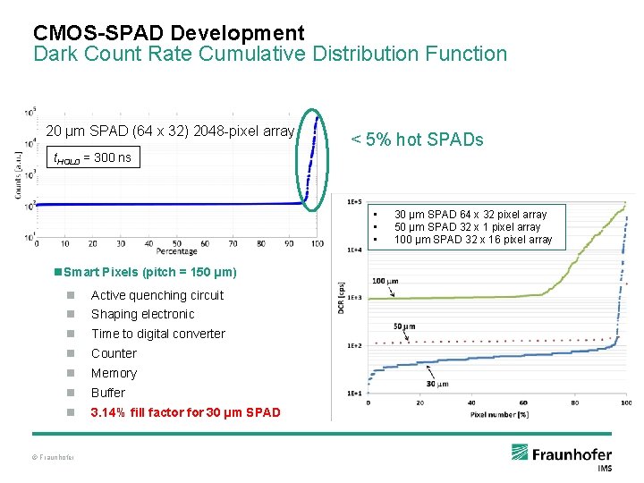
CMOS-SPAD Development Dark Count Rate Cumulative Distribution Function 20 µm SPAD (64 x 32) 2048 -pixel array < 5% hot SPADs t. HOLD = 300 ns • • • n. Smart Pixels (pitch = 150 µm) n Active quenching circuit n Shaping electronic n Time to digital converter n Counter n Memory n Buffer n 3. 14% fill factor for 30 µm SPAD © Fraunhofer 30 µm SPAD 64 x 32 pixel array 50 µm SPAD 32 x 1 pixel array 100 µm SPAD 32 x 16 pixel array
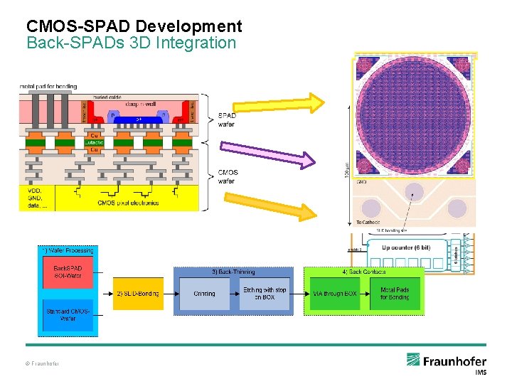
CMOS-SPAD Development Back-SPADs 3 D Integration © Fraunhofer
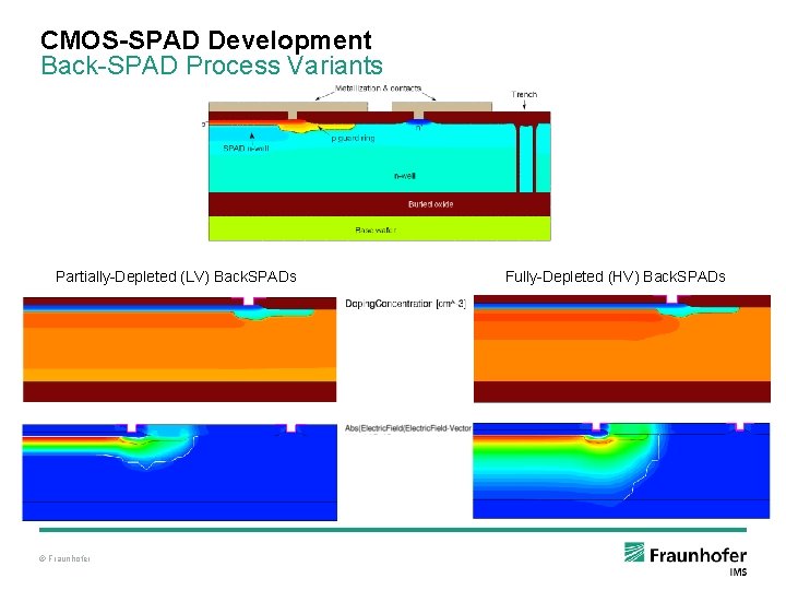
CMOS-SPAD Development Back-SPAD Process Variants Partially-Depleted (LV) Back. SPADs © Fraunhofer Fully-Depleted (HV) Back. SPADs
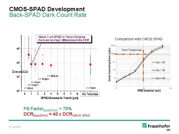
CMOS-SPAD Development Back-SPAD Dark Count Rate Comparison with CMOS SPAD Fill Factor. Back. SPAD > 70% DCRBack. SPAD ≈ 40 x DCRCMOS SPAD © Fraunhofer
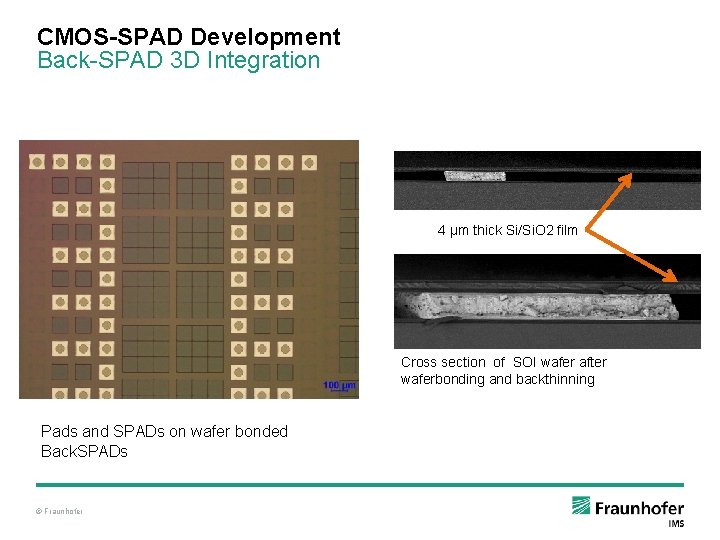
CMOS-SPAD Development Back-SPAD 3 D Integration 4 µm thick Si/Si. O 2 film Cross section of SOI wafer after waferbonding and backthinning Pads and SPADs on wafer bonded Back. SPADs © Fraunhofer
Image Sensor Design and Technology Development at Fraunhofer IMS Thank you for your Attention © Fraunhofer