
IEEE Central NC EDSMTTSSC Society Friday Nov 5
- Slides: 49
IEEE Central NC EDS/MTT/SSC Society Friday, Nov. 5 th, 2010 The Nanoscale MOSFET: Physics and Limits Mark Lundstrom Electrical and Computer Engineering and Network for Computational Nanotechnology Birck Nanotechnology Center Purdue University, West Lafayette, Indiana USA 1
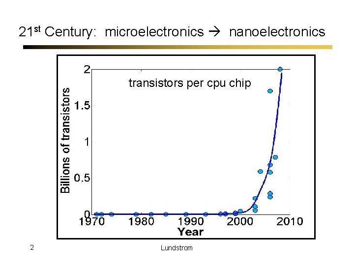
21 st Century: microelectronics nanoelectronics transistors per cpu chip 2 Lundstrom
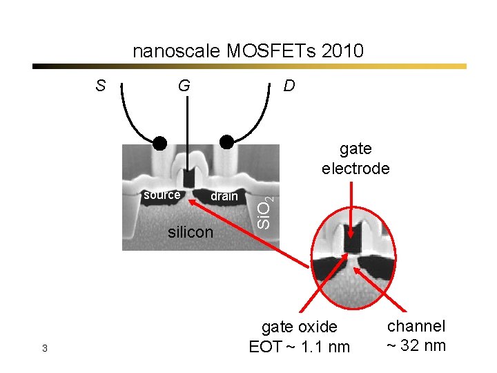
nanoscale MOSFETs 2010 S G D source drain silicon 3 Si. O 2 gate electrode gate oxide EOT ~ 1. 1 nm channel ~ 32 nm
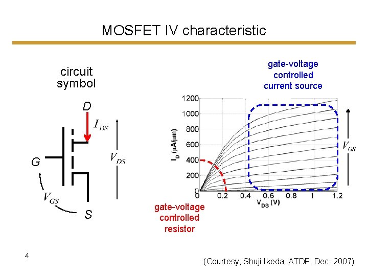
MOSFET IV characteristic gate-voltage controlled current source circuit symbol D G S 4 gate-voltage controlled resistor (Courtesy, Shuji Ikeda, ATDF, Dec. 2007)
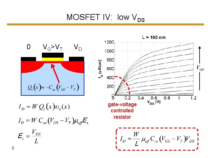
MOSFET IV: low VDS 0 VG>VT VD gate-voltage controlled resistor 5
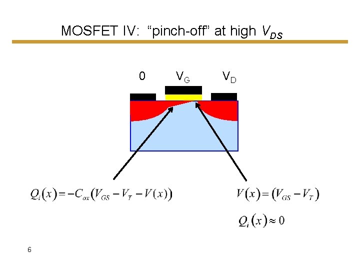
MOSFET IV: “pinch-off” at high VDS 0 6 VG VD
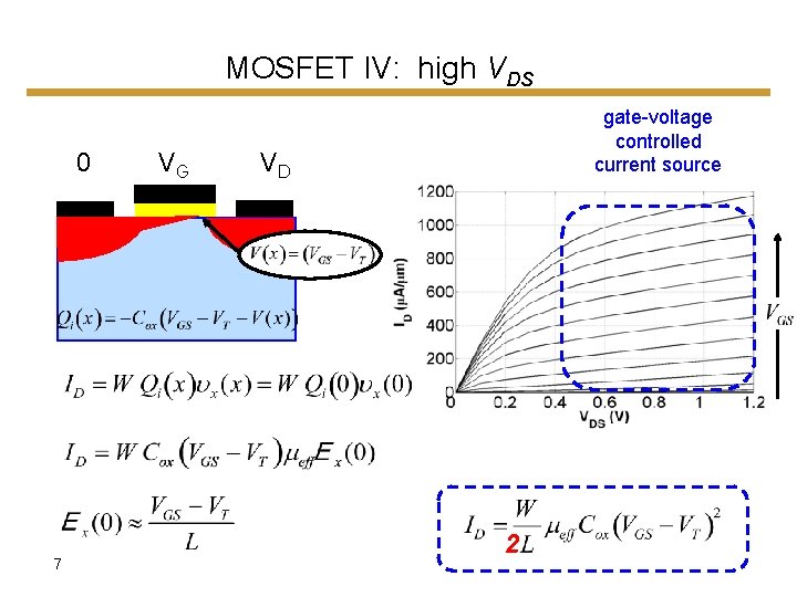
MOSFET IV: high VDS 0 7 VG gate-voltage controlled current source VD 2
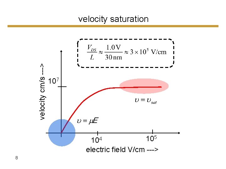
velocity cm/s ---> velocity saturation 107 105 104 electric field V/cm ---> 8
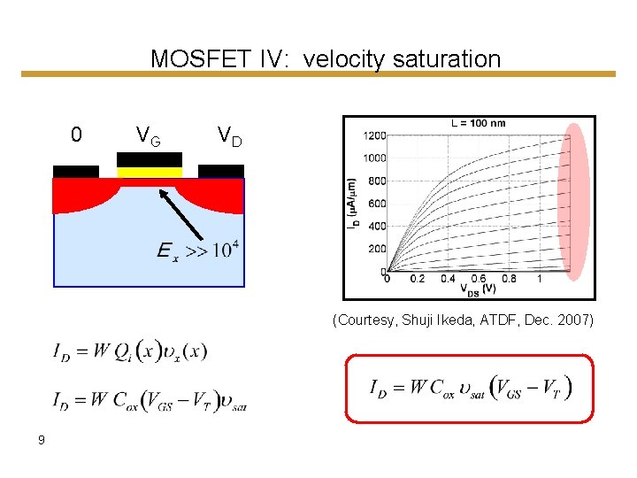
MOSFET IV: velocity saturation 0 VG VD (Courtesy, Shuji Ikeda, ATDF, Dec. 2007) 9
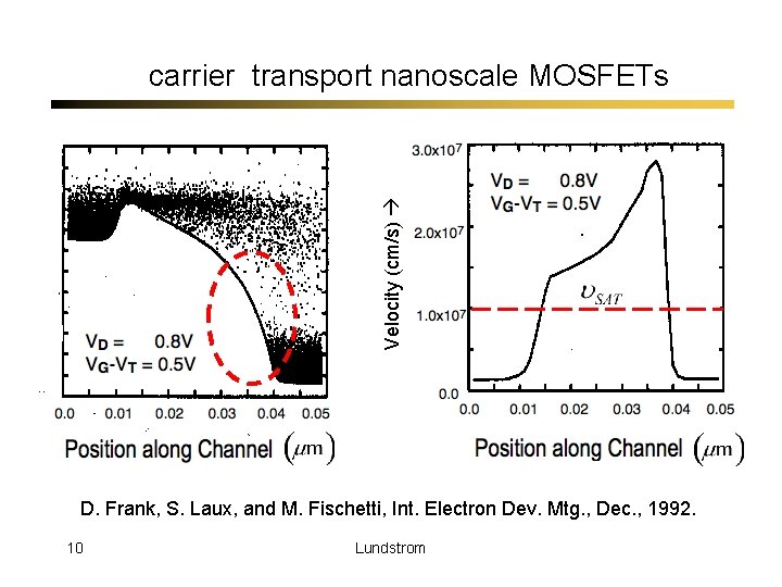
Velocity (cm/s) carrier transport nanoscale MOSFETs D. Frank, S. Laux, and M. Fischetti, Int. Electron Dev. Mtg. , Dec. , 1992. 10 Lundstrom
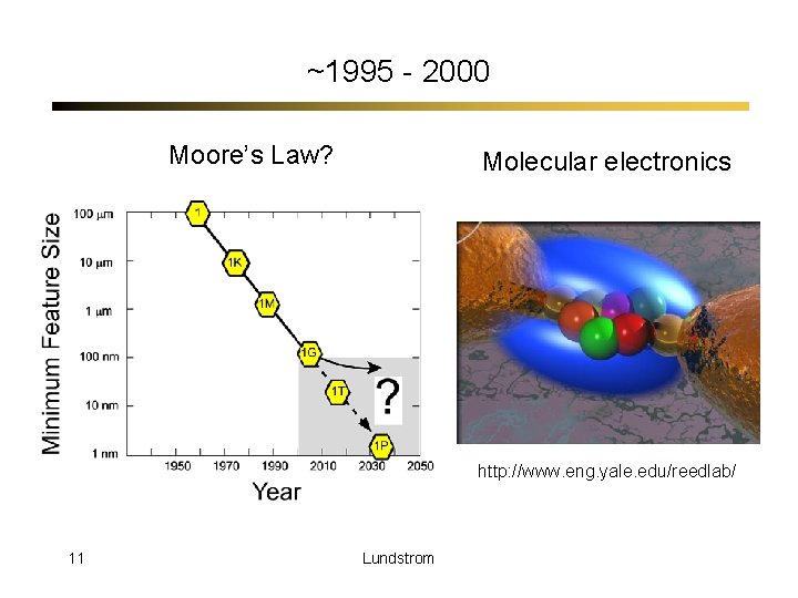
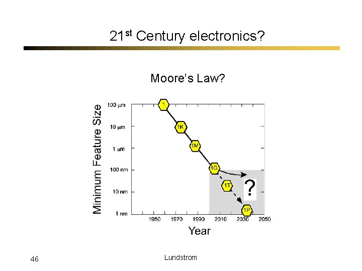
~1995 - 2000 Moore’s Law? Molecular electronics http: //www. eng. yale. edu/reedlab/ 11 Lundstrom
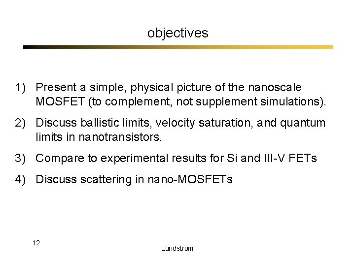
objectives 1) Present a simple, physical picture of the nanoscale MOSFET (to complement, not supplement simulations). 2) Discuss ballistic limits, velocity saturation, and quantum limits in nanotransistors. 3) Compare to experimental results for Si and III-V FETs 4) Discuss scattering in nano-MOSFETs 12 Lundstrom
outline 1) Introduction 2) The nano-MOSFET 3) The ballistic MOSFET 4) Scattering in nano-MOSFETs 5) Summary Lundstrom 13
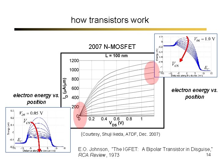
how transistors work 2007 N-MOSFET electron energy vs. position (Courtesy, Shuji Ikeda, ATDF, Dec. 2007) E. O. Johnson, “The IGFET: A Bipolar Transistor in Disguise, ” 14 RCA Review, 1973
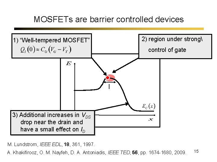
MOSFETs are barrier controlled devices 1) “Well-tempered MOSFET” 2) region under strong control of gate 3) Additional increases in VDS drop near the drain and have a small effect on ID M. Lundstrom, IEEE EDL, 18, 361, 1997. A. Khakifirooz, O. M. Nayfeh, D. A. Antoniadis, IEEE TED, 56, pp. 1674 -1680, 2009. 15
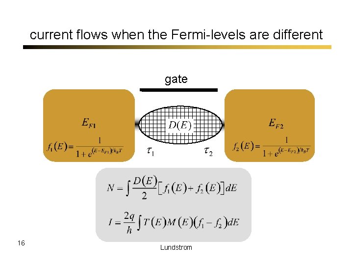
current flows when the Fermi-levels are different gate 16 Lundstrom
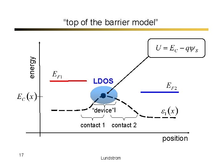
energy “top of the barrier model” LDOS “device” contact 1 contact 2 position 17 Lundstrom
outline 1) Introduction 2) The nano-MOSFET 3) The ballistic MOSFET 4) Scattering in nano-MOSFETs 5) Summary Lundstrom 18
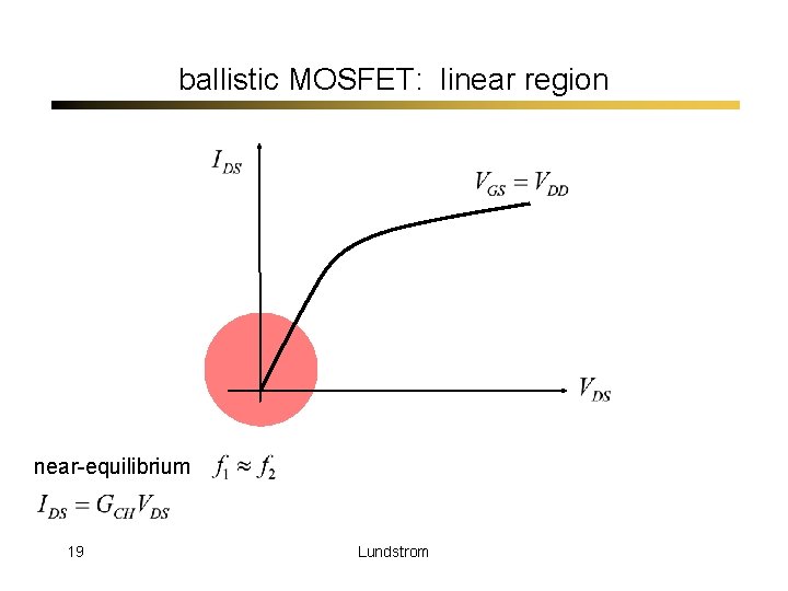
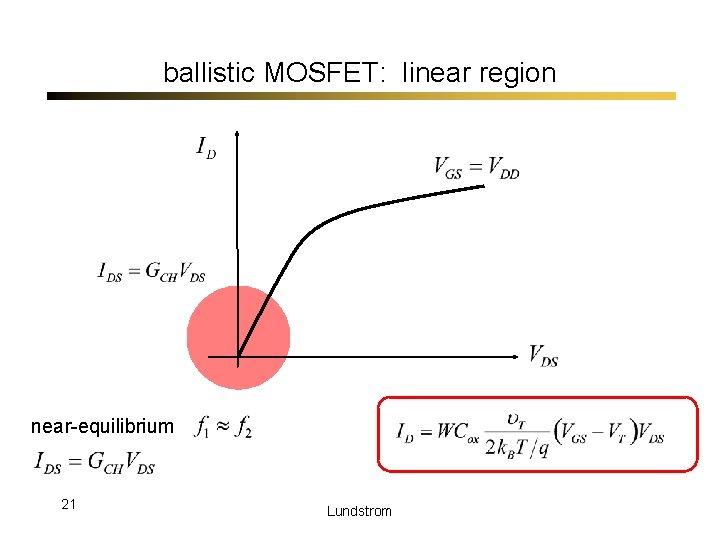
ballistic MOSFET: linear region near-equilibrium 19 Lundstrom
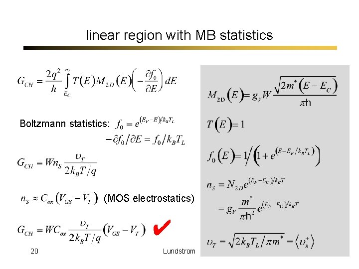
linear region with MB statistics Boltzmann statistics: (MOS electrostatics) ✔ 20 Lundstrom
ballistic MOSFET: linear region near-equilibrium 21 Lundstrom
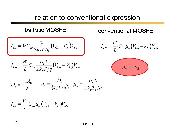
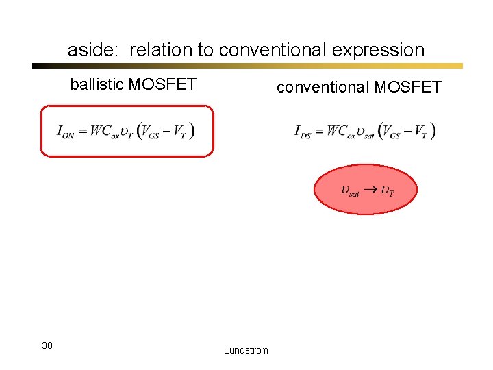
relation to conventional expression ballistic MOSFET 22 conventional MOSFET Lundstrom
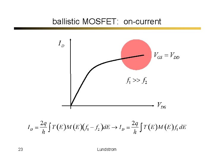
ballistic MOSFET: on-current 23 Lundstrom
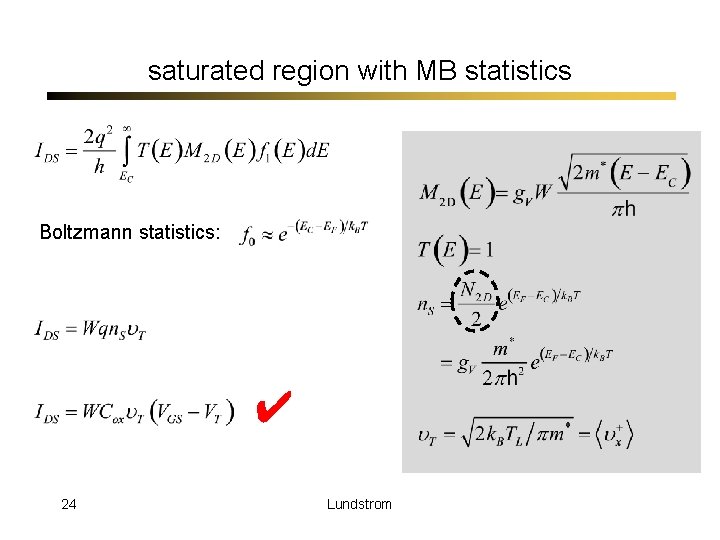
saturated region with MB statistics Boltzmann statistics: ✔ 24 Lundstrom
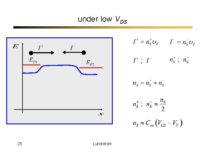
under low VDS 25 Lundstrom
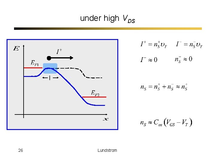
under high VDS 26 Lundstrom
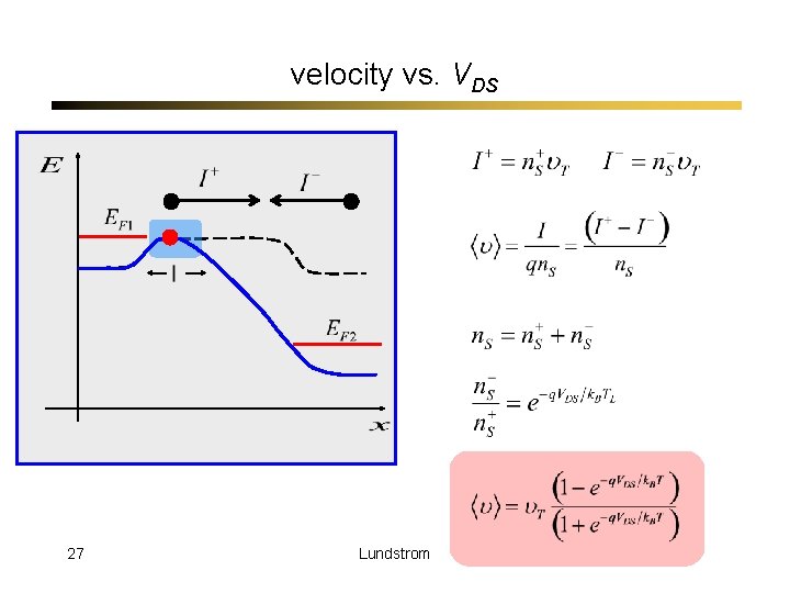
velocity vs. VDS 27 Lundstrom
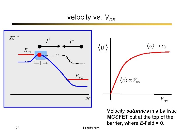
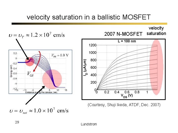
velocity vs. VDS Velocity saturates in a ballistic MOSFET but at the top of the barrier, where E-field = 0. 28 Lundstrom
velocity saturation in a ballistic MOSFET velocity 2007 N-MOSFET saturation (Courtesy, Shuji Ikeda, ATDF, Dec. 2007) 29 Lundstrom
aside: relation to conventional expression ballistic MOSFET 30 conventional MOSFET Lundstrom
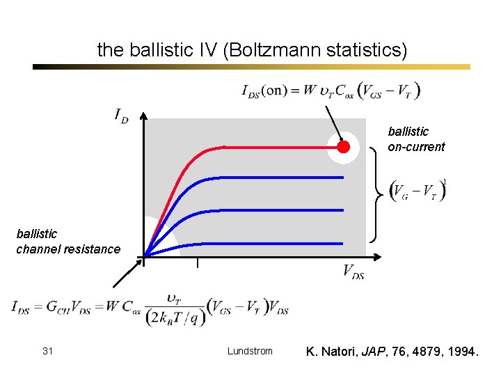
the ballistic IV (Boltzmann statistics) ballistic on-current ballistic channel resistance 31 Lundstrom K. Natori, JAP, 76, 4879, 1994.
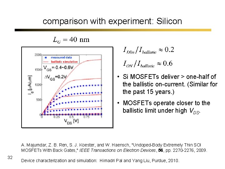
comparison with experiment: Silicon • Si MOSFETs deliver > one-half of the ballistic on-current. (Similar for the past 15 years. ) • MOSFETs operate closer to the ballistic limit under high VDS. A. Majumdar, Z. B. Ren, S. J. Koester, and W. Haensch, "Undoped-Body Extremely Thin SOI MOSFETs With Back Gates, " IEEE Transactions on Electron Devices, 56, pp. 2270 -2276, 2009. 32 Device characterization and simulation: Himadri Pal and Yang Liu, Purdue, 2010.
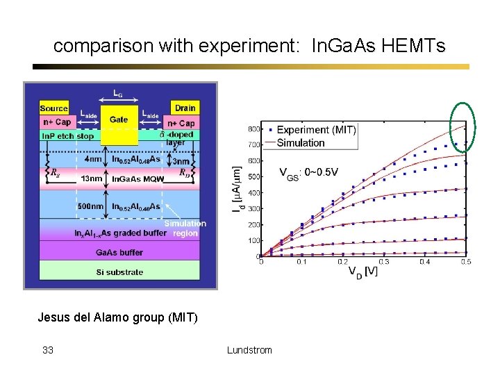
comparison with experiment: In. Ga. As HEMTs Jesus del Alamo group (MIT) 33 Lundstrom
outline 1) Introduction 2) The nano-MOSFET 3) The ballistic MOSFET 4) Scattering in nano-MOSFETs 5) Summary Lundstrom 34
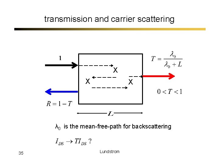
transmission and carrier scattering X X X λ 0 is the mean-free-path for backscattering 35 Lundstrom
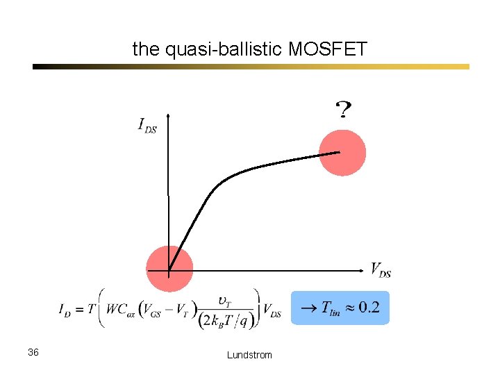
the quasi-ballistic MOSFET 36 Lundstrom
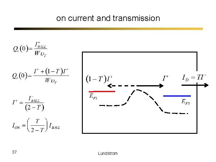
on current and transmission 37 Lundstrom
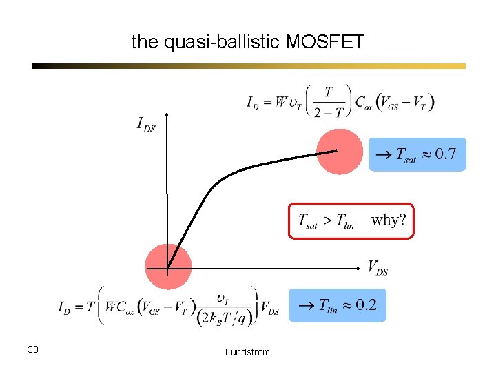
the quasi-ballistic MOSFET 38 Lundstrom
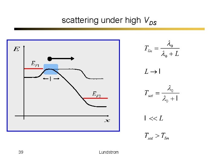
scattering under high VDS 39 Lundstrom
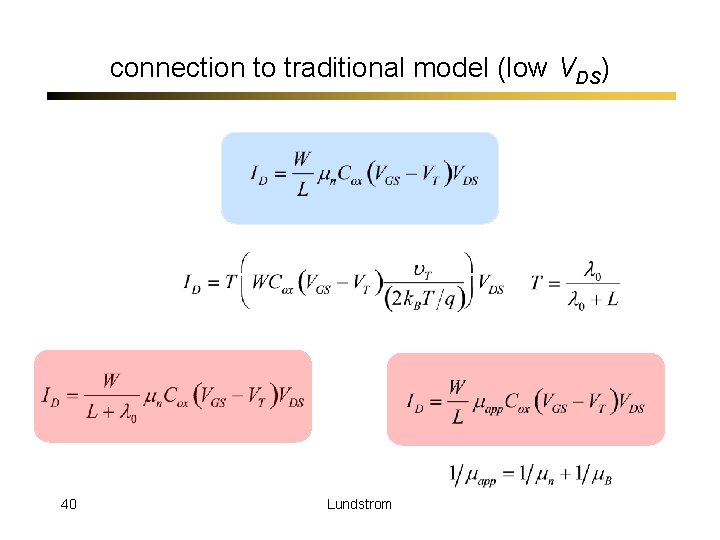
connection to traditional model (low VDS) 40 Lundstrom
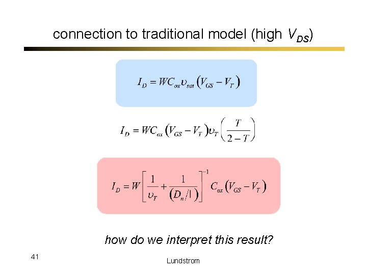
connection to traditional model (high VDS) how do we interpret this result? 41 Lundstrom
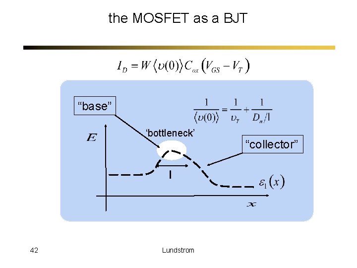
the MOSFET as a BJT “base” ‘bottleneck’ 42 Lundstrom “collector”
outline 1) Introduction 2) The nano-MOSFET 3) The ballistic MOSFET 4) Scattering in nano-MOSFETs 5) Summary Lundstrom 43
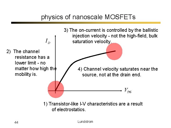
physics of nanoscale MOSFETs 3) The on-current is controlled by the ballistic injection velocity - not the high-field, bulk saturation velocity. 2) The channel resistance has a lower limit - no matter how high the mobility is. 4) Channel velocity saturates near the source, not at the drain end. 1) Transistor-like I-V characteristics are a result of electrostatics. 44 Lundstrom
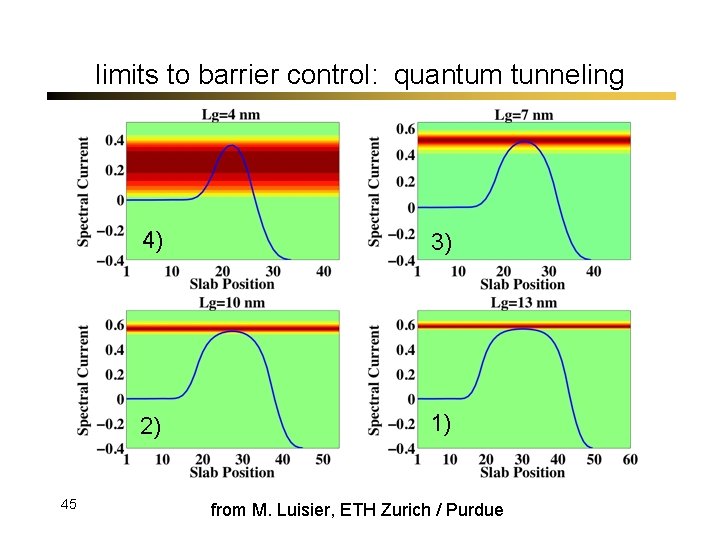
limits to barrier control: quantum tunneling 45 4) 3) 2) 1) from M. Luisier, ETH Zurich / Purdue
21 st Century electronics? Moore’s Law? 46 Lundstrom
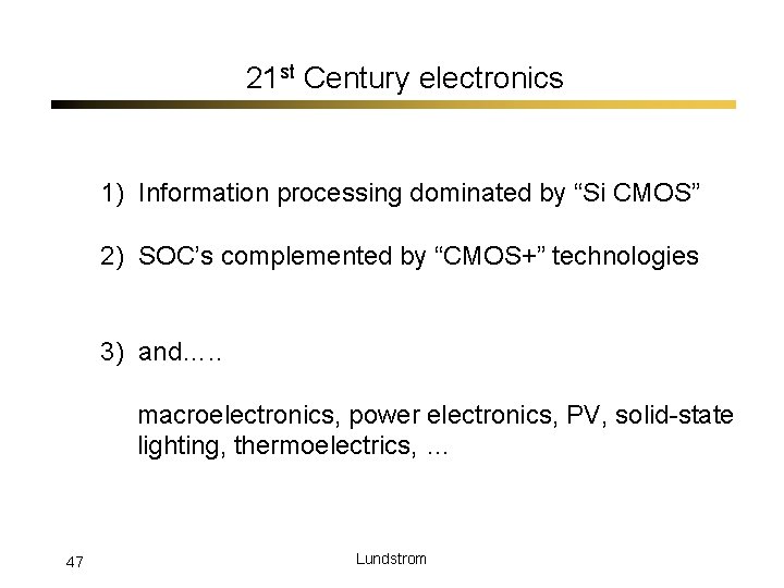
21 st Century electronics 1) Information processing dominated by “Si CMOS” 2) SOC’s complemented by “CMOS+” technologies 3) and…. . macroelectronics, power electronics, PV, solid-state lighting, thermoelectrics, … 47 Lundstrom
for more information 1) “Physics of Nanoscale MOSFETs, ” a series of eight lectures on the subject presented at the 2008 NCN@Purdue Summer School by Mark Lundstrom, 2008. http: //nanohub. org/resources/5306 2) “Electronic Transport in Semiconductors, ” Lectures 1 -7, by Mark Lundstrom, 2009. http: //nanohub. org/resources/7281 48 Lundstrom
questions 1) Introduction 2) The nano-MOSFET 3) The ballistic MOSFET 4) Scattering in nano-MOSFETs 5) Summary Lundstrom 49