IEE 5011 Autumn 2013 Memory Systems Duty Cycle
![Basic GDDR 5 (4/4) [1] Kuang-Yu, Li NCTU IEE 5011 Memory Systems 2013 7 Basic GDDR 5 (4/4) [1] Kuang-Yu, Li NCTU IEE 5011 Memory Systems 2013 7](https://slidetodoc.com/presentation_image_h/7fd2c62dd9308f8b559dc40e180c207c/image-7.jpg)
![Analog and Digital Comparison [2] n Digital DCC is preferred! l Power , range Analog and Digital Comparison [2] n Digital DCC is preferred! l Power , range](https://slidetodoc.com/presentation_image_h/7fd2c62dd9308f8b559dc40e180c207c/image-17.jpg)
![All-Digital DCC(ADDCC) [3] n Wide-range, high resolution n Combined with DLL l Low jitter All-Digital DCC(ADDCC) [3] n Wide-range, high resolution n Combined with DLL l Low jitter](https://slidetodoc.com/presentation_image_h/7fd2c62dd9308f8b559dc40e180c207c/image-18.jpg)
![DCC in GDDR 5 n Wide-range, fast-lock, offset tolerant [5] ØAnti-harmonic binary search(ABS) n DCC in GDDR 5 n Wide-range, fast-lock, offset tolerant [5] ØAnti-harmonic binary search(ABS) n](https://slidetodoc.com/presentation_image_h/7fd2c62dd9308f8b559dc40e180c207c/image-23.jpg)
![Reference n n n [1] Kho, R , et. al, “A 75 nm 7 Reference n n n [1] Kho, R , et. al, “A 75 nm 7](https://slidetodoc.com/presentation_image_h/7fd2c62dd9308f8b559dc40e180c207c/image-34.jpg)
- Slides: 34

IEE 5011 –Autumn 2013 Memory Systems Duty Cycle Correctors (DCC) In GDDR 5 SDRAM Kuang-Yu, Li Department of Electronics Engineering National Chiao Tung University li 50916 ku@gmail. com Kuang-Yu, Li 2013

Outline n Introduction n Basics ØDCC and GDDR 5 n Comparison ØAnalog and Digital DCC n All-Digital DCC n DCC in GDDR 5 n Conclusion Kuang-Yu, Li NCTU IEE 5011 Memory Systems 2013 2

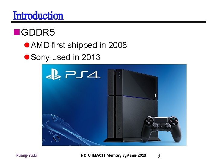
Introduction n GDDR 5 l AMD first shipped in 2008 l Sony used in 2013 Kuang-Yu, Li NCTU IEE 5011 Memory Systems 2013 3

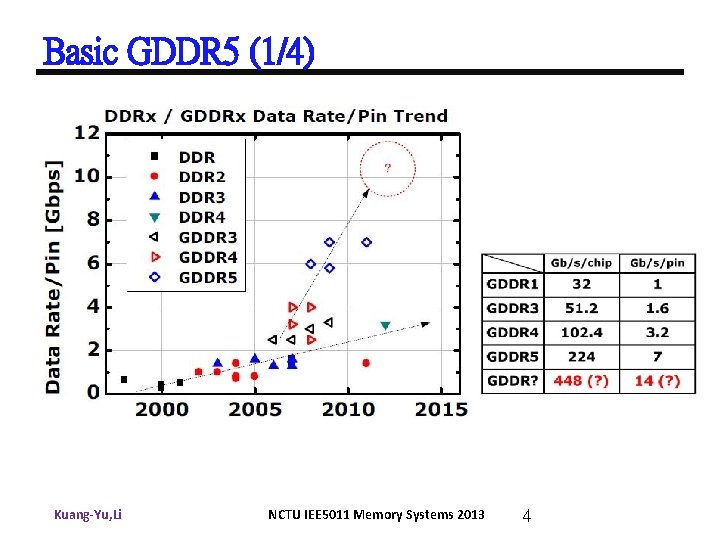
Basic GDDR 5 (1/4) Kuang-Yu, Li NCTU IEE 5011 Memory Systems 2013 4

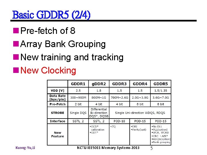
Basic GDDR 5 (2/4) n Pre-fetch of 8 n Array Bank Grouping n New training and tracking n New Clocking Kuang-Yu, Li NCTU IEE 5011 Memory Systems 2013 5

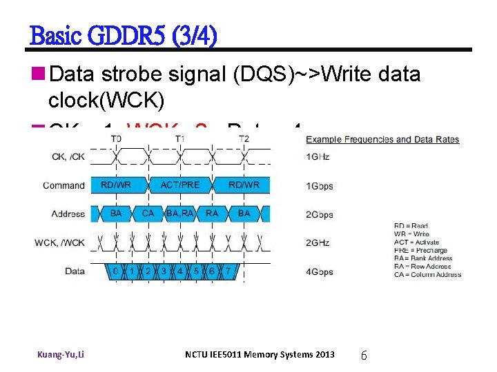
Basic GDDR 5 (3/4) n Data strobe signal (DQS)~>Write data clock(WCK) n CK x 1, WCK x 2 , Data x 4 Kuang-Yu, Li NCTU IEE 5011 Memory Systems 2013 6
![Basic GDDR 5 44 1 KuangYu Li NCTU IEE 5011 Memory Systems 2013 7 Basic GDDR 5 (4/4) [1] Kuang-Yu, Li NCTU IEE 5011 Memory Systems 2013 7](https://slidetodoc.com/presentation_image_h/7fd2c62dd9308f8b559dc40e180c207c/image-7.jpg)
Basic GDDR 5 (4/4) [1] Kuang-Yu, Li NCTU IEE 5011 Memory Systems 2013 7

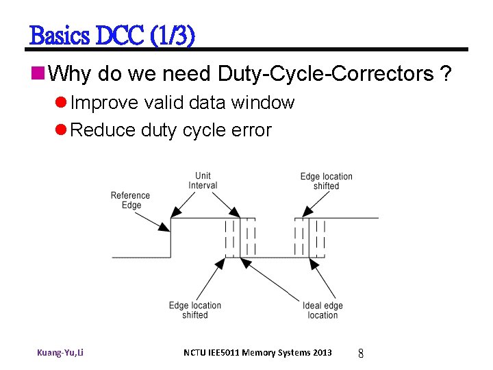
Basics DCC (1/3) n Why do we need Duty-Cycle-Correctors ? l Improve valid data window l Reduce duty cycle error Kuang-Yu, Li NCTU IEE 5011 Memory Systems 2013 8

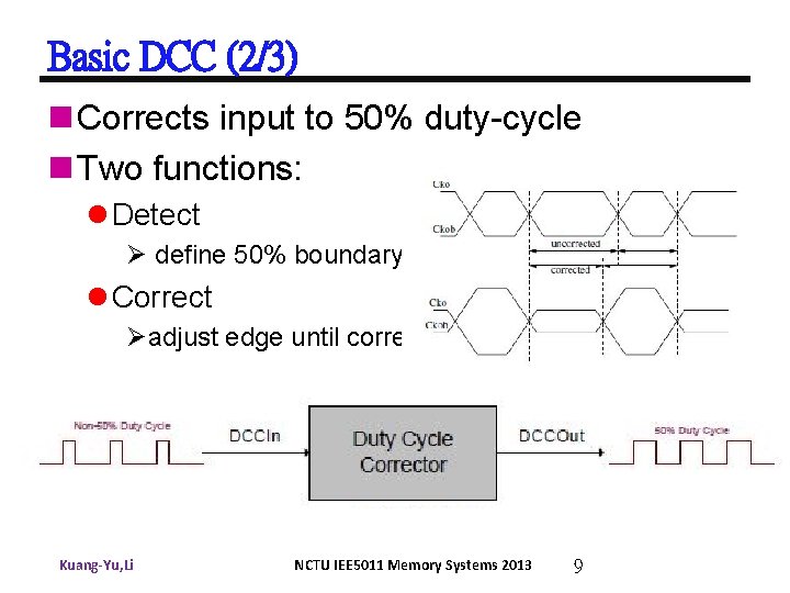
Basic DCC (2/3) n Corrects input to 50% duty-cycle n Two functions: l Detect Ø define 50% boundary l Correct Øadjust edge until correct Kuang-Yu, Li NCTU IEE 5011 Memory Systems 2013 9

Basic DCC (3/3) n Design : l Location –on/off path l Integration -embedded or not l Locking time l Operating frequency range l Offset -comes from detector l Implementation -analog or digital l Other (power, area…) Kuang-Yu, Li NCTU IEE 5011 Memory Systems 2013 10

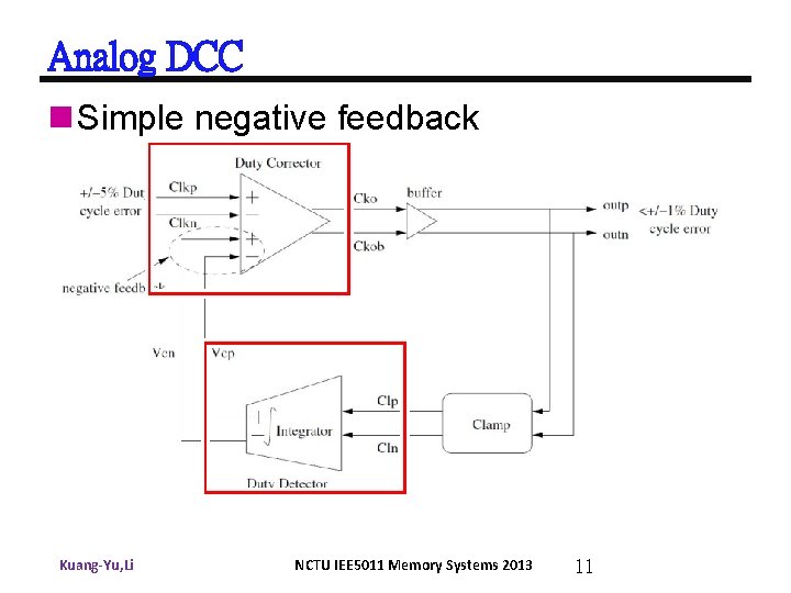
Analog DCC n Simple negative feedback Kuang-Yu, Li NCTU IEE 5011 Memory Systems 2013 11

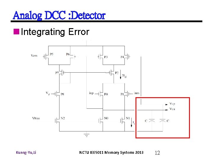
Analog DCC : Detector n Integrating Error Kuang-Yu, Li NCTU IEE 5011 Memory Systems 2013 12

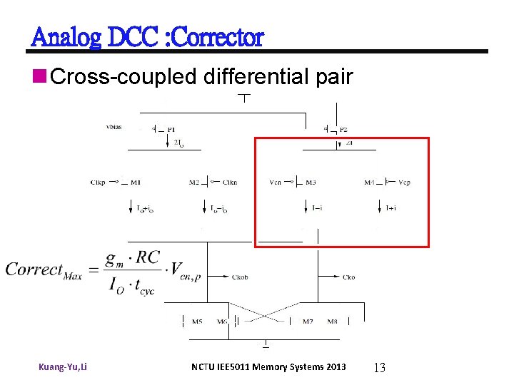
Analog DCC : Corrector n Cross-coupled differential pair Kuang-Yu, Li NCTU IEE 5011 Memory Systems 2013 13

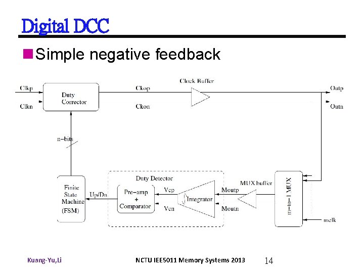
Digital DCC n Simple negative feedback Kuang-Yu, Li NCTU IEE 5011 Memory Systems 2013 14

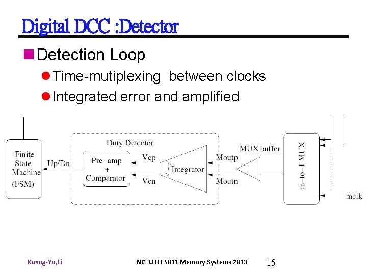
Digital DCC : Detector n Detection Loop l Time-mutiplexing between clocks l Integrated error and amplified Kuang-Yu, Li NCTU IEE 5011 Memory Systems 2013 15

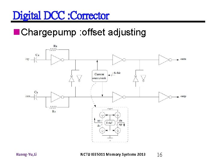
Digital DCC : Corrector n Chargepump : offset adjusting Kuang-Yu, Li NCTU IEE 5011 Memory Systems 2013 16
![Analog and Digital Comparison 2 n Digital DCC is preferred l Power range Analog and Digital Comparison [2] n Digital DCC is preferred! l Power , range](https://slidetodoc.com/presentation_image_h/7fd2c62dd9308f8b559dc40e180c207c/image-17.jpg)
Analog and Digital Comparison [2] n Digital DCC is preferred! l Power , range , function , supply, mismatch Kuang-Yu, Li Analog Digital DCC sharing X V Common mode Variation Insensitive Sensitive Correction range Narrow Wide Power Efficient X V Manual override X V NCTU IEE 5011 Memory Systems 2013 17
![AllDigital DCCADDCC 3 n Widerange high resolution n Combined with DLL l Low jitter All-Digital DCC(ADDCC) [3] n Wide-range, high resolution n Combined with DLL l Low jitter](https://slidetodoc.com/presentation_image_h/7fd2c62dd9308f8b559dc40e180c207c/image-18.jpg)
All-Digital DCC(ADDCC) [3] n Wide-range, high resolution n Combined with DLL l Low jitter and fast lock time n Open loop scheme Kuang-Yu, Li NCTU IEE 5011 Memory Systems 2013 DLL_out 18

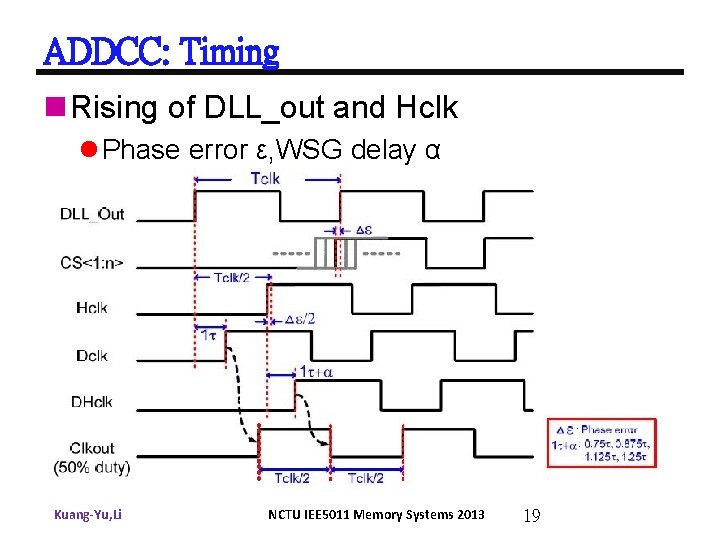
ADDCC: Timing n Rising of DLL_out and Hclk l Phase error ε, WSG delay α Kuang-Yu, Li NCTU IEE 5011 Memory Systems 2013 19

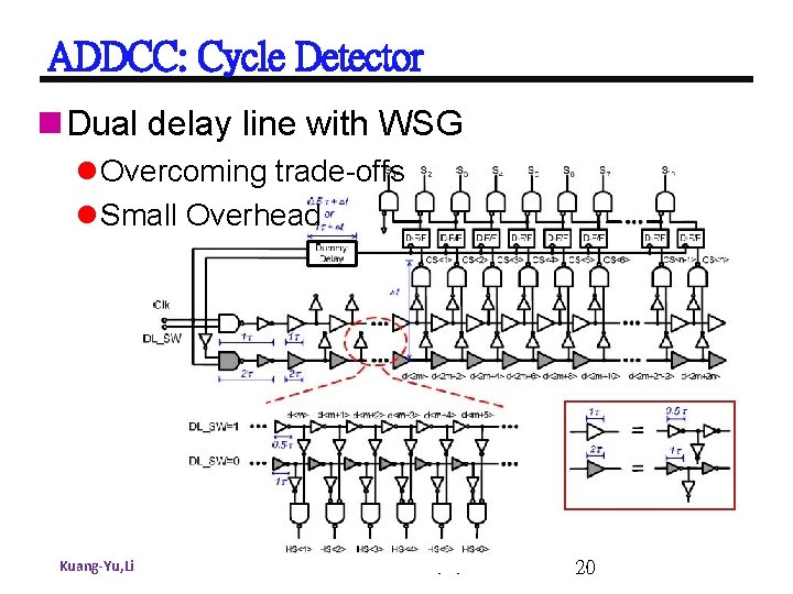
ADDCC: Cycle Detector n Dual delay line with WSG l Overcoming trade-offs l Small Overhead Kuang-Yu, Li NCTU IEE 5011 Memory Systems 2013 20

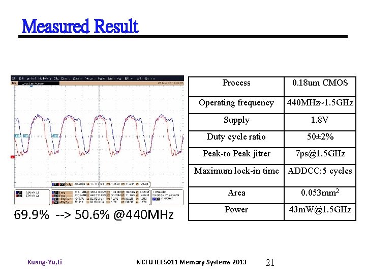
Measured Result Process 0. 18 um CMOS Operating frequency 440 MHz~1. 5 GHz Supply 1. 8 V Duty cycle ratio 50± 2% Peak-to Peak jitter 7 ps@1. 5 GHz Maximum lock-in time ADDCC: 5 cycles 69. 9% --> 50. 6% @440 MHz Kuang-Yu, Li Area 0. 053 mm 2 Power 43 m. W@1. 5 GHz NCTU IEE 5011 Memory Systems 2013 21

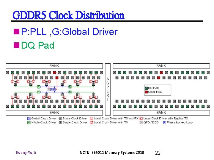
GDDR 5 Clock Distribution n P: PLL , G: Global Driver n DQ Pad Kuang-Yu, Li NCTU IEE 5011 Memory Systems 2013 22
![DCC in GDDR 5 n Widerange fastlock offset tolerant 5 ØAntiharmonic binary searchABS n DCC in GDDR 5 n Wide-range, fast-lock, offset tolerant [5] ØAnti-harmonic binary search(ABS) n](https://slidetodoc.com/presentation_image_h/7fd2c62dd9308f8b559dc40e180c207c/image-23.jpg)
DCC in GDDR 5 n Wide-range, fast-lock, offset tolerant [5] ØAnti-harmonic binary search(ABS) n CML and PLL in clock distribution Kuang-Yu, Li NCTU IEE 5011 Memory Systems 2013 23

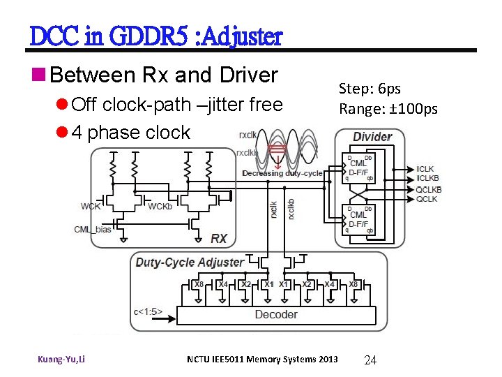
DCC in GDDR 5 : Adjuster n Between Rx and Driver l Off clock-path –jitter free l 4 phase clock Kuang-Yu, Li NCTU IEE 5011 Memory Systems 2013 Step: 6 ps Range: ± 100 ps 24

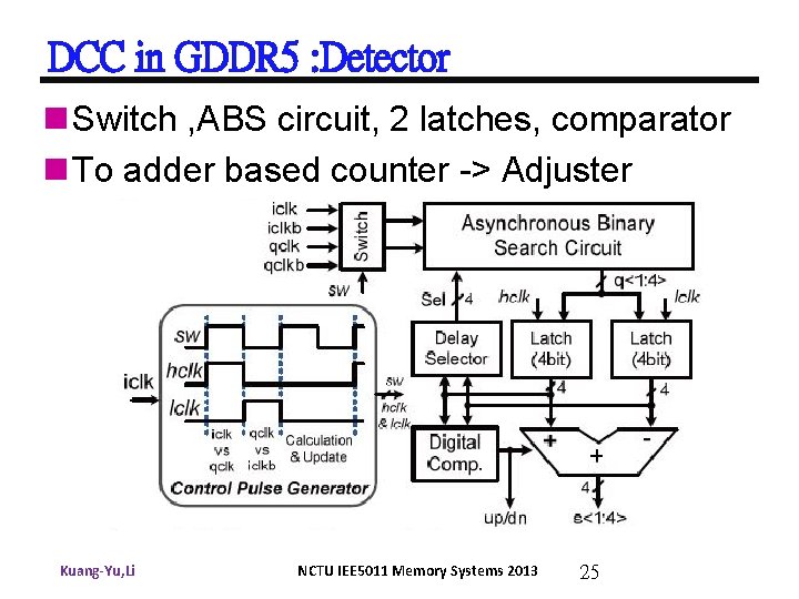
DCC in GDDR 5 : Detector n Switch , ABS circuit, 2 latches, comparator n To adder based counter -> Adjuster Kuang-Yu, Li NCTU IEE 5011 Memory Systems 2013 25

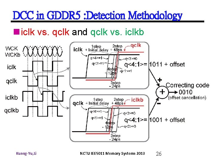
DCC in GDDR 5 : Detection Methodology n iclk vs. qclk and qclk vs. iclkb Kuang-Yu, Li NCTU IEE 5011 Memory Systems 2013 26

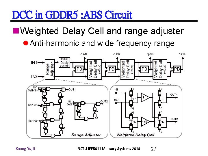
DCC in GDDR 5 : ABS Circuit n Weighted Delay Cell and range adjuster l Anti-harmonic and wide frequency range Kuang-Yu, Li NCTU IEE 5011 Memory Systems 2013 27

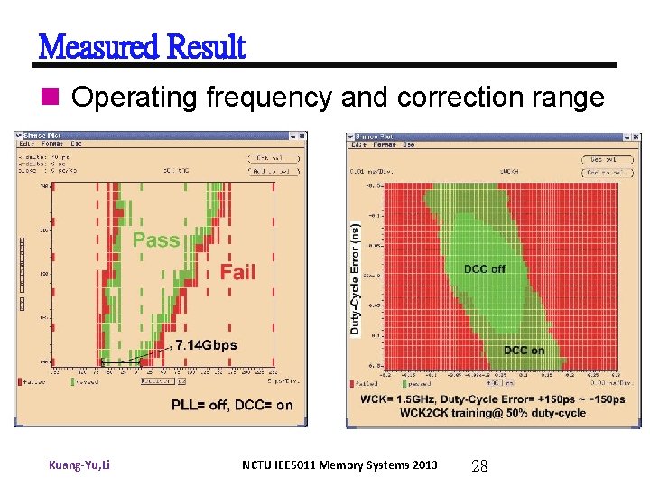
Measured Result n Operating frequency and correction range Kuang-Yu, Li NCTU IEE 5011 Memory Systems 2013 28

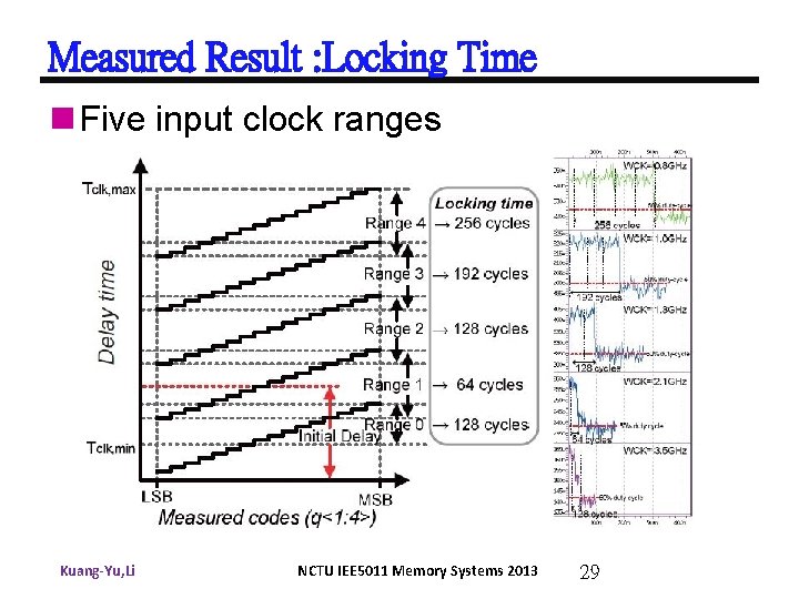
Measured Result : Locking Time n Five input clock ranges Kuang-Yu, Li NCTU IEE 5011 Memory Systems 2013 29

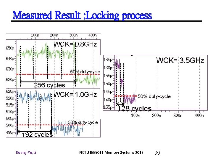
Measured Result : Locking process Kuang-Yu, Li NCTU IEE 5011 Memory Systems 2013 30

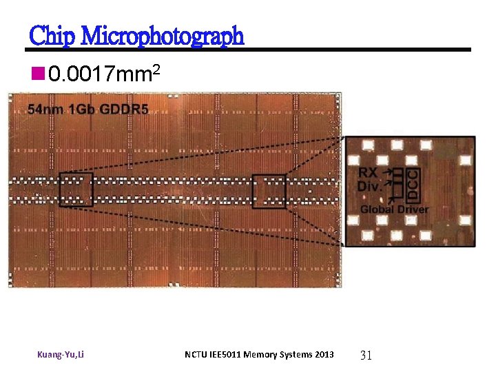
Chip Microphotograph n 0. 0017 mm 2 Kuang-Yu, Li NCTU IEE 5011 Memory Systems 2013 31

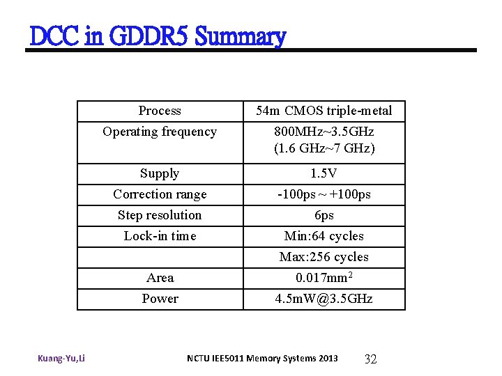
DCC in GDDR 5 Summary Process Operating frequency 54 m CMOS triple-metal 800 MHz~3. 5 GHz (1. 6 GHz~7 GHz) Supply Correction range Step resolution Lock-in time 1. 5 V -100 ps ~ +100 ps 6 ps Min: 64 cycles Max: 256 cycles 0. 017 mm 2 4. 5 m. W@3. 5 GHz Area Power Kuang-Yu, Li NCTU IEE 5011 Memory Systems 2013 32

Conclusion n Digital DCC in state of the art DRAM design is necessary and important n DCC in GDDR 5 with wide-range fast-lock duty-cycle corrector with offset-tolerant capability n WCK is up to 3. 5 GHz to sustain 7 Gbps/pin Kuang-Yu, Li NCTU IEE 5011 Memory Systems 2013 33
![Reference n n n 1 Kho R et al A 75 nm 7 Reference n n n [1] Kho, R , et. al, “A 75 nm 7](https://slidetodoc.com/presentation_image_h/7fd2c62dd9308f8b559dc40e180c207c/image-34.jpg)
Reference n n n [1] Kho, R , et. al, “A 75 nm 7 Gb/s/pin 1 Gb GDDR 5 Graphics Memory Device With Bandwidth Improvement Techniques”, IEEE Journal of Solid-State Circuits, vol. 45, no. 1 , pp 120 - 133, Jan. 2010 [2] L. Raghavan et. al, “Architectural Comparison of Analog and Digital Duty Cycle Corrector for High Speed I/O Link, ” VLSI Design, pp 270 -275, Jan. 2010 [3] Dongsuk Shin et. al, “A 7 ps-Jitter 0. 053 mm 2 Fast-Lock ADDLL with Wide-Range and High. Resolution All-Digital DCC”, ISSCC, pp 184 -185, Feb. 2007 [4] Shao-Ku Kao et. al, “All-Digital Fast-Locked Synchronous Duty-Cycle Corrector” IEEE Transactions on Circuits and Systems , vol. 53, pp 1363 - 1367, Dec. 2006 [5] Dongsuk Shin , Kwang-Jin Na et. al, “Wide-Range Fast-Lock Duty-Cycle Corrector with Offset. Tolerant Duty-Cycle Detection Scheme for 54 nm 7 Gb/s GDDR 5 DRAM Interface, ” Symposium on VLSI Circuits Digest of Technical Papers, pp 138 -139, June 2009 [6] Kyung Hoon Kim et. al, “A 5. 2 Gb/p/s GDDR 5 SDRAM with CML Clock Distribution Network”, ESSCIRC , pp 194 - 197, Sept. 2008 Kuang-Yu, Li NCTU IEE 5011 Memory Systems 2013 34