Identify that some electrons in solids are shared


- Slides: 5

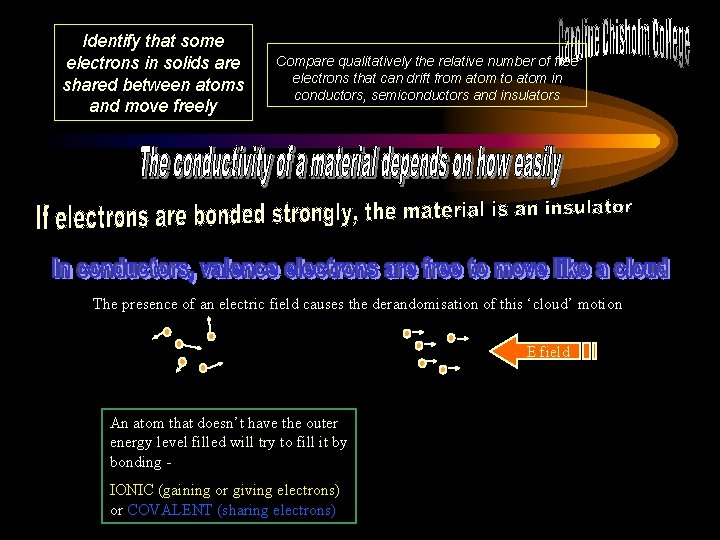
Identify that some electrons in solids are shared between atoms and move freely Compare qualitatively the relative number of free electrons that can drift from atom to atom in conductors, semiconductors and insulators The presence of an electric field causes the derandomisation of this ‘cloud’ motion E field An atom that doesn’t have the outer energy level filled will try to fill it by bonding IONIC (gaining or giving electrons) or COVALENT (sharing electrons)

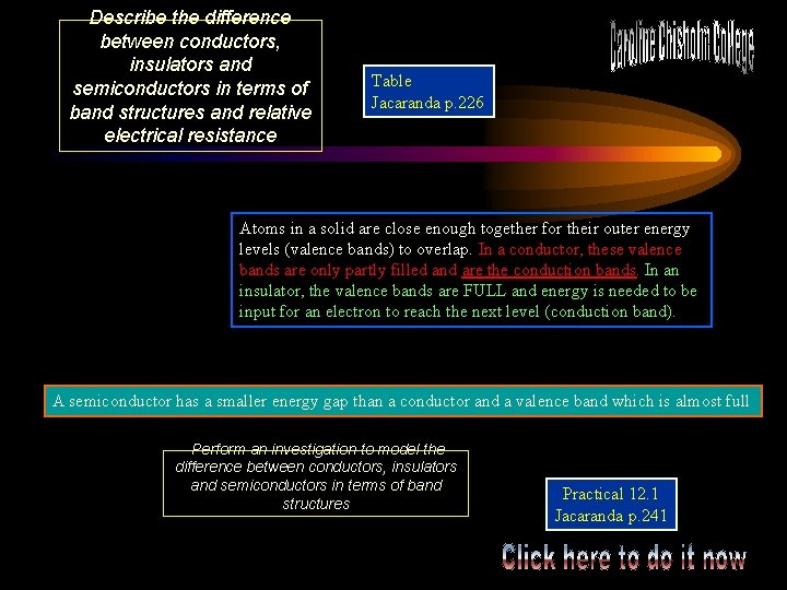
Describe the difference between conductors, insulators and semiconductors in terms of band structures and relative electrical resistance Table Jacaranda p. 226 Atoms in a solid are close enough together for their outer energy levels (valence bands) to overlap. In a conductor, these valence bands are only partly filled and are the conduction bands. In an insulator, the valence bands are FULL and energy is needed to be input for an electron to reach the next level (conduction band). A semiconductor has a smaller energy gap than a conductor and a valence band which is almost full Perform an investigation to model the difference between conductors, insulators and semiconductors in terms of band structures Practical 12. 1 Jacaranda p. 241

Identify absences of electrons in a nearly full band as holes, and recognise that both electrons and holes help to carry current This is because increasing temperature means that thermal energy causes electrons to jump the ‘gap’ into the conduction band. This leaves holes in the valence band, which move opposite to, and slower than, the electron flow. Perform an investigation to demonstrate a model for explaining the behaviour of semiconductors, including the creation of a hole or positive charge on the atom that has lost the electron and the movement of electrons and holes in opposite directions when an electric field is applied across the semiconductor DO try this at home!

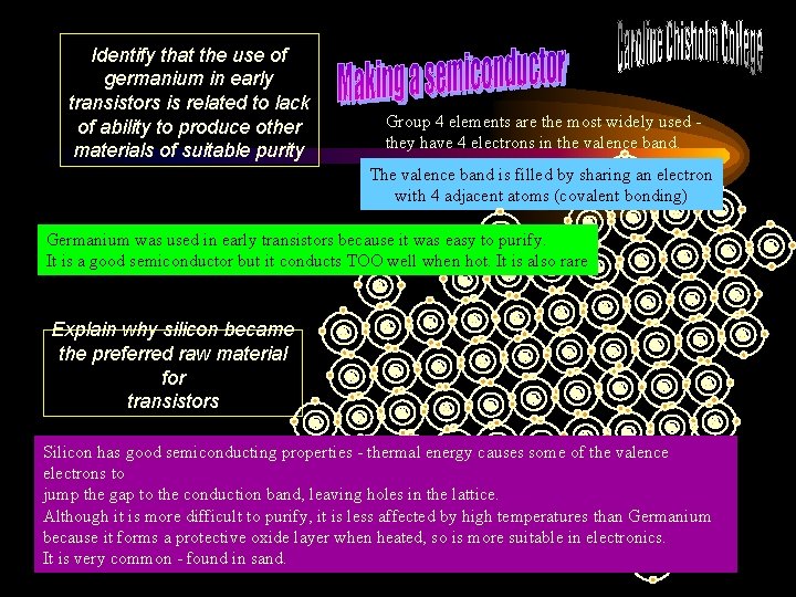
Identify that the use of germanium in early transistors is related to lack of ability to produce other materials of suitable purity Group 4 elements are the most widely used they have 4 electrons in the valence band. The valence band is filled by sharing an electron with 4 adjacent atoms (covalent bonding) Germanium was used in early transistors because it was easy to purify. It is a good semiconductor but it conducts TOO well when hot. It is also rare Explain why silicon became the preferred raw material for transistors Silicon has good semiconducting properties - thermal energy causes some of the valence electrons to jump the gap to the conduction band, leaving holes in the lattice. Although it is more difficult to purify, it is less affected by high temperatures than Germanium because it forms a protective oxide layer when heated, so is more suitable in electronics. It is very common - found in sand.

Describe how ‘doping’ a semiconductor can change its electrical properties ‘Dopant’ atoms in the semiconductor lattice can form extra energy levels in the gap - aiding conduction Doping is placing impurity atoms into the semiconductor crystal lattice to change the conductivity properties Identify differences in p and ntype semiconductors in terms of n-type p-type semiconductors have group 53 impurity atoms substituted the relative number of negative in in the lattice of of group 44 atoms charge carriers and positive Foreachimpurityatom, one For each impurity atom, one holes electron the electronmoves hole, orto electron moves topositive the nextcharge level -- -- the conduction carrier, is formed. Thisband. level the conduction band. This arrangement has excess negative arrangement has positive arrangement has excess negative chargeso sois called‘n-type’ ‘p-type’ charge so isiscalled ‘n-type’ Electrons move into the holes, creating new holes that other electrons move into, which makes other new holes etc. . . c M. Edwards 15/7/02 ELECTRON EXTRA HOLE! ELECTRON!