ICsemiconductorsICDOS Chee Wee Liu DistinguishedChair Professor IEEE Fellow

- Slides: 36

IC/semiconductors(IC+DOS) Chee Wee Liu (劉致為) Distinguished/Chair Professor / IEEE Fellow, National Taiwan University cliu@ntu. edu. tw http: //nanosioe. ee. ntu. edu. tw High mobility/High K 3 Dx 3 D DRAM/MRAM CIS/IGZO PPACR (performance, power, area, cost reliability) 1

• CVD磊晶為基礎,研發Si. Ge/Ge. Sn 元件、 stacked 3 D電晶體、MTJ/DRAM記憶體、 IGZO TFT、暨光電元件。 • 其優異的CVD磊晶技術,創下了矽電子遷 移率世界紀錄2, 400, 000 cm 2/Vs;並且將 CVD Ge. Sn通道的電洞遷移率超越MBE磊 晶。 • Ge及dislocation對strained Si (90 nm)產 生的flicker noise。 • 第一個stacked Ge. Si channel n. FET、 stacked Ge. Sn channel p. FET (2/1 nm) • 第一個Si/Si. Ge/Si. C MIS LED/detectors。 2

• 570多篇論文(含 228+期刊,25 IEDM及3 VLSI) • 38 US patents, 38 Taiwan ROC patents, 2 China patents • 5096次以上的論文被引用。 • 已畢業至少 34博士生和128碩士生,並現有15位 博士及10位碩士生。 • 畢業博士生有五位任教職(1 NTU, 1 NTNU, 1 NCHU, 1 NDHU及1 NJUST)及三位博後任教職(1 NTU, 1 NCU, 1 CGU)。 • NTU is the winner: TSMC/MTK/Intel/UMC/VG (Senior Director) • Graduate admission: Berkeley, MIT • US:coding 3

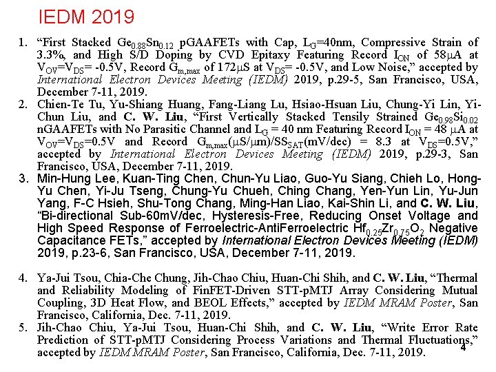
IEDM 2019 1. “First Stacked Ge 0. 88 Sn 0. 12 p. GAAFETs with Cap, LG=40 nm, Compressive Strain of 3. 3%, and High S/D Doping by CVD Epitaxy Featuring Record ION of 58 m. A at VOV=VDS= -0. 5 V, Record Gm, max of 172 m. S at VDS= -0. 5 V, and Low Noise, ” accepted by International Electron Devices Meeting (IEDM) 2019, p. 29 -5, San Francisco, USA, December 7 -11, 2019. 2. Chien-Te Tu, Yu-Shiang Huang, Fang-Liang Lu, Hsiao-Hsuan Liu, Chung-Yi Lin, Yi. Chun Liu, and C. W. Liu, “First Vertically Stacked Tensily Strained Ge 0. 98 Si 0. 02 n. GAAFETs with No Parasitic Channel and LG = 40 nm Featuring Record ION = 48 m. A at VOV=VDS=0. 5 V and Record Gm, max(m. S/mm)/SSSAT(m. V/dec) = 8. 3 at VDS=0. 5 V, ” accepted by International Electron Devices Meeting (IEDM) 2019, p. 29 -3, San Francisco, USA, December 7 -11, 2019. 3. Min-Hung Lee, Kuan-Ting Chen, Chun-Yu Liao, Guo-Yu Siang, Chieh Lo, Hong. Yu Chen, Yi-Ju Tseng, Chung-Yu Chueh, Ching Chang, Yen-Yun Lin, Yu-Jun Yang, F-C Hsieh, Shu-Tong Chang, Ming-Han Liao, Kai-Shin Li, and C. W. Liu, “Bi-directional Sub-60 m. V/dec, Hysteresis-Free, Reducing Onset Voltage and High Speed Response of Ferroelectric-Anti. Ferroelectric Hf 0. 25 Zr 0. 75 O 2 Negative Capacitance FETs, ” accepted by International Electron Devices Meeting (IEDM) 2019, p. 23 -6, San Francisco, USA, December 7 -11, 2019. 4. Ya-Jui Tsou, Chia-Che Chung, Jih-Chao Chiu, Huan-Chi Shih, and C. W. Liu, “Thermal and Reliability Modeling of Fin. FET-Driven STT-p. MTJ Array Considering Mutual Coupling, 3 D Heat Flow, and BEOL Effects, ” accepted by IEDM MRAM Poster, San Francisco, California, Dec. 7 -11, 2019. 5. Jih-Chao Chiu, Ya-Jui Tsou, Huan-Chi Shih, and C. W. Liu, “Write Error Rate Prediction of STT-p. MTJ Considering Process Variations and Thermal Fluctuations, ” 4 accepted by IEDM MRAM Poster, San Francisco, California, Dec. 7 -11, 2019.

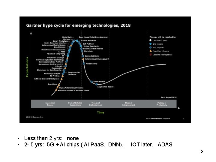
• Less than 2 yrs: none • 2 - 5 yrs: 5 G + AI chips ( AI Paa. S, DNN), IOT later, ADAS 5

Future: AI, Big Data, Connectivity(5 G/6 G) Hardware : IC/Semiconductor tsmc, MTK, APPLE Software: coding Google, MS, AMAZON, FB 6

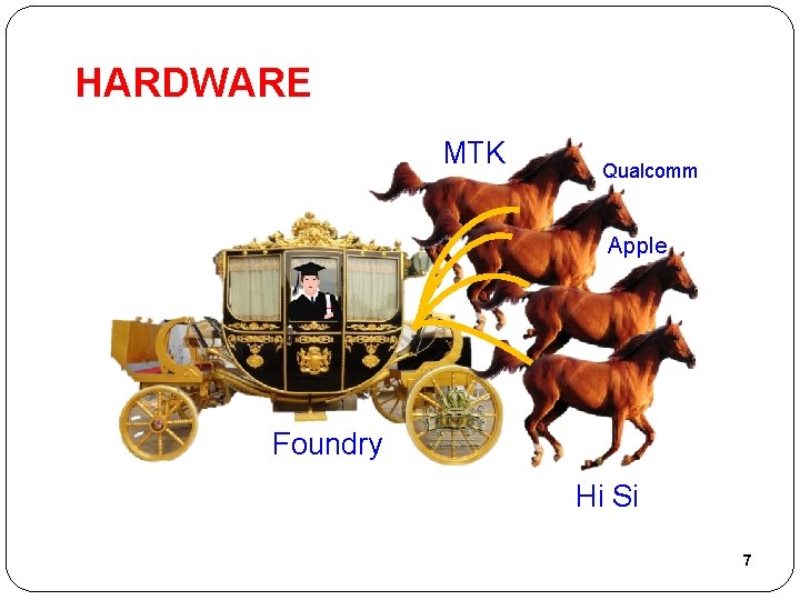
HARDWARE MTK Qualcomm Apple Foundry Hi Si 7


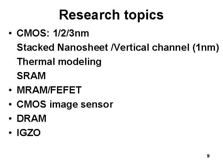
Research topics • CMOS: 1/2/3 nm Stacked Nanosheet /Vertical channel (1 nm) Thermal modeling SRAM • MRAM/FEFET • CMOS image sensor • DRAM • IGZO 9

Saturday 2 -4 pm free course • • • Free handout Free textbook Free schedule Cyclic No need to register for special project course • Welcome to join 2 -4 pm on Sat • Snacks, Pizza ? ? • Research involvement: 4000 -8000 NT

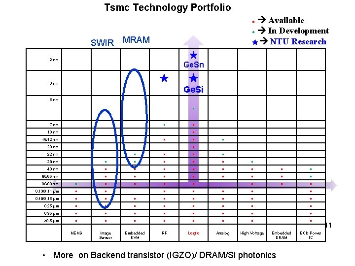
Tsmc Technology Portfolio Available ● In Development ★ NTU Research ● SWIR MRAM ★ Ge. Sn 2 nm ★ 3 nm ★ Ge. Si 5 nm ● 7 nm ● 10 nm ● ● 16/12 nm ● 20 nm ● ● ● 22 nm ● ● 28 nm ● ● ● 40 nm ● ● ● ● 65/55 nm ● ● 90/80 nm ● ● ● 0. 13/0. 11 μm ● ● ● ● 0. 18/0. 15 μm ● ● ● ● 0. 25 μm ● ● ● ● 0. 35 μm ● ● ● ● >0. 5 μm ● ● ● ● MEMS Image Sensor Embedded NVM RF Logic Analog High Voltage Embedded DRAM • More on Backend transistor (IGZO)/ DRAM/Si photonics BCD-Power IC 11

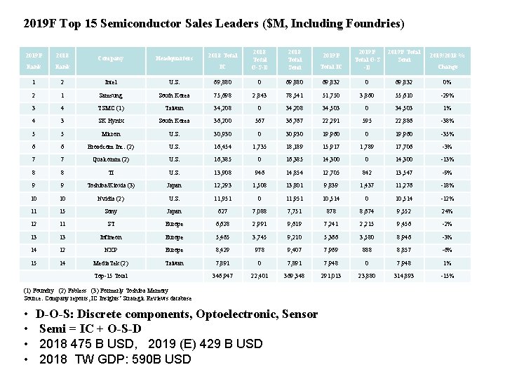
2019 F Top 15 Semiconductor Sales Leaders ($M, Including Foundries) IC 2018 Total O-S-D 2018 Total Semi 2019 F Total Semi 2019/2018 % Total IC 2019 F Total O-S -D U. S. 69, 880 0 69, 880 69, 832 0% Samsung South Korea 75, 698 2, 843 78, 541 51, 750 3, 860 55, 610 -29% 4 TSMC (1) Taiwan 34, 208 0 34, 208 34, 503 0 34, 503 1% 4 3 SK Hynix South Korea 36, 200 567 36, 767 22, 291 595 22, 886 -38% 5 5 Micron U. S. 30, 930 0 30, 930 19, 960 -35% 6 6 Broadcom Inc. (2) U. S. 16, 454 1, 735 18, 189 15, 917 1, 789 17, 706 -3% 7 7 Qualcomm (2) U. S. 16, 385 0 16, 385 14, 300 0 14, 300 -13% 8 8 TI U. S. 13, 908 946 14, 854 12, 705 842 13, 547 -9% 9 9 Toshiba/Kioxia (3) Japan 12, 293 1, 508 13, 801 9, 839 1, 437 11, 276 -18% 10 10 Nvidia (2) U. S. 11, 951 0 11, 951 10, 514 0 10, 514 -12% 11 15 Sony Japan 627 7, 088 7, 751 878 8, 674 9, 552 24% 12 11 ST Europe 6, 628 2, 991 9, 619 7, 241 2, 215 9, 456 -2% 13 13 Infineon Europe 5, 465 3, 745 9, 210 5, 366 3, 580 8, 946 -3% 14 12 NXP Europe 8, 429 978 9, 407 7, 969 888 8, 857 -6% 15 14 Media. Tek (2) Taiwan 7, 891 0 7, 891 7, 948 0 7, 948 1% 346, 947 22, 401 369, 348 291, 013 23, 880 314, 893 -15% 2019 F 2018 Rank 1 2 Intel 2 1 3 Company Headquarters Top-15 Total 2018 Total 2019 F (1) Foundry (2) Fabless (3) Formerly Toshiba Memory Source: Company reports, IC Insights’ Strategic Reviews database • • D-O-S: Discrete components, Optoelectronic, Sensor Semi = IC + O-S-D 2018 475 B USD, 2019 (E) 429 B USD 2018 TW GDP: 590 B USD Change

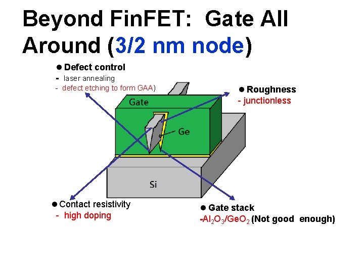
Beyond Fin. FET: Gate All Around (3/2 nm node) l Defect control - laser annealing - defect etching to form GAA) l Contact resistivity - high doping l Roughness - junctionless l Gate stack -Al 2 O 3/Ge. O 2 (Not good enough)

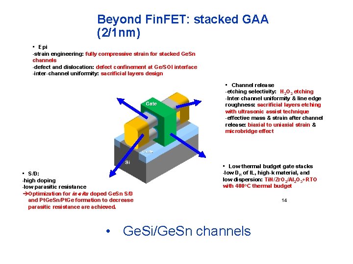
Beyond Fin. FET: stacked GAA (2/1 nm) • Epi -strain engineering: fully compressive strain for stacked Ge. Sn channels -defect and dislocation: defect confinement at Ge/SOI interface -inter-channel uniformity: sacrificial layers design • Channel release -etching selectivity: H 2 O 2 etching -Inter-channel uniformity & line edge roughness: sacrificial layers etching with ultrasonic assist technique -effective mass & strain after channel release: biaxial to uniaxial strain & microbridge effect • S/D: -high doping -low parasitic resistance èOptimization for in-situ doped Ge. Sn S/D and Pt. Ge. Sn/Pt. Ge formation to decrease parasitic resistance are achieved. • Low thermal budget gate stacks -low Dit of IL, high-k material, and low dispersion: Ti. N/Zr. O 2/Al 2 O 3+RTO with 400 o. C thermal budget • Ge. Si/Ge. Sn channels 14

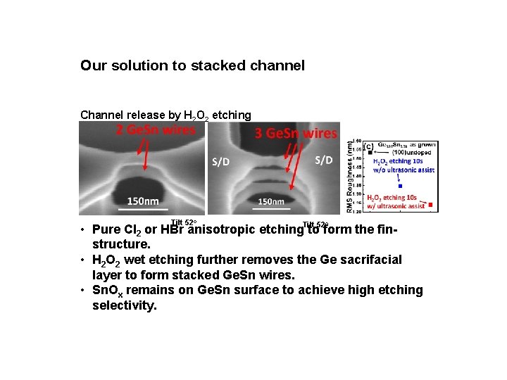
Our solution to stacked channel Channel release by H 2 O 2 etching Tilt 52 o Tilt 52 • Pure Cl 2 or HBr anisotropic etching to form the finstructure. • H 2 O 2 wet etching further removes the Ge sacrifacial layer to form stacked Ge. Sn wires. • Sn. Ox remains on Ge. Sn surface to achieve high etching selectivity. o

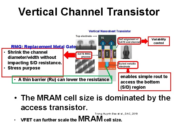
Vertical Channel Transistor Vertical Nanosheet Transistor Variability control RMG: Replacement Metal Gate • Shrink the channel diameter/width without impacting S/D resistance. • Stress purpose • A thin barrier (Ru) can lower the resistance enables simple rout to access the bottom (S/D) region • The MRAM cell size is dominated by the access transistor. • VFET can further scale the MRAM cell size. Trong Huynh-Bao et al. , DAC, 2019

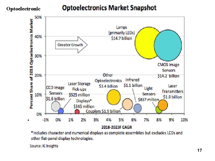
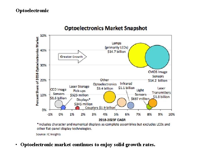
Optoelectronic • Optoelectronic market continues to enjoy solid growth rates. 17

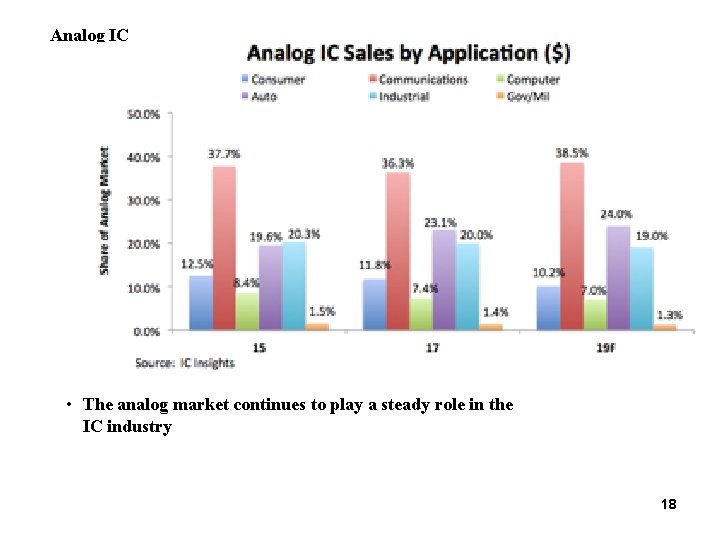
Analog IC • The analog market continues to play a steady role in the IC industry 18

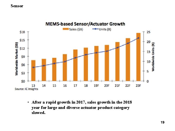
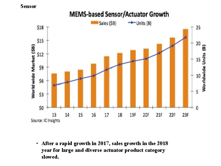
Sensor • After a rapid growth in 2017, sales growth in the 2018 year for large and diverse actuator product category slowed. 19

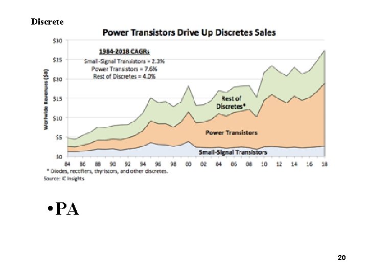
Discrete • PA 20

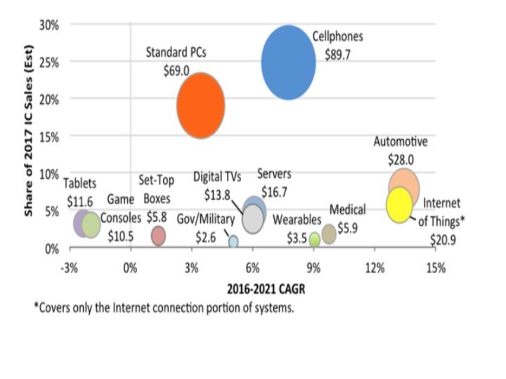
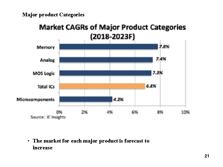
Major product Categories • The market for each major product is forecast to increase 21

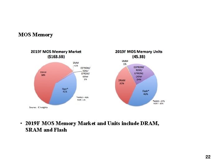
MOS Memory • 2019 F MOS Memory Market and Units include DRAM, SRAM and Flash 22

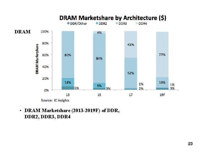
DRAM • DRAM Marketshare (2013 -2019 F) of DDR, DDR 2, DDR 3, DDR 4 23

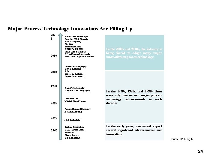
Major Process Technology Innovations Are Pilling Up 202 0 2010 2000 1990 1980 Nanocarbon Technologies Ge and/or III-V Channels EUV Lithography Air Gaps Thru-Silicon Vias ETSOI (or FD-SOI) Multi-Gate Transistors DP and Inverse Lithography Metal Gates/High-k Gate Oxides In the 2000 s and 2010 s, the industry is being forced to adopt many major innovations in process technology. Immersion Lithography Low-K Insulators Si. Ge Silicon-on-Insulator Copper Interconnects Deep UV Lithography Step-and-Scan Lithography CMP and STI Multiple Metal Layers In the 1970 s, 1980 s, and 1990 s there were only one or two major process technology advancements in each decade. Step-and-Repeat Lithography Projection Printing 1970 1960 Ion Implantation Surface Passivation CMOS Architecture MOSFET Planar Process Oxide Masking In the early years, one would expect several significant advancements and innovations. Source: IC Insights 24

Optoelectronic • Optoelectronic market continues to enjoy solid growth rates.

Sensor • After a rapid growth in 2017, sales growth in the 2018 year for large and diverse actuator product category slowed.

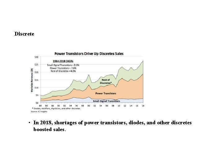
Discrete • In 2018, shortages of power transistors, diodes, and other discretes boosted sales.

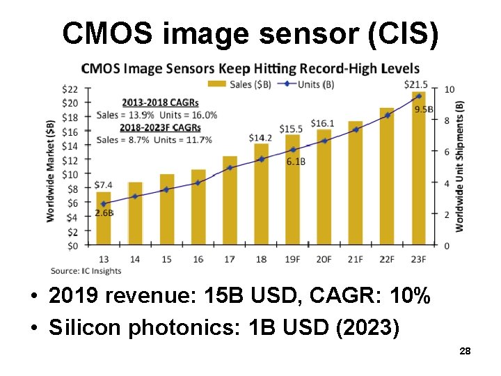
CMOS image sensor (CIS) • 2019 revenue: 15 B USD, CAGR: 10% • Silicon photonics: 1 B USD (2023) 28

Applications • Night vision: 850 nm, 940 nm, 1310 nm, 1550 nm • Face ID: 940 nm, 1550 nm • Lidar: 850/905 nm, 1550 nm (high speed) • 現在silicon到 940 nm, 未來用Ge • Ge/Ge. Si/Ge. Sn epi/detector/sensor array 29

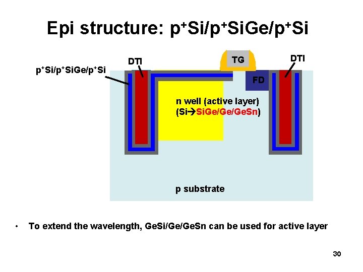
Epi structure: p+Si/p+Si. Ge/p+Si DTI TG DTI FD n well (active layer) (Si Si. Ge/Ge/Ge. Sn) DTI p substrate • To extend the wavelength, Ge. Si/Ge/Ge. Sn can be used for active layer 30

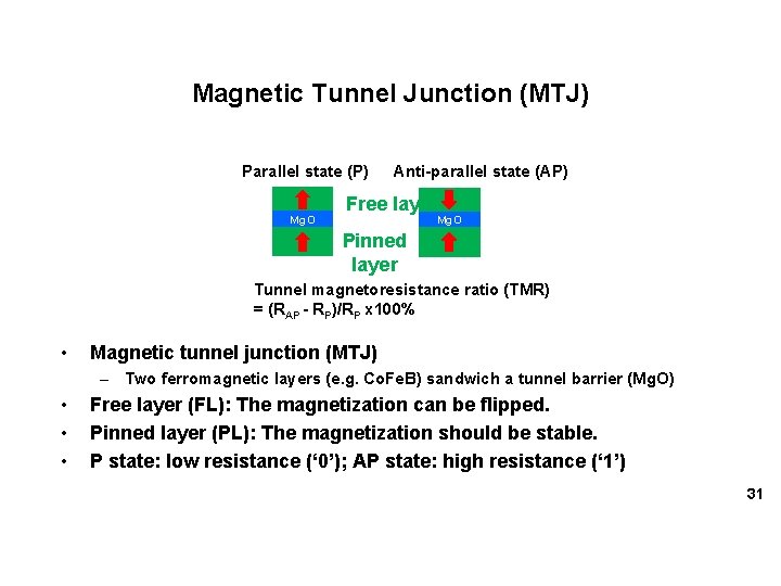
Magnetic Tunnel Junction (MTJ) Parallel state (P) Mg. O Anti-parallel state (AP) Free layer Mg. O Pinned layer Tunnel magnetoresistance ratio (TMR) = (RAP - RP)/RP x 100% • Magnetic tunnel junction (MTJ) – Two ferromagnetic layers (e. g. Co. Fe. B) sandwich a tunnel barrier (Mg. O) • • • Free layer (FL): The magnetization can be flipped. Pinned layer (PL): The magnetization should be stable. P state: low resistance (‘ 0’); AP state: high resistance (‘ 1’) 31

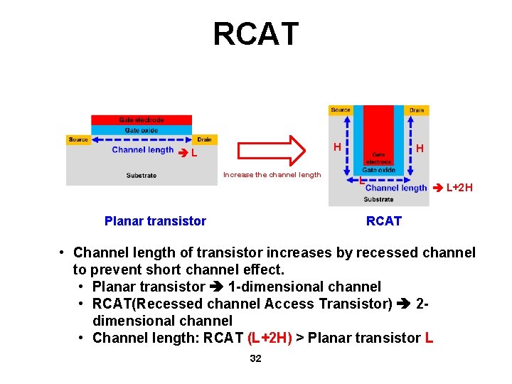
RCAT H L Increase the channel length Planar transistor H L L+2 H RCAT • Channel length of transistor increases by recessed channel to prevent short channel effect. • Planar transistor 1 -dimensional channel • RCAT(Recessed channel Access Transistor) 2 dimensional channel • Channel length: RCAT (L+2 H) > Planar transistor L 32

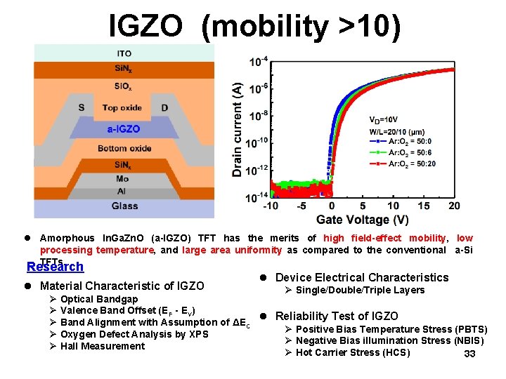
IGZO (mobility >10) l Amorphous In. Ga. Zn. O (a-IGZO) TFT has the merits of high field-effect mobility, low processing temperature, and large area uniformity as compared to the conventional a-Si TFTs. Research l Material Characteristic of IGZO l Device Electrical Characteristics Ø Single/Double/Triple Layers Ø Optical Bandgap Ø Valence Band Offset (EF - EV) l Reliability Test of IGZO Ø Band Alignment with Assumption of ΔEC Ø Positive Bias Temperature Stress (PBTS) Ø Oxygen Defect Analysis by XPS Ø Negative Bias illumination Stress (NBIS) Ø Hall Measurement Ø Hot Carrier Stress (HCS) 33

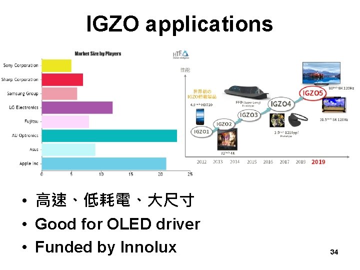
IGZO applications • 高速、低耗電、大尺寸 • Good for OLED driver • Funded by Innolux 34

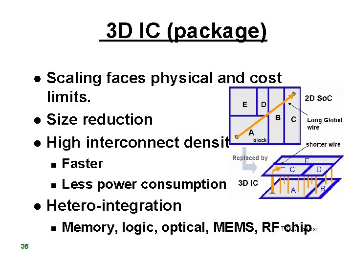
3 D IC (package) l l l Scaling faces physical and cost limits. Size reduction High interconnect density n n l Hetero-integration n 35 Faster Less power consumption TSMC course Memory, logic, optical, MEMS, RF chip

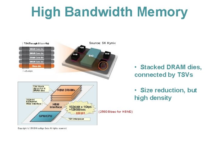
High Bandwidth Memory Source: SK Hynix • Stacked DRAM dies, connected by TSVs • Size reduction, but high density HBM 1 (256 GB/sec for HBM 2)