
IC Workshop Summary InDetector Electronics Challenges Gunther Haller
- Slides: 19
IC Workshop Summary & In-Detector Electronics Challenges Gunther Haller Community Summer Study 2013, U. Minnesota Instrumentation Frontier Session July 31, 2013
IC Workshop Summary • A workshop titled “US Workshop on IC Design for High Energy Physics – HEPIC 2013” was held May 30 to June 1, 2013 at LBNL. • The motivation, agenda, presentations, and list of attendees are posted at the following location: https: //indico. physics. lbl. gov/indico/conference. Display. py? c onf. Id=2 • Report posted on CSS web-site. 2
Workshop scope • The scope of the whitepaper includes the following topics: • Needs for IC technologies to enable future experiments in the three HEP frontiers – Energy, Cosmic and Intensity Frontiers. • Challenges in the different technology and circuit design areas and the related R&D needs. • Motivation for using different fabrication technologies. • Outlook of future technologies including 2. 5 D and 3 D. • Survey of IC’s used in current experiments and IC’s targeted for approved or proposed experiments. • IC design at US institutes and recommendations for collaboration in the future. 3
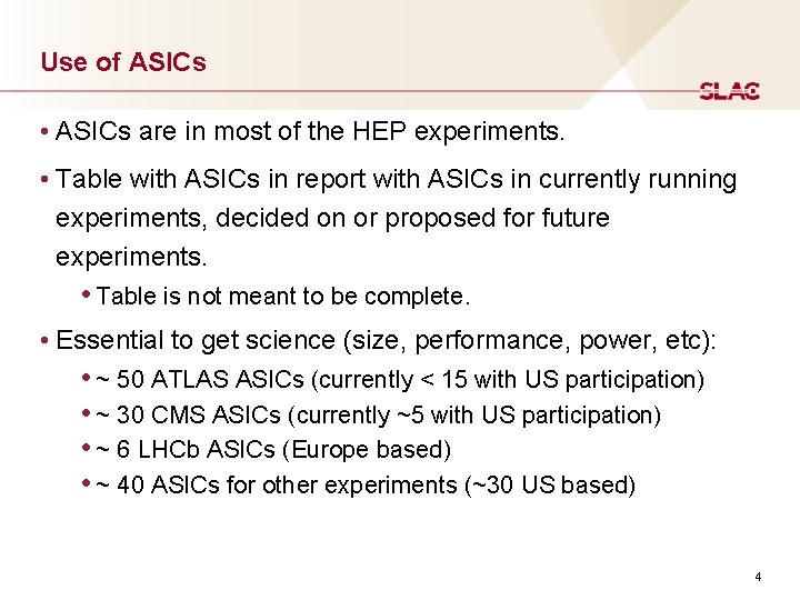
Use of ASICs • ASICs are in most of the HEP experiments. • Table with ASICs in report with ASICs in currently running experiments, decided on or proposed for future experiments. • Table is not meant to be complete. • Essential to get science (size, performance, power, etc): • ~ 50 ATLAS ASICs (currently < 15 with US participation) • ~ 30 CMS ASICs (currently ~5 with US participation) • ~ 6 LHCb ASICs (Europe based) • ~ 40 ASICs for other experiments (~30 US based) 4
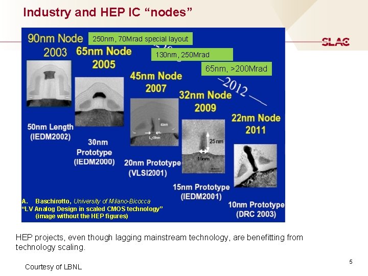
Industry and HEP IC “nodes” 250 nm, 70 Mrad special layout 130 nm, 250 Mrad 65 nm, >200 Mrad A. Baschirotto, University of Milano-Bicocca “LV Analog Design in scaled CMOS technology” (image without the HEP figures) HEP projects, even though lagging mainstream technology, are benefitting from technology scaling. Courtesy of LBNL 5
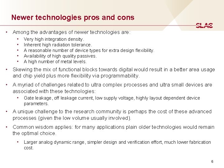
Newer technologies pros and cons • Among the advantages of newer technologies are: • • • Very high integration density. Inherent high radiation tolerance. A reasonable number of device types for extra design flexibility. Availability of high quality passives. A high number of metal levels. • Skewing the mix of functional blocks towards digital would result in a better area usage and chip yield plus more flexibility via programmability. • A myriad of challenges related to ultra complex processes and ultra small devices are associated with these technologies: • Gate leakage, off leakage current, low supply voltage, highly layout dependent device parameters. • A unique challenge to the research community is perhaps the cost of these advanced processes (given the low volume usually involved). • Common wisdom applies: for many applications plain older technologies would remain the optimal choice. • Larger analog dynamic range, simpler design and verification effort, much lower fabrication cost. 6
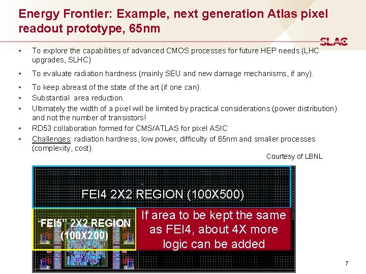
Energy Frontier: Example, next generation Atlas pixel readout prototype, 65 nm • To explore the capabilities of advanced CMOS processes for future HEP needs (LHC upgrades, SLHC) • To evaluate radiation hardness (mainly SEU and new damage mechanisms, if any). • • • To keep abreast of the state of the art (if one can). Substantial area reduction. Ultimately the width of a pixel will be limited by practical considerations (power distribution) and not the number of transistors! RD 53 collaboration formed for CMS/ATLAS for pixel ASIC Challenges: radiation hardness, low power, difficulty of 65 nm and smaller processes (complexity, cost). • • Courtesy of LBNL FEI 4 2 X 2 REGION (100 X 500) If area to be kept the same “FEI 5” 2 X 2 REGION as FEI 4, about 4 X more (100 X 200) logic can be added 7
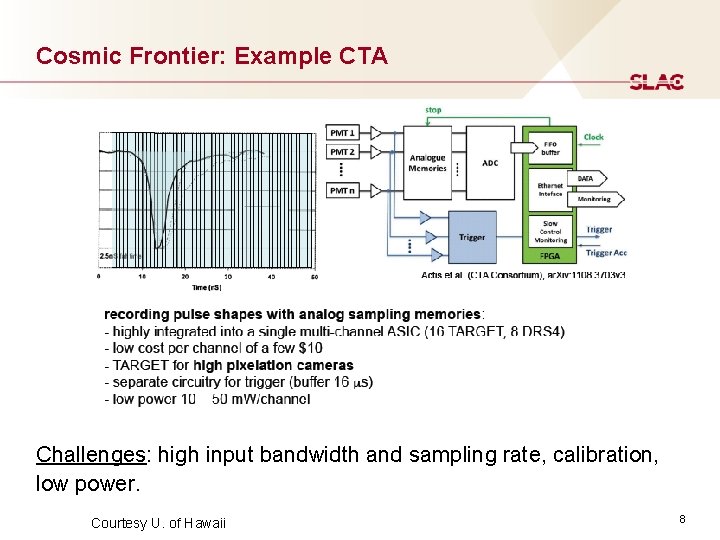
Cosmic Frontier: Example CTA Challenges: high input bandwidth and sampling rate, calibration, low power. Courtesy U. of Hawaii 8
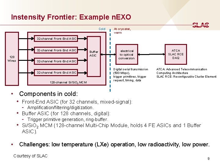
Instensity Frontier: Example n. EXO Cold At cryostat, warm 32 -channel Front-End ASIC 128 Wires Buffer ASIC 32 -channel Front-End ASIC 128 -channel Si/Si. O 2 MCM electrical to optical conversion Digital serial transmission (500 Mbps), trigger primitives, trigger request, timing, data ATCA SLAC RCE DAQ ATCA: Advanced Telecommunication Computing Architecture SLAC RCE: Reconfigurable Cluster Element • Components in cold: • Front-End ASIC (for 32 channels, mixed-signal): - Amplification/filtering/digitization. • Buffer ASIC (for 128 channels, digital): - Trigger primitive generation, ring-buffer. • Si/Si. O 2 MCM (128 -channel Multi-Chip Module, holds 4 FE ASICs and 1 Buffer ASIC). • Challenges: low temperature (LXe) operation, low radioactivity, low power. Courtesy of SLAC 9
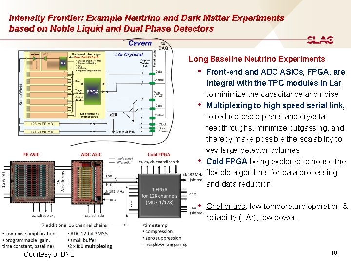
Intensity Frontier: Example Neutrino and Dark Matter Experiments based on Noble Liquid and Dual Phase Detectors Long Baseline Neutrino Experiments • Front-end and ADC ASICs, FPGA, are • • integral with the TPC modules in Lar, to minimize the capacitance and noise Multiplexing to high speed serial link, to reduce cable plants and cryostat feedthroughs, minimize outgassing, and thereby make possible the scalability to vey large detector volumes Cold FPGA being explored to house the flexible algorithms for data processing and data reduction • Challenges: low temperature operation & reliability (LAr), low power. Courtesy of BNL 10
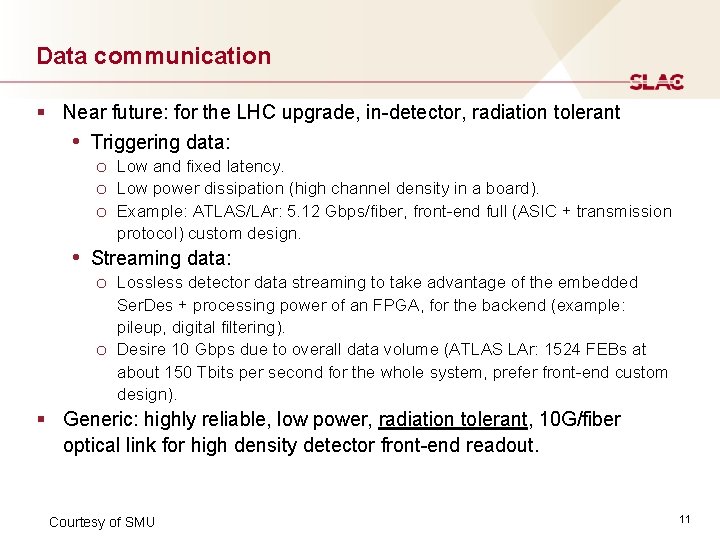
Data communication § Near future: for the LHC upgrade, in-detector, radiation tolerant • Triggering data: o Low and fixed latency. o Low power dissipation (high channel density in a board). o Example: ATLAS/LAr: 5. 12 Gbps/fiber, front-end full (ASIC + transmission protocol) custom design. • Streaming data: o Lossless detector data streaming to take advantage of the embedded o Ser. Des + processing power of an FPGA, for the backend (example: pileup, digital filtering). Desire 10 Gbps due to overall data volume (ATLAS LAr: 1524 FEBs at about 150 Tbits per second for the whole system, prefer front-end custom design). § Generic: highly reliable, low power, radiation tolerant, 10 G/fiber optical link for high density detector front-end readout. Courtesy of SMU 11
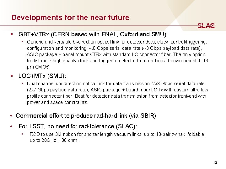
Developments for the near future § GBT+VTRx (CERN based with FNAL, Oxford and SMU). • Generic and versatile bi-direction optical link for detector data, clock, control/triggering, configuration and monitoring. 4. 8 Gbps serial data rate (~3 Gbps payload data rate), ASIC package + panel mount VTRx with standard LC connector fiber. The only option to distribute high quality clock and trigger to detector front-end in rad-environment. 0. 13 μm CMOS. § LOC+MTx (SMU): • Dual channel uni-direction optical link for data transmission. 2 x 8 Gbps serial data rate (2 x 7 Gbps payload data rate), ASIC package + board mount MTx with custom ultra low profile connector fiber. Best for detector data transmission from detector front-end with power and space constraints. • Commercial effort to produce rad-hard link (via SBIR) • For LSST, no need for rad-tolerance (SLAC): • R&D to use 3 M ribbon for shorter length vacuum links, up to 18 -pair twinax, foldable, up to 20 GHz, 100 ohm. 12
More generic communication R&D § Array optics based (SMU, OSU). • Custom driver ASIC + optical transmitter module based on mechanical parts from industry. • Aiming for 10 Gbps/fiber and 120 Gbps/module. • Preliminary ASIC prototypes exist. § Free space (FNAL, ANL). • For special applications such as in silicon tracker where it has a tight material budget. § External modulation (UMN, ANL): • Compact, less power, support high bandwidth (> 10 Gbps) • (ANL) Investigating COTS 10 GB/s modulators built based on Li. Nb. O 3, In. P, and Si. Not radiation • tolerant due to the embedded micro controller in the circuits. Difficult to work with industry to customize their designs. (UMN) Thin film Barium Strontium Titanate (BSTO) has been grown on Si substrates by codeposition of raw metals in oxygen. Its electro/opto property investigation and waveguide design are on-going. Many years to application. • In general: main reason for R&D on communication links is because of radiation tolerant requirements • Industry is much better in non-rad tolerant links, uses much small feature size processes, faster, lower power 13
Findings from workshop • Use of ASICs is often critical to enable an experiment, but even for experiments that could be done without ASICs, use of ASICs generally leads to improved performance and reliability. • ASICs will be necessary for essentially all detector subsystems at the HL-LHC. • Most or all intensity frontier experiments will need ASICs, even if the needs of some • experiments are not yet well developed. Even ground based cosmic frontier experiments will need ASICs to manage ever larger channel counts and meet several other requirements including performance. • It was recognized that the science enabled by IC developments has been impressive. • Yet most of these developments have been incremental (not surprisingly as in the microelectronics industry). • Close communication between physicists and IC designers is essential for successful development of new IC's. • Developing IC's from specifications, without interaction leading to optimization, does not work. • HEP has spearheaded the use of ASICs, but there is a growing need and adoption by other disciplines- not only Nuclear Physics which has a close connection to HEP, but also BES. 14
Findings from workshop con’t • ASIC design capability in the US HEP community is not concentrated in one location, but rather spread over several laboratories and universities. • It is essential because it facilitates the necessary intimate connection between detector designers and ASIC designers. This is especially important for front-end electronics, where the creative tension between the desirable, the possible, and the affordable is a key element of the design process. • Training of engineers and physicists at universities for HEP should include an understanding of the capabilities and limitations of ASICs given their importance in modern experiments. • R&D is needed to evaluate new technologies for their suitability for HEP, to develop new device structures, and to improve the performance for future experiments. • It is important to keep pace with industry technology development. However, more modern processes are increasingly more complex. • The design manual for 65 nm CMOS is more than 3 times the size of the manual for 130 nm. Mastering new processes demands increasingly more effort from IC design groups. 15
Findings from workshop con’t • Most ASICs in HEP are currently designed in 250 nm and 130 nm technology. • It seems that 250 nm technology will be offered for at least 10 more years, and 130 nm technology even longer. • Some applications benefit from smaller feature sizes. • Multi-project fabrication services as provided by MOSIS (US) or Europractice (Europe) are essential to substantially reduce the cost of prototype circuits. • CERN provides prototyping access to the world-wide HEP community (including the US) for specific processes suitable for the radiation environment at LHC. • CERN plans for future support continue to be generously inclusive. • Finding ways to balance designer work load as projects end and new ones begin was a serious concern of all groups, both labs and universities. • All groups develop ASICs for non-HEP research, such as BES, and this provides some level of load balancing, but may not be enough especially for smaller groups. • The main barrier against a designer at institute A working a small fraction of time on a project from institute B seems to be bureaucracy preventing institute B from paying for design time at institute A in a simple way. • For large projects, funding agreements or work for others contracts are set up, but the paperwork involved is too large and too slow for small jobs and the overhead costs are prohibitive for smaller groups including universities. 16
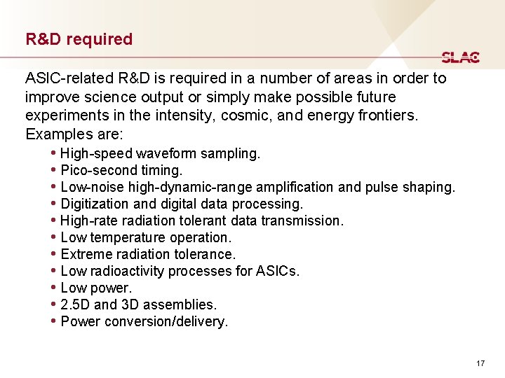
R&D required ASIC-related R&D is required in a number of areas in order to improve science output or simply make possible future experiments in the intensity, cosmic, and energy frontiers. Examples are: • High-speed waveform sampling. • Pico-second timing. • Low-noise high-dynamic-range amplification and pulse shaping. • Digitization and digital data processing. • High-rate radiation tolerant data transmission. • Low temperature operation. • Extreme radiation tolerance. • Low radioactivity processes for ASICs. • Low power. • 2. 5 D and 3 D assemblies. • Power conversion/delivery. 17
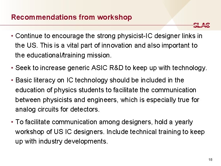
Recommendations from workshop • Continue to encourage the strong physicist-IC designer links in the US. This is a vital part of innovation and also important to the educational/training mission. • Seek to increase generic ASIC R&D to keep up with technology. • Basic literacy on IC technology should be included in the education of physics students to facilitate the communication between physicists and engineers, which is especially true for analog circuits for detectors. • To facilitate communication among designers, hold a yearly workshop of US IC designers. Include technical training to keep up with industry developments. 18
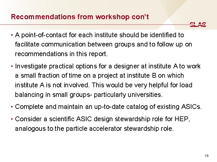
Recommendations from workshop con’t • A point-of-contact for each institute should be identified to facilitate communication between groups and to follow up on recommendations in this report. • Investigate practical options for a designer at institute A to work a small fraction of time on a project at institute B on which institute A is not involved. This would be very helpful for load balancing in small groups- particularly universities. • Complete and maintain an up-to-date catalog of existing ASICs. • Consider a scientific ASIC design stewardship role for HEP, analogous to the particle accelerator stewardship role. 19