IAY 0600 DIGITAL SYSTEMS DESIGN Digital Systems Design
![Full Custom ASICs [1] development from scratch complete control over each layer may include Full Custom ASICs [1] development from scratch complete control over each layer may include](https://slidetodoc.com/presentation_image_h2/229443b92688f5e4346ec41ee2ba6f08/image-5.jpg)
![Gate array ASICs [2] basic cells are premanufactured only connections are needed fabrication is Gate array ASICs [2] basic cells are premanufactured only connections are needed fabrication is](https://slidetodoc.com/presentation_image_h2/229443b92688f5e4346ec41ee2ba6f08/image-6.jpg)
![Standard cells ASICs [2] standard cells are predesigned finding optimal placement and routing is Standard cells ASICs [2] standard cells are predesigned finding optimal placement and routing is](https://slidetodoc.com/presentation_image_h2/229443b92688f5e4346ec41ee2ba6f08/image-7.jpg)
![Structured ASICs [3] premanufactured base tiles/modules and RAMs, PLLs, clock trees, etc. only connections Structured ASICs [3] premanufactured base tiles/modules and RAMs, PLLs, clock trees, etc. only connections](https://slidetodoc.com/presentation_image_h2/229443b92688f5e4346ec41ee2ba6f08/image-8.jpg)
![Simple programmable logic device [3] n Programmable logic array (PLA) allows Sum of Products Simple programmable logic device [3] n Programmable logic array (PLA) allows Sum of Products](https://slidetodoc.com/presentation_image_h2/229443b92688f5e4346ec41ee2ba6f08/image-10.jpg)
![Complex programmable logic device [4] Cool. Runner-II CPLD Family Data Sheet, DS 090 (v Complex programmable logic device [4] Cool. Runner-II CPLD Family Data Sheet, DS 090 (v](https://slidetodoc.com/presentation_image_h2/229443b92688f5e4346ec41ee2ba6f08/image-11.jpg)
![Conceptual structure of an FPGA [5] Chu, P. P. (2008) References, in FPGA Prototyping Conceptual structure of an FPGA [5] Chu, P. P. (2008) References, in FPGA Prototyping](https://slidetodoc.com/presentation_image_h2/229443b92688f5e4346ec41ee2ba6f08/image-13.jpg)
![Three-input LUT-based logic cell [5] Chu, P. P. (2008) References, in FPGA Prototyping by Three-input LUT-based logic cell [5] Chu, P. P. (2008) References, in FPGA Prototyping by](https://slidetodoc.com/presentation_image_h2/229443b92688f5e4346ec41ee2ba6f08/image-14.jpg)
![Three-input Look. Up Table (LUT) (1) [3] Clive Maxfield. (2004) The Design Warrior's Guide Three-input Look. Up Table (LUT) (1) [3] Clive Maxfield. (2004) The Design Warrior's Guide](https://slidetodoc.com/presentation_image_h2/229443b92688f5e4346ec41ee2ba6f08/image-15.jpg)
![Nexys-3 FPGA Board (1) [6] n Nexys-3 FPGA board features: Xilinx Spartan-6 XC 6 Nexys-3 FPGA Board (1) [6] n Nexys-3 FPGA board features: Xilinx Spartan-6 XC 6](https://slidetodoc.com/presentation_image_h2/229443b92688f5e4346ec41ee2ba6f08/image-49.jpg)
![Nexys-3 FPGA Board (2) [6] Nexys 3 FPGA Board Reference Manual, Digilent Inc. , Nexys-3 FPGA Board (2) [6] Nexys 3 FPGA Board Reference Manual, Digilent Inc. ,](https://slidetodoc.com/presentation_image_h2/229443b92688f5e4346ec41ee2ba6f08/image-50.jpg)
- Slides: 50

IAY 0600 DIGITAL SYSTEMS DESIGN Digital Systems Design Overwiev IAY 0600 Course Labs` Organization XILINX ISE Design Suite Overwiev Dmitri Mihhailov Tallinn University of Technology

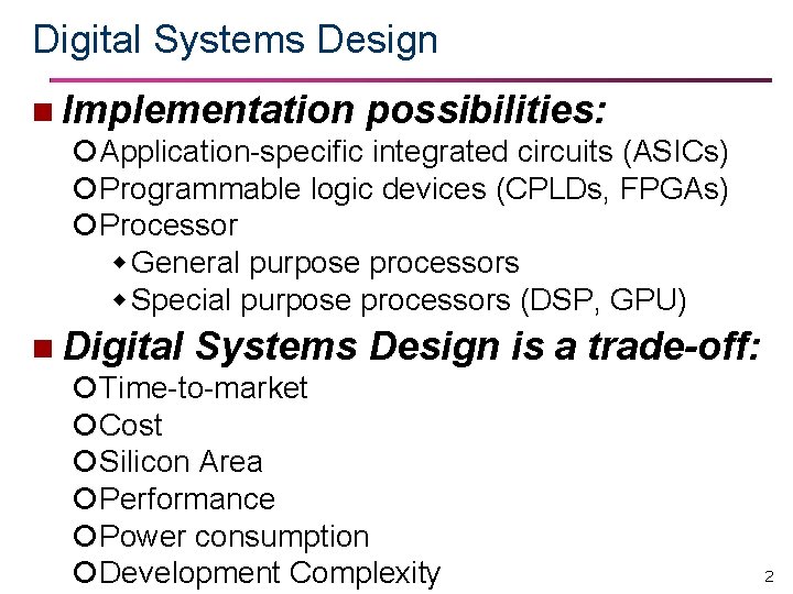
Digital Systems Design n Implementation possibilities: Application-specific integrated circuits (ASICs) Programmable logic devices (CPLDs, FPGAs) Processor General purpose processors Special purpose processors (DSP, GPU) n Digital Systems Design Time-to-market Cost Silicon Area Performance Power consumption Development Complexity is a trade-off: 2

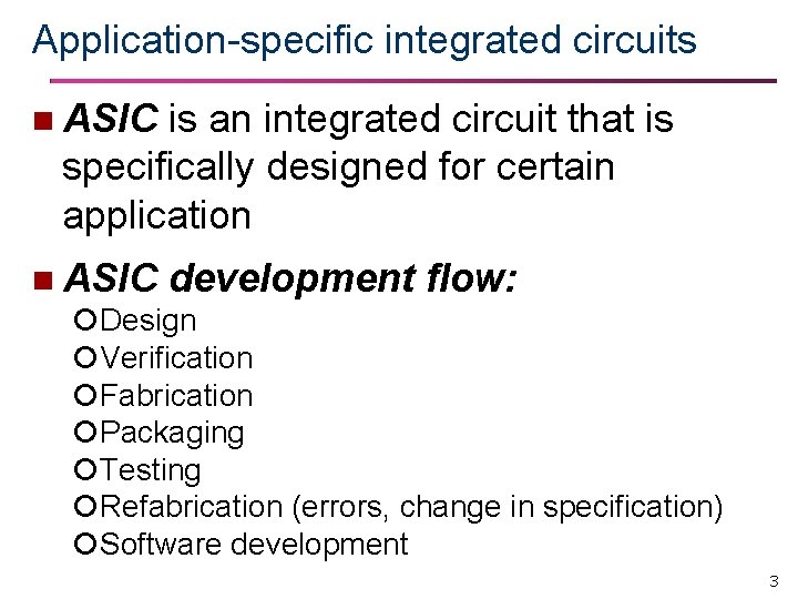
Application-specific integrated circuits n ASIC is an integrated circuit that is specifically designed for certain application n ASIC development flow: Design Verification Fabrication Packaging Testing Refabrication (errors, change in specification) Software development 3

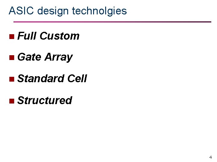
ASIC design technolgies n Full Custom n Gate Array n Standard Cell n Structured 4
![Full Custom ASICs 1 development from scratch complete control over each layer may include Full Custom ASICs [1] development from scratch complete control over each layer may include](https://slidetodoc.com/presentation_image_h2/229443b92688f5e4346ec41ee2ba6f08/image-5.jpg)
Full Custom ASICs [1] development from scratch complete control over each layer may include analog circuitry special tools highly complex and time consuming allows highest optimization [1] https: //en. wikipedia. org/wiki/Application-specific_integrated_circuit#Full 5 custom_design
![Gate array ASICs 2 basic cells are premanufactured only connections are needed fabrication is Gate array ASICs [2] basic cells are premanufactured only connections are needed fabrication is](https://slidetodoc.com/presentation_image_h2/229443b92688f5e4346ec41ee2ba6f08/image-6.jpg)
Gate array ASICs [2] basic cells are premanufactured only connections are needed fabrication is done much faster and cheaper standard tools and component libraries lower density and performance almost obsolete [2] Clive Maxfiel, Bebop to the Boolean Boogie. An Unconventional Guide to Electronics, 2 nd Edition, Newnes, 2003 6
![Standard cells ASICs 2 standard cells are predesigned finding optimal placement and routing is Standard cells ASICs [2] standard cells are predesigned finding optimal placement and routing is](https://slidetodoc.com/presentation_image_h2/229443b92688f5e4346ec41ee2ba6f08/image-7.jpg)
Standard cells ASICs [2] standard cells are predesigned finding optimal placement and routing is needed full fabrication cycle standard tools and component libraries close to optimal higher abstraction IP cores dominant technique [2] Clive Maxfiel, Bebop to the Boolean Boogie. An Unconventional Guide to Electronics, 2 nd Edition, Newnes, 2003 7
![Structured ASICs 3 premanufactured base tilesmodules and RAMs PLLs clock trees etc only connections Structured ASICs [3] premanufactured base tiles/modules and RAMs, PLLs, clock trees, etc. only connections](https://slidetodoc.com/presentation_image_h2/229443b92688f5e4346ec41ee2ba6f08/image-8.jpg)
Structured ASICs [3] premanufactured base tiles/modules and RAMs, PLLs, clock trees, etc. only connections are needed fabrication is done much faster and cheaper standard tools and component libraries lower performance [3] Clive Maxfield. (2004) The Design Warrior's Guide to FPGAs, Academic 8 Press, Inc. Orlando, FL, USA

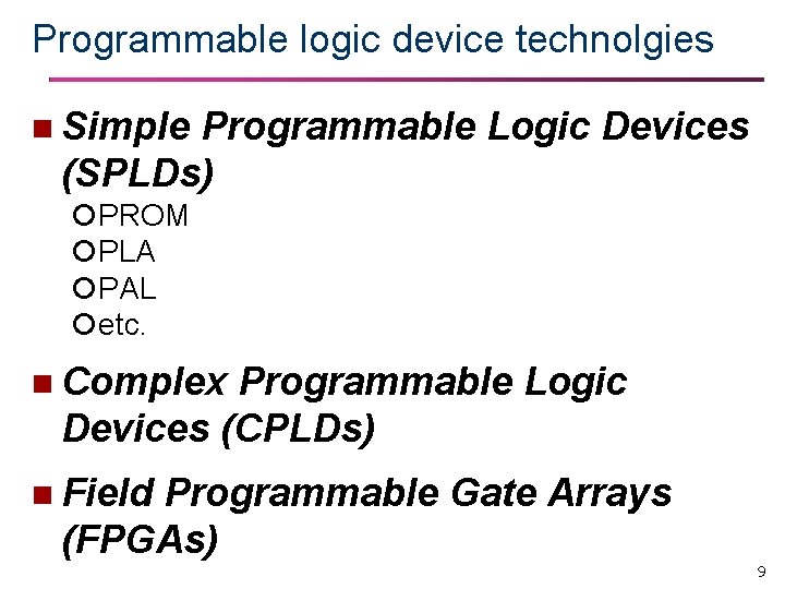
Programmable logic device technolgies n Simple Programmable Logic Devices (SPLDs) PROM PLA PAL etc. n Complex Programmable Logic Devices (CPLDs) n Field Programmable Gate Arrays (FPGAs) 9
![Simple programmable logic device 3 n Programmable logic array PLA allows Sum of Products Simple programmable logic device [3] n Programmable logic array (PLA) allows Sum of Products](https://slidetodoc.com/presentation_image_h2/229443b92688f5e4346ec41ee2ba6f08/image-10.jpg)
Simple programmable logic device [3] n Programmable logic array (PLA) allows Sum of Products (So. P) implementation [3] Clive Maxfield. (2004) The Design Warrior's Guide to FPGAs, Academic 10 Press, Inc. Orlando, FL, USA
![Complex programmable logic device 4 Cool RunnerII CPLD Family Data Sheet DS 090 v Complex programmable logic device [4] Cool. Runner-II CPLD Family Data Sheet, DS 090 (v](https://slidetodoc.com/presentation_image_h2/229443b92688f5e4346ec41ee2ba6f08/image-11.jpg)
Complex programmable logic device [4] Cool. Runner-II CPLD Family Data Sheet, DS 090 (v 3. 1). September 11, 11 2008

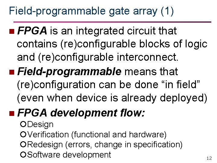
Field-programmable gate array (1) n FPGA is an integrated circuit that contains (re)configurable blocks of logic and (re)configurable interconnect. n Field-programmable means that (re)configuration can be done “in field” (even when device is already deployed) n FPGA development flow: Design Verification (functional and hardware) Redesign (errors, change in specification) Software development 12
![Conceptual structure of an FPGA 5 Chu P P 2008 References in FPGA Prototyping Conceptual structure of an FPGA [5] Chu, P. P. (2008) References, in FPGA Prototyping](https://slidetodoc.com/presentation_image_h2/229443b92688f5e4346ec41ee2ba6f08/image-13.jpg)
Conceptual structure of an FPGA [5] Chu, P. P. (2008) References, in FPGA Prototyping by VHDL Examples: Xilinx Spartan™-3 Version, John Wiley & Sons, Inc. , Hoboken, NJ, USA 13
![Threeinput LUTbased logic cell 5 Chu P P 2008 References in FPGA Prototyping by Three-input LUT-based logic cell [5] Chu, P. P. (2008) References, in FPGA Prototyping by](https://slidetodoc.com/presentation_image_h2/229443b92688f5e4346ec41ee2ba6f08/image-14.jpg)
Three-input LUT-based logic cell [5] Chu, P. P. (2008) References, in FPGA Prototyping by VHDL Examples: Xilinx Spartan™-3 Version, John Wiley & Sons, Inc. , Hoboken, NJ, USA 14
![Threeinput Look Up Table LUT 1 3 Clive Maxfield 2004 The Design Warriors Guide Three-input Look. Up Table (LUT) (1) [3] Clive Maxfield. (2004) The Design Warrior's Guide](https://slidetodoc.com/presentation_image_h2/229443b92688f5e4346ec41ee2ba6f08/image-15.jpg)
Three-input Look. Up Table (LUT) (1) [3] Clive Maxfield. (2004) The Design Warrior's Guide to FPGAs, Academic 15 Press, Inc. Orlando, FL, USA

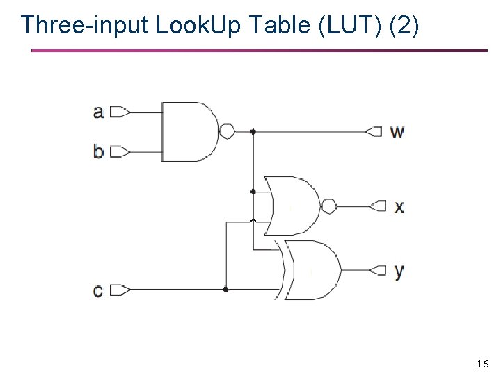
Three-input Look. Up Table (LUT) (2) 16

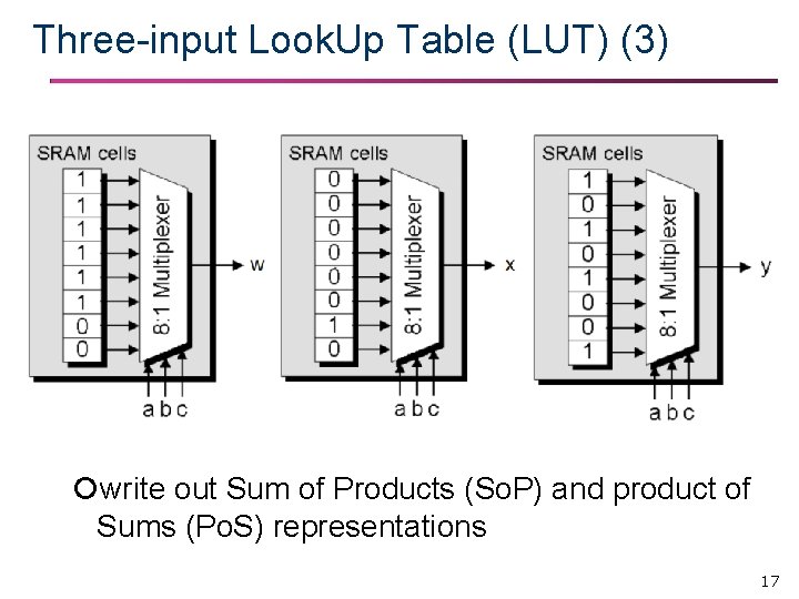
Three-input Look. Up Table (LUT) (3) write out Sum of Products (So. P) and product of Sums (Po. S) representations 17

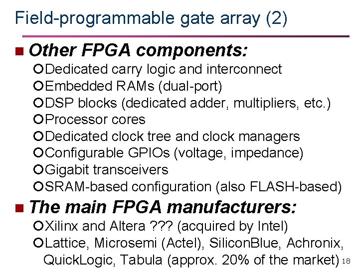
Field-programmable gate array (2) n Other FPGA components: Dedicated carry logic and interconnect Embedded RAMs (dual-port) DSP blocks (dedicated adder, multipliers, etc. ) Processor cores Dedicated clock tree and clock managers Configurable GPIOs (voltage, impedance) Gigabit transceivers SRAM-based configuration (also FLASH-based) n The main FPGA manufacturers: Xilinx and Altera ? ? ? (acquired by Intel) Lattice, Microsemi (Actel), Silicon. Blue, Achronix, Quick. Logic, Tabula (approx. 20% of the market) 18

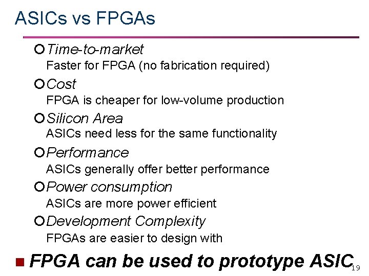
ASICs vs FPGAs Time-to-market Faster for FPGA (no fabrication required) Cost FPGA is cheaper for low-volume production Silicon Area ASICs need less for the same functionality Performance ASICs generally offer better performance Power consumption ASICs are more power efficient Development Complexity FPGAs are easier to design with n FPGA can be used to prototype ASIC 19

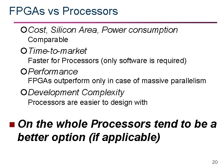
FPGAs vs Processors Cost, Silicon Area, Power consumption Comparable Time-to-market Faster for Processors (only software is required) Performance FPGAs outperform only in case of massive parallelism Development Complexity Processors are easier to design with n On the whole Processors tend to be a better option (if applicable) 20

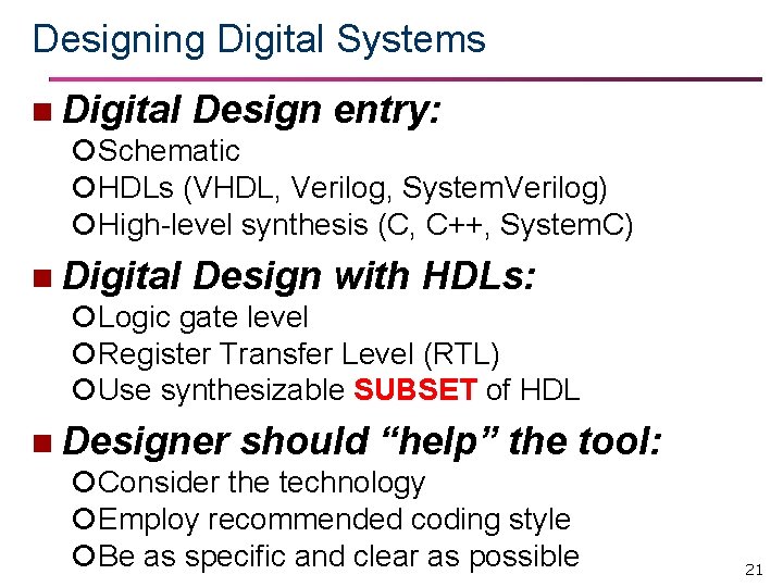
Designing Digital Systems n Digital Design entry: Schematic HDLs (VHDL, Verilog, System. Verilog) High-level synthesis (C, C++, System. C) n Digital Design with HDLs: Logic gate level Register Transfer Level (RTL) Use synthesizable SUBSET of HDL n Designer should “help” the tool: Consider the technology Employ recommended coding style Be as specific and clear as possible 21

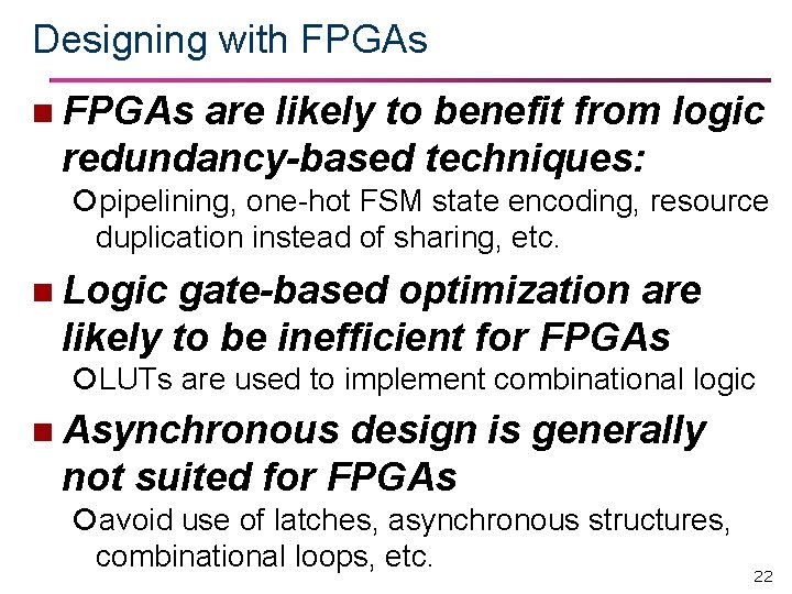
Designing with FPGAs n FPGAs are likely to benefit from logic redundancy-based techniques: pipelining, one-hot FSM state encoding, resource duplication instead of sharing, etc. n Logic gate-based optimization are likely to be inefficient for FPGAs LUTs are used to implement combinational logic n Asynchronous design is generally not suited for FPGAs avoid use of latches, asynchronous structures, combinational loops, etc. 22

IAY 0600 DIGITAL SYSTEMS DESIGN LABS Dmitri Mihhailov Tallinn University of Technology

Digital Systems Design Labs Staff n Lecturer: Alexander Sudnitson (associate professor) aleksander. sudnitson@ttu. ee ICT-503 (620 2255) n Lab Assistant: Dmitri Mihhailov (research scientist) dmitri. mihhailov@ttu. ee ICT-505 (no phone) n Technical Assistant: Artjem Rjabov (early stage research scientist) artjom. rjabov@ttu. ee ICT-512 (620 2265) 24

IAY 0600 Digital Systems Design Labs (1) n Lab Room: ICT-502 AB (~ 30 working places) ICT-405 (15 working places) Lab PCs require the same password that is used to access other computers in TUT network n Lab Time: GROUP A Wednesdays 16: 00 - 17: 30 (primary time) ICT-502 AB GROUP B Wednesdays 17: 45 - 19: 15 (reserve time) ICT-405 25

IAY 0600 Digital Systems Design Labs (2) n Lab Course webpage: http: //ati. ttu. ee/~alsu/ IAY 0600 l Digital Systems Design (WORKSHOPS) http: //ati. ttu. ee/~alsu/IAY 0600 l. html n The target lab course: LABS SET I (Xilinx FPGA-based) n The lab course consists of Tutorial (essentially not a lab) Set of compulsory labs (4 labs) Set of optional labs (5 labs) 10 labs: 26

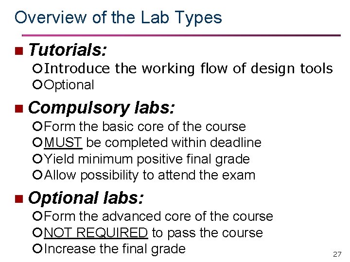
Overview of the Lab Types n Tutorials: Introduce the working flow of design tools Optional n Compulsory labs: Form the basic core of the course MUST be completed within deadline Yield minimum positive final grade Allow possibility to attend the exam n Optional labs: Form the advanced core of the course NOT REQUIRED to pass the course Increase the final grade 27

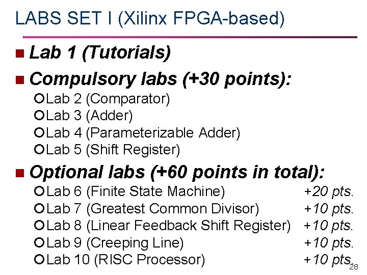
LABS SET I (Xilinx FPGA-based) n Lab 1 (Tutorials) n Compulsory labs (+30 points): Lab 2 (Comparator) Lab 3 (Adder) Lab 4 (Parameterizable Adder) Lab 5 (Shift Register) n Optional labs (+60 points in total): Lab 6 (Finite State Machine) +20 pts. Lab 7 (Greatest Common Divisor) +10 pts. Lab 8 (Linear Feedback Shift Register) +10 pts. Lab 9 (Creeping Line) +10 pts. Lab 10 (RISC Processor) +10 pts. 28

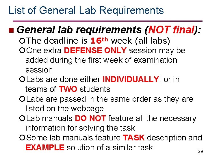
List of General Lab Requirements n General lab requirements (NOT final): The deadline is 16 th week (all labs) One extra DEFENSE ONLY session may be added during the first week of examination session Labs are done either INDIVIDUALLY, or in teams of TWO students Labs are passed in the same order as they are listed on the webpage Lab manuals DO NOT feature all the necessary information for solving the task Some lab manuals feature TASK description and EXAMPLE solution of a similar task 29

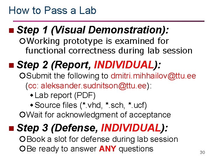
How to Pass a Lab n Step 1 (Visual Demonstration): Working prototype is examined for functional correctness during lab session n Step 2 (Report, INDIVIDUAL): Submit the following to dmitri. mihhailov@ttu. ee (cc: aleksander. sudnitson@ttu. ee): Lab report (PDF) Source files (*. vhd, *. sch, *. ucf) Wait for acknowledgment of acceptance n Step 3 (Defense, INDIVIDUAL): Book a slot for defense during lab session Be ready to answer ANY questions 30

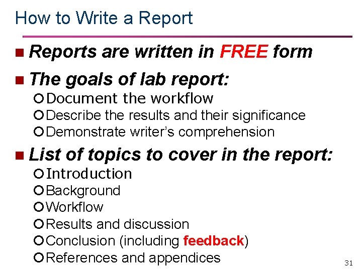
How to Write a Report n Reports are written in FREE form n The goals of lab report: Document the workflow Describe the results and their significance Demonstrate writer’s comprehension n List of topics to cover in the Introduction Background Workflow Results and discussion Conclusion (including feedback) References and appendices report: 31

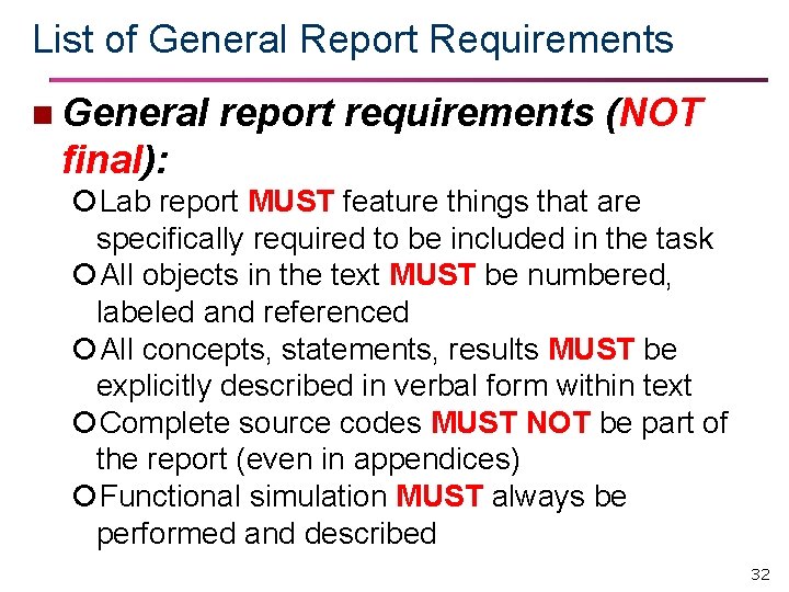
List of General Report Requirements n General report requirements (NOT final): Lab report MUST feature things that are specifically required to be included in the task All objects in the text MUST be numbered, labeled and referenced All concepts, statements, results MUST be explicitly described in verbal form within text Complete source codes MUST NOT be part of the report (even in appendices) Functional simulation MUST always be performed and described 32

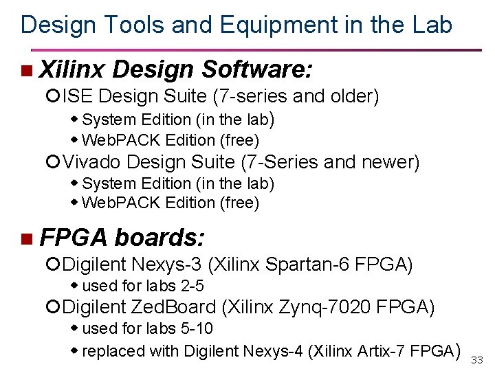
Design Tools and Equipment in the Lab n Xilinx Design Software: ISE Design Suite (7 -series and older) System Edition (in the lab) Web. PACK Edition (free) Vivado Design Suite (7 -Series and newer) System Edition (in the lab) Web. PACK Edition (free) n FPGA boards: Digilent Nexys-3 (Xilinx Spartan-6 FPGA) used for labs 2 -5 Digilent Zed. Board (Xilinx Zynq-7020 FPGA) used for labs 5 -10 replaced with Digilent Nexys-4 (Xilinx Artix-7 FPGA) 33

IAY 0600 DIGITAL SYSTEMS DESIGN XILINX ISE DESIGN SUITE OVERVIEW Dmitri Mihhailov Tallinn University of Technology

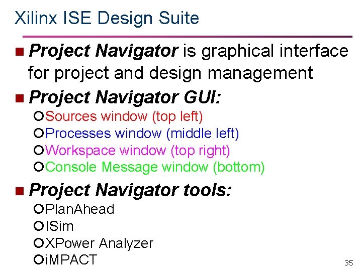
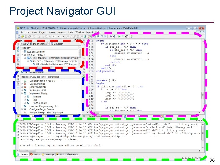
Xilinx ISE Design Suite n Project Navigator is graphical interface for project and design management n Project Navigator GUI: Sources window (top left) Processes window (middle left) Workspace window (top right) Console Message window (bottom) n Project Navigator Plan. Ahead ISim XPower Analyzer i. MPACT tools: 35

Project Navigator GUI 36

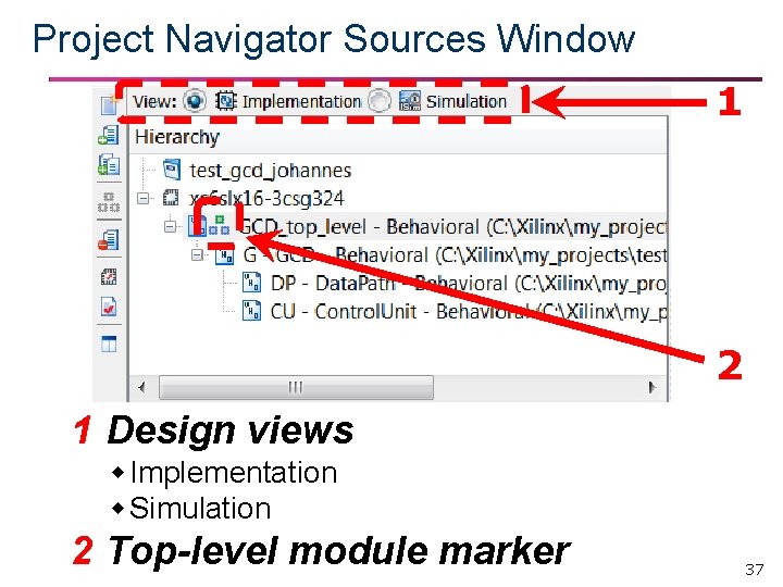
Project Navigator Sources Window 1 2 1 Design views Implementation Simulation 2 Top-level module marker 37

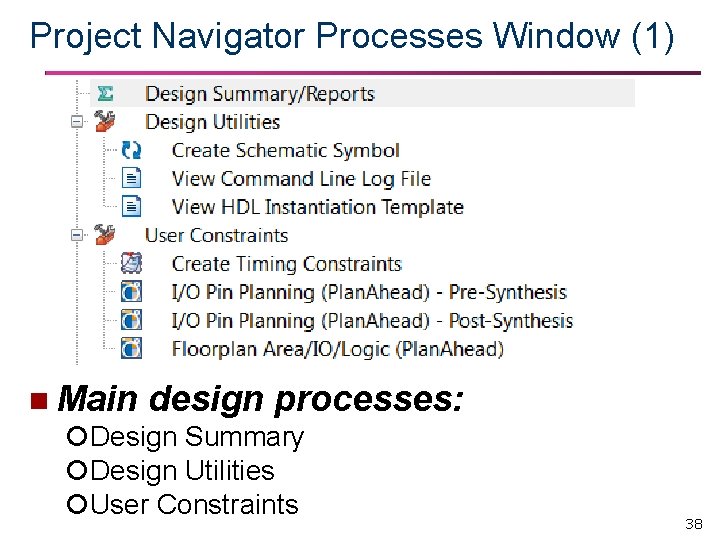
Project Navigator Processes Window (1) n Main design processes: Design Summary Design Utilities User Constraints 38

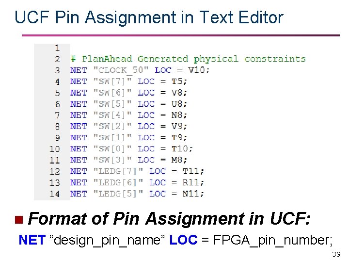
UCF Pin Assignment in Text Editor n Format of Pin Assignment in UCF: NET “design_pin_name” LOC = FPGA_pin_number; 39

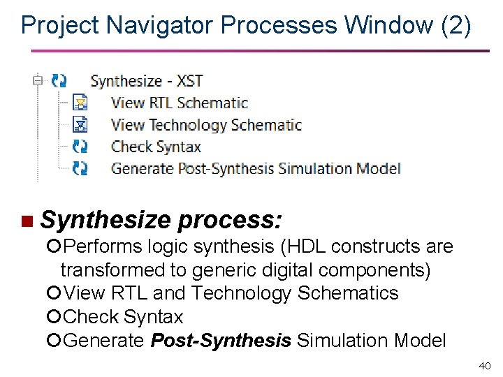
Project Navigator Processes Window (2) n Synthesize process: Performs logic synthesis (HDL constructs are transformed to generic digital components) View RTL and Technology Schematics Check Syntax Generate Post-Synthesis Simulation Model 40

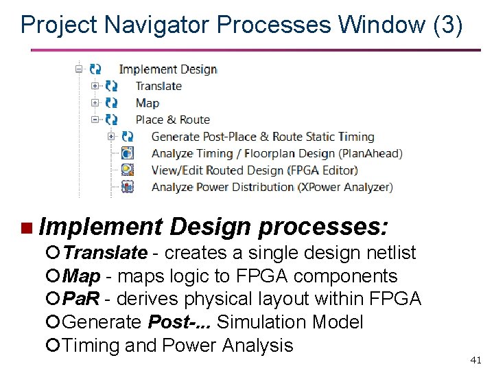
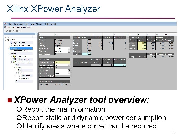
Project Navigator Processes Window (3) n Implement Design processes: Translate - creates a single design netlist Map - maps logic to FPGA components Pa. R - derives physical layout within FPGA Generate Post-. . . Simulation Model Timing and Power Analysis 41

Xilinx XPower Analyzer n XPower Analyzer tool overview: Report thermal information Report static and dynamic power consumption Identify areas where power can be reduced 42

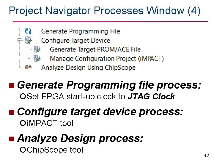
Project Navigator Processes Window (4) n Generate Programming file process: Set FPGA start-up clock to JTAG Clock n Configure target i. MPACT tool n Analyze Design Chip. Scope tool device process: 43

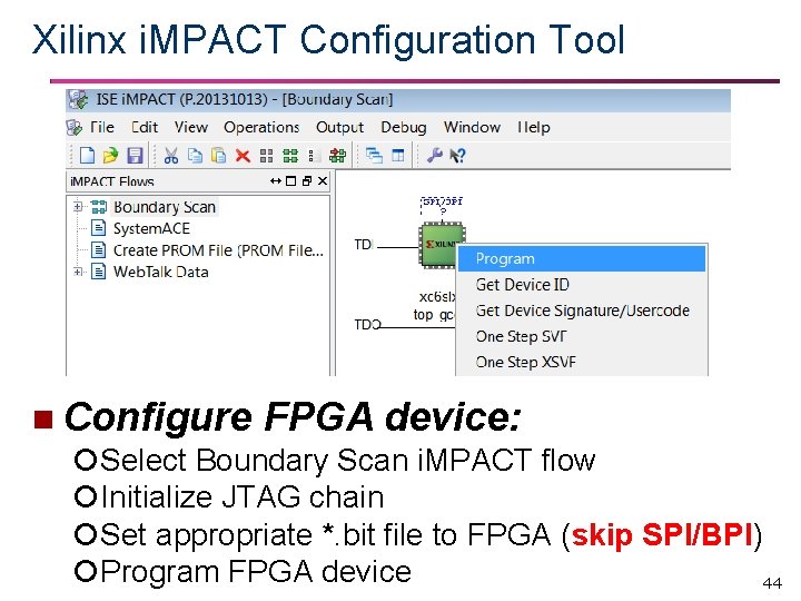
Xilinx i. MPACT Configuration Tool n Configure FPGA device: Select Boundary Scan i. MPACT flow Initialize JTAG chain Set appropriate *. bit file to FPGA (skip SPI/BPI) Program FPGA device 44

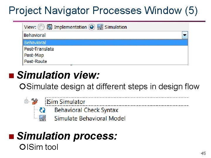
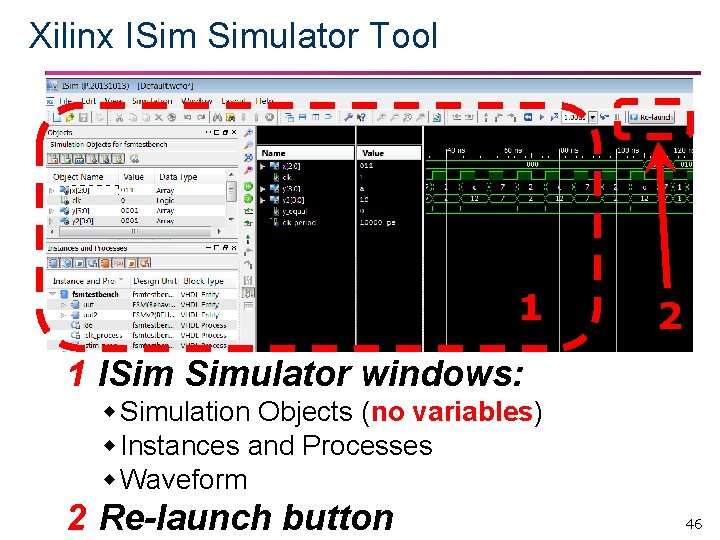
Project Navigator Processes Window (5) n Simulation view: Simulate design at different steps in design flow n Simulation ISim tool process: 45

Xilinx ISim Simulator Tool 1 2 1 ISim Simulator windows: Simulation Objects (no variables) Instances and Processes Waveform 2 Re-launch button 46

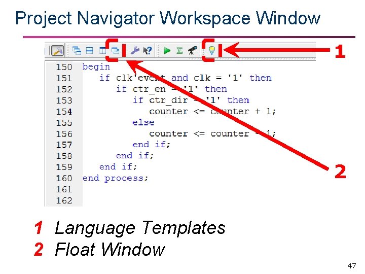
Project Navigator Workspace Window 1 2 1 Language Templates 2 Float Window 47

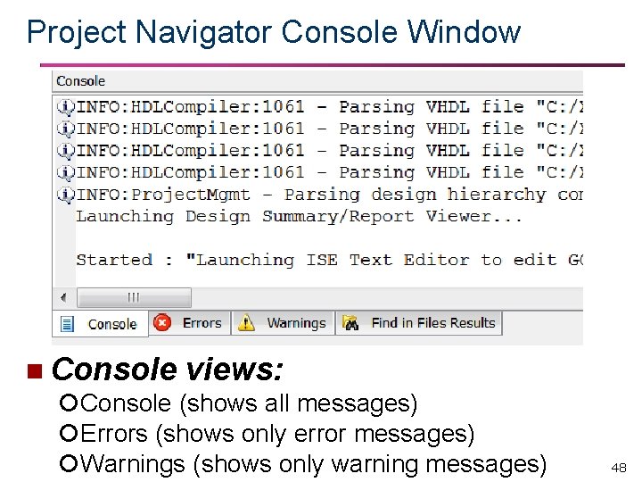
Project Navigator Console Window n Console views: Console (shows all messages) Errors (shows only error messages) Warnings (shows only warning messages) 48
![Nexys3 FPGA Board 1 6 n Nexys3 FPGA board features Xilinx Spartan6 XC 6 Nexys-3 FPGA Board (1) [6] n Nexys-3 FPGA board features: Xilinx Spartan-6 XC 6](https://slidetodoc.com/presentation_image_h2/229443b92688f5e4346ec41ee2ba6f08/image-49.jpg)
Nexys-3 FPGA Board (1) [6] n Nexys-3 FPGA board features: Xilinx Spartan-6 XC 6 LX 16 -CS 324 -3 Total of 48 Mbytes of external memory 10/100 Ethernet port micro USB port for power and programming micro USB UART port Type-A USB host port VGA port Four Pmod and one VHDC GPIO connectors Eight slide switches, five push buttons and eight LEDs, four-digit seven-segment display 100 MHz fixed-frequency oscillator [6] Nexys 3 FPGA Board Reference Manual, Digilent Inc. , April 11, 2016. 49
![Nexys3 FPGA Board 2 6 Nexys 3 FPGA Board Reference Manual Digilent Inc Nexys-3 FPGA Board (2) [6] Nexys 3 FPGA Board Reference Manual, Digilent Inc. ,](https://slidetodoc.com/presentation_image_h2/229443b92688f5e4346ec41ee2ba6f08/image-50.jpg)
Nexys-3 FPGA Board (2) [6] Nexys 3 FPGA Board Reference Manual, Digilent Inc. , April 11, 2016. 50